

Page 1
SECTION 4
CHARTS AND DIAGRAMS
NOTES OF SCHEMATIC DIAGRAM
Safety precautions
The Components identified by the symbol are
critical for safety. For continued safety, replace safety
critical components only with manufacturer's recommended parts.
1. Units of components on the schematic diagram
Unless otherwise specified.
1) All resistance values are in ohm. 1/6 W, 1/8 W (refer to
parts list).
Chip resistors are 1/16 W.
K: KØ (1000Ø), M: MØ (1000KØ)
2) All capacitance values are in µF, (P: PF).
3) All inductance values are in µH, (m: mH).
4) All diodes are 1SS133, MA165 or 1N4148M (refer to parts
list).
4. Voltage measurement
1) Regulator (DC/DC CONV) circuits
REC : Colour bar signal.
PB : Alignment tape (Colour bar).
— : Unmeasurable or unnecessary to measure.
4) Indication on schematic diagram
Voltage Indications for REC and PB mode on the schematic diagram are as shown below.
REC mode
12 3
2.5
(5.0)
PB mode
1.8
PB and REC modes
(Voltage of PB and REC modes
are the same)
Note: If the voltages are not indicated on the schematic
diagram, refer to the voltage charts.
CIRCUIT BOARD NOTES
1. Foil and Component sides
1) Foil side (B side) :
Parts on the foil side seen from foil face (pattern face)
are indicated.
2) Component side (A side) :
Parts on the component side seen from component face
(parts face) indicated.
2. Parts location guides
Parts location are indicated by guide scale on the circuit board.
LOCATION
IC
Category : IC
Horizontal “A” zone
Vertical “6” zone
(A : Component side)
D : Discrete component)
B : Foil side
C : Chip component
REF No.
IC101 B C 6 A
2. Indications of control voltage
AUX : Active at high.
AUX or AUX(L) : Active at low.
3. Interpreting Connector indications
1
2
Removable connector
3
1
2
Wire soldered directly on board
3
1
Non-removable Board connector
2
3
1
2
4
Board to Board
3
5. Signal path Symbols
The arrows indicate the signal path as follows.
NOTE : The arrow is DVC unique object.
Playback signal path
Playback and recording signal path
Recording signal path
(including E-E signal path)
Capstan servo path
Drum servo path
(Example)
R-Y
Playback R-Y signal path
Y
Recording Y signal path
6. Indication of the parts for adjustments
The parts for the adjustments are surrounded with the circle as
shown below.
Note: For general information in service manual, please
refer to the Service Manual of GENERAL INFORMATION Edition 4 No. 82054D (January 1994).
S40889-01
Connected pattern on board
The arrows indicate signal path
7. Indication of the parts not mounted on the circuit board
“OPEN” is indicated by the parts not mounted on the circuit
board.
R216
OPEN
4-1
4-2
S40889-01
Page 2
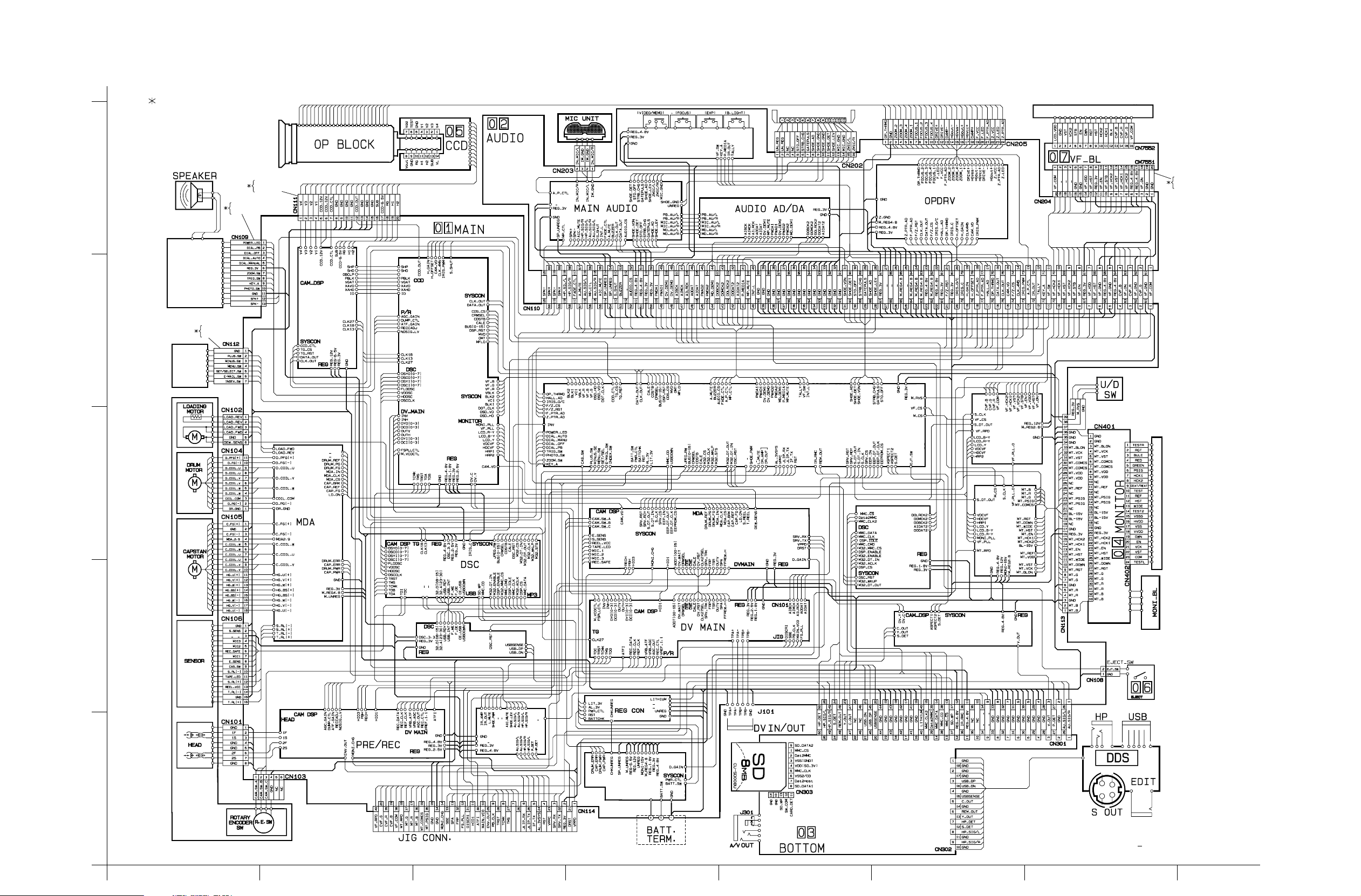
4.1 BOARD INTERCONNECTIONS
NOTE): The number of patch cords
are indicated by interconnected.
5
OPE. COVER
UNIT
(
)
Page 4-49
4
YTU94074-7
YTU94077-7
SUB
OPE.
UNIT
(
)
Page 4-49
3
YTU94074-13
YTU94077-13
YTU94074-20
YTU94077-20
TG/VDR
(
Page 4-19
(
Page 4-9
LCD MODULE
WBSE/TALLY
(
)
P/R
REG 12V/NC
REG
,
REG CON
Page 4-37
AUDIO AD/DA
CAM. DSP
CN114
MAIN AUDIO
CN110
SYSCON-CPU
(
)
Page 4-5
MSD-CPU
XI164SEL
(
Page 4-39
CN201
REG CON
(
Page 4-7
HP DET
CN110
P DET
CN102
)
DAMP
DAMP
(
)
)
CN201
GND/Z GND
GND/Z GND
CN110
W/B
CN114
CN107
CN114
MSD
CN110
CN110
CN107
AUDIO MP3
(
Page 4-31
Page 4-43
GND/Z GND
GND/Z GND
VF MAIN
(
)
Page 4-27
CN108
CN110
MONITOR MAIN
(
)
Page 4-27
)
CVF B
CVF R
CVF G
)
Page 4-47
(
YTU94074-20
YTU94077-20
MODULE
)
MONITOR
(
LCD
(
)
Page 4-36
CN201
CN203
M REG4.8
(
)
Page 4-41
CN201
TG/VDR
OBCLP
CN201
)
CAM. DSP
(
)
Page 4-17
CN110
TG/VDR
MSD
T REEL
S REEL
CN114
)
CN114
CN107
MMC CD
MMC DATA
(
Page 4-29
MSD
VIDEO
OUT
)
CN106
CN103
CN106
XI164SEL
(
2
1
PTR3
MSD
(
Page 4-13
USBDRV
(
)
Page 4-33
REGCON,W/B
REG 12V
SYSCON
P DET
BOTTOM
HP DET
CN110
(
Page 4-23,35
CN11
REG 3V
)
CN114
SYSCON
(
Page 4-23
)
SP UNREG
M REG4.8
)
MSD
)
TDC
,
TDA
,
TDO/TDO
TDB
,
TDI/TDI
MSD
REG
(
Page 4-25
Page 4-11
)
J101
CN107
(
Page 4-45
)
4-3 4-4
VIDEO OUT
(
)
Page 4-15
SD 3V/REG 3V
SD 3V/REG 3V
y10210001a rev0
HGFEDCBA
Page 3
4.2 SYSCON-CPU SCHEMATIC DIAGRAM
For the destination of each signal and further line connections that are cut off fromNOTES :
this diagram,refer to "4.1 BOARD INTERCONNECTIONS".
When ordering parts,be sure to order according to the Part Number indicated in the Parts List.
5
4
TO REG CON
TO REG
TO REG CON
TO R EG
TO R EG C ON
TO W /B
TO
REG CON
TO
EJECT SW
TO CAM. DSP
,
TG/VDR
REG CON
TO CAM. DSP
TO REG
,
CN108
MAIN(SYSCON-CPU
)
TO MSD-CPU
TO MSD-CPU
VF MAIN
MONITOR MAIN
TO MSD-CPU
TO
MSD-CPU
TO DSC
TO DSC
AUDIO MP3
TO DSC
TO USBDRV
TO REG CON
TO DSC,AUDIO MP3
TO DSC
TO CAM. DSP,DSC
TO DSC
,
,
,
3
2
1
TO TG/VDR
TO CAM. DSP
TO TG/VDR
TO REG CON
TO
REG CON
TO
REG CON
TO R EG
TO
OPE. COVER UNIT
TO
SUB OPE. UNIT
TO VF MAIN
CN109
CN112
UPD70F3040F1-A13
UPD703039F1-A13
TO REG CON
TO VIDEO OUT
TO VIDEO OUT
TO REG CON
TO CAM. DSP
TO
REG CON
TO
CAM. DSP
TO REG CON
TO MSD-CPU
TO
REG CON
NO WEAR
ABCD EFGH
4-5 4-6
y10213001a rev0
Page 4
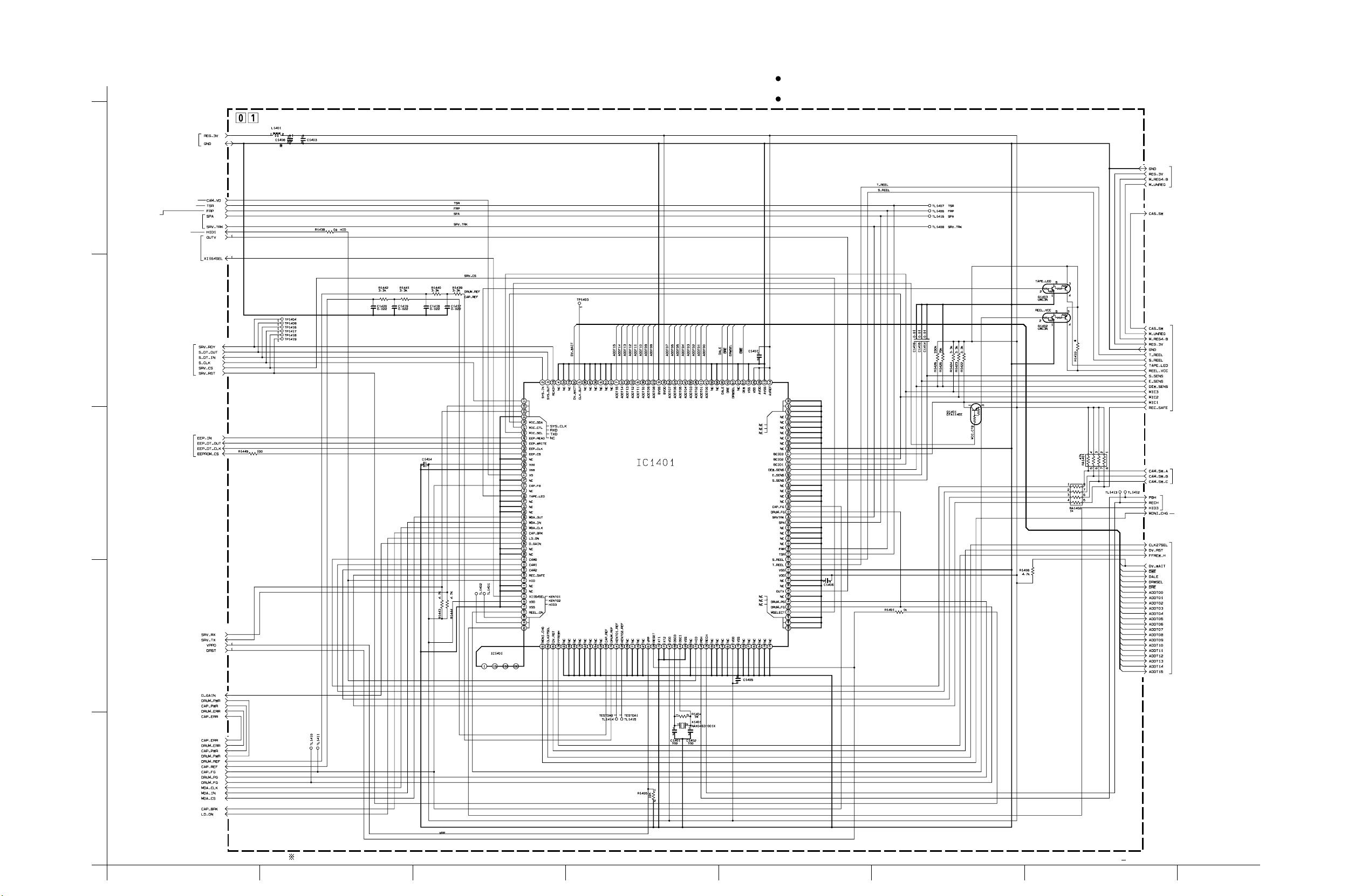
4.3 MSD-CPU SCHEMATIC DIAGRAM
For the destination of each signal and further line connections that are cut off fromNOTES :
this diagram,refer to "4.1 BOARD INTERCONNECTIONS".
When ordering parts,be sure to order according to the Part Number indicated in the Parts List.
5
4
TO CAM. DSP
TO DV MAIN
,
TO DV MAIN
REG CON
TO DV MAIN,PRE/REC
REC CON
TO DV MAIN
TO DV MAIN
TO SYSCON
TO REG
,
MAIN(MSD-CPU
NQR0006-001X
0.1
)
TO REG
TO SYSCON-CPU
0.1
TO MDA
TO SYSCON
0.1
3
UPD70F3040YFM01
UPD703040YF-M01
0.1
TO REC CON
TO MDA
TO PRE/REC
TO REG CON
TO DV MAIN
2
TO REG
TO MDA
0.1
1
NO WEAR
4-7 4-8
y10214001a rev0
HGFEDCBA
Page 5
5
4
4.4 MDA SCHEMATIC DIAGRAM
TO
MSD-CPU
TO REG
MAIN(MDA
For the destination of each signal and further line connections that are cut off fromNOTES :
this diagram,refer to "4.1 BOARD INTERCONNECTIONS".
When ordering parts,be sure to order according to the Part Number indicated in the Parts List.
)
TO
CAPSTAN MOTOR
CN105
3
VCC
TO REG
TO SENSOR
CN106
IC1702
TA75W393FU
VEE
2
TO
DRUM MOTOR
CN104
VCC
VEE
IC1701
TA75W01FU
TO
ROTARY ENCODER SW
CN103
TO
LOADING MOTOR
1
NO WEAR
ABCD EFGH
4-9 4-10
y20135001a rev0
CN102
Page 6
4.5 DV MAIN SCHEMATIC DIAGRAM
For the destination of each signal and further line connections that are cut off fromNOTES :
this diagram,refer to "4.1 BOARD INTERCONNECTIONS".
When ordering parts,be sure to order according to the Part Number indicated in the Parts List.
5
4
TO
REG CON
TO CAM. DSP
TO REG
(
DV MAIN
)
TO
CAM. DSP
,
TO MSD-CPU
CAM. DSP
TO CAM. DSP
TO TG/VDR
TO REG CON
TO
MSD-CPU
3
TO MSD-CPU
TO MSD-CPU
TO MSD-CPU,REG CON
TO MSD-CPU
2
TO
PRE/REC
1
TO JIG CONN
TO CAM. DSP
NO WEAR
4-11 4-12
y10215001a rev0
HGFEDCBA
Page 7
4.6 PRE/REC SCHEMATIC DIAGRAM
For the destination of each signal and further line connections that are cut off fromNOTES :
this diagram,refer to "4.1 BOARD INTERCONNECTIONS".
When ordering parts,be sure to order according to the Part Number indicated in the Parts List.
5
TO MSD-CPU
TO REG CON
4
TO
CAM. DSP
TO HEAD
3
TO
DV MAIN
2
TO REG CON
ATFI
1
TO REG
TO CAM. DSP
TO REG
NO WEAR
ABCD EFGH
4-13 4-14
y20136001a rev0
Page 8
4.7 VIDEO OUT SCHEMATIC DIAGRAM
For the destination of each signal and further line connections that are cut off fromNOTES :
this diagram,refer to "4.1 BOARD INTERCONNECTIONS".
When ordering parts,be sure to order according to the Part Number indicated in the Parts List.
5
TO REG
4
TO REG CON
TO REG CON
3
TO CAM. DSP
2
1
TO
SYSCON-CPU
NO WEAR
y30143001a rev0
4-15 4-16
HGFEDCBA
Page 9

4.8 CAM. DSP SCHEMATIC DIAGRAM
For the destination of each signal and further line connections that are cut off fromNOTES :
this diagram,refer to "4.1 BOARD INTERCONNECTIONS".
When ordering parts,be sure to order according to the Part Number indicated in the Parts List.
TO VF MAIN
TO MONITOR MAIN
TO VF MAIN
MONITOR MAIN
TO DV MAIN
TO SYSCON-CPU
DV MAIN
TO DV MAIN
TO REG CON
,
,
TO
TG/VDR
MAIN
(
CAM. DSP
)
5
TO CCD
4
TO PRE/REC
TO
DV MAIN
TO
MONITOR MAIN
3
TO SYSCON-CPU
TO SYSCON
TO REG CON
TO VIDEO OUT
TO
VF MAIN
MONITOR MAIN
TO DV MAIN
PRE/REC
,
,
2
,
TO MSD-CPU
REG CON
TO REG CON
TO
REG CON
1
TO DSC
TO REG
NO WEAR
ABCD EFGH
: Difference point
4-17 4-18
y10216001a rev0
Page 10
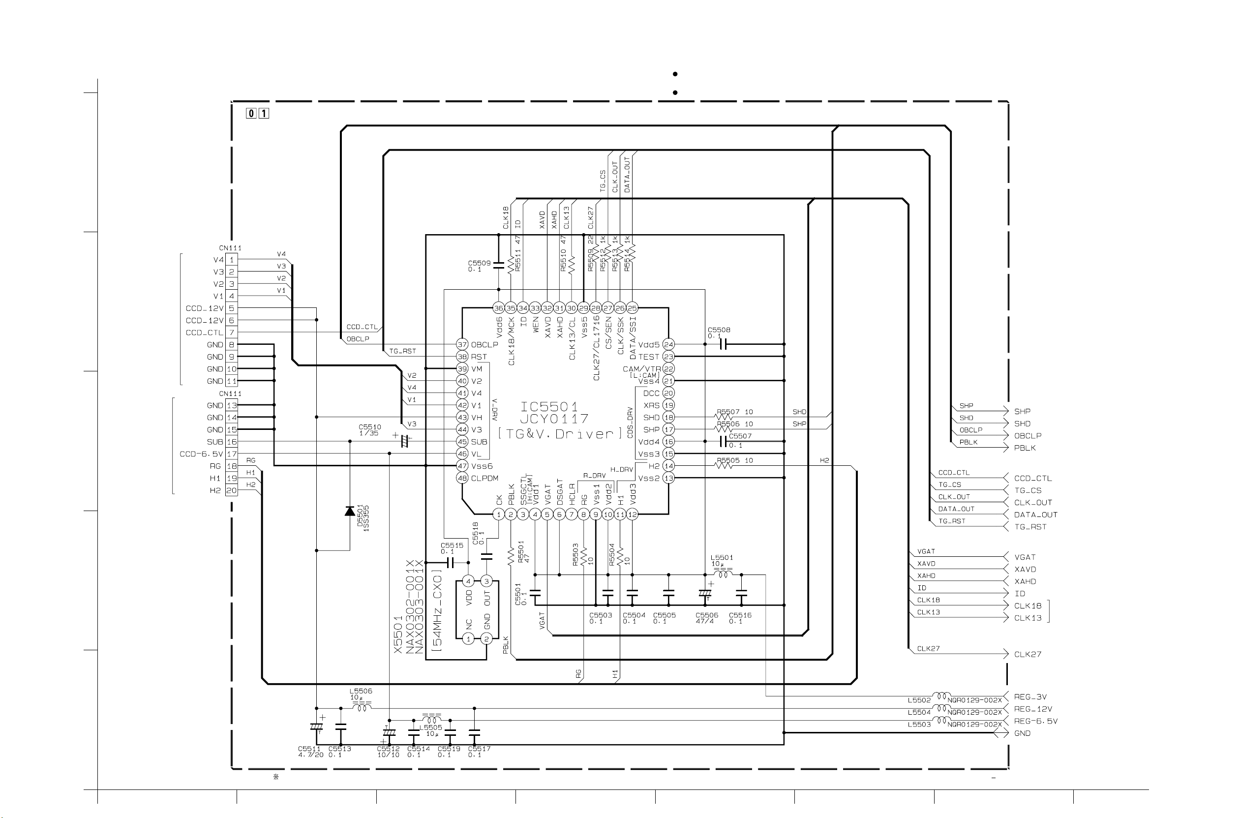
4.9 TG/VDR SCHEMATIC DIAGRAM
For the destination of each signal and further line connections that are cut off fromNOTES :
this diagram,refer to "4.1 BOARD INTERCONNECTIONS".
When ordering parts,be sure to order according to the Part Number indicated in the Parts List.
MAIN(TG/VDR
)
5
4
TO CCD
CN5001
TO CAM. DSP
3
TO CCD
CN5001
TO SYSCON CPU
2
TO CAM. DSP
DSC
TO CAM. DSP
DV MAIN
TO REG
,
,
1
NO WEAR
4-19 4-20
y30144001a rev0
HGFEDCBA
Page 11
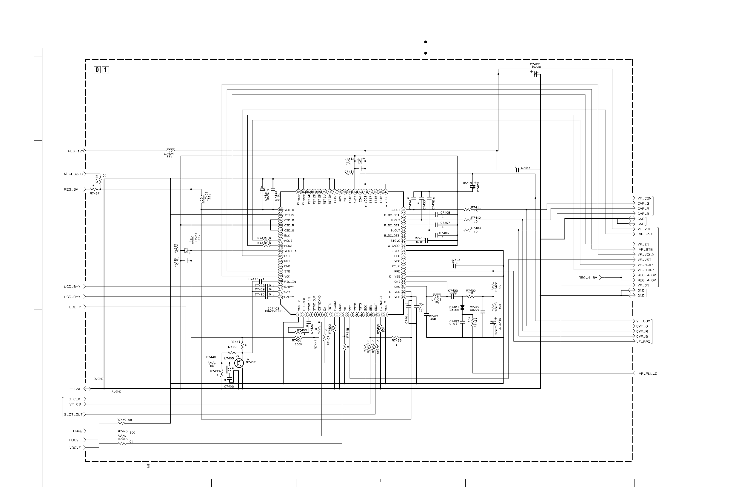
4.10 VF MAIN SCHEMATIC DIAGRAM
For the destination of each signal and further line connections that are cut off fromNOTES :
this diagram,refer to "4.1 BOARD INTERCONNECTIONS".
When ordering parts,be sure to order according to the Part Number indicated in the Parts List.
5
4
TO REG
TO
MONITOR MAIN
(
)
OPEN
MAIN(VF MAIN
)
TO REG CON
TO REG
3
2
TO
SYSCON-CPU
TO
CAM. DSP
TO REG
TO CAM. DSP
TO REG
TO REG
TO REG CON
TO
MONITOR MAIN
TO REG CON
1
NO WEAR
ABCD EFGH
4-21 4-22
y10218001a rev0
Page 12

4.11 REG CON SCHEMATIC DIAGRAM
For the destination of each signal and further line connections that are cut off fromNOTES :
this diagram,refer to "4.1 BOARD INTERCONNECTIONS".
When ordering parts,be sure to order according to the Part Number indicated in the Parts List.
TO AUDIO
CN201
5
TO REG
TO SYSCON-CPU
TO VF MAIN
VF MAIN
TO
VF MAIN
TO
TO W/B
TO SYSCON-CPU
TO CAM. DSP
TO SYSCON-CPU
TO SYSCON-CPU
TO CAM. DSP
TO SYSCON-CPU
TO CAM. DSP
TO DSC
TO SYSCON-CPU
TO SYSCON-CPU
SYSCON-CPU
TO
AUDIO MP3
TO
TO
TO
SYSCON-CPU
DV MAIN
SYSCON-CPU
TO
TO REG
TO CAM. DSP
TO SYSCON-CPU
TO SYSCON-CPU
TO REG
TO D2703
TO R2701
TO R2702
TO SYSCON-CPU
TO SYSCON-CPU
TO R2707
TO R2706
TO SYSCON-CPU
4
3
2
TO REG
TO
MONITOR MAIN
TO MSD-CPU
PRE/REC
TO DV MAIN
TO MSD-CPU
TO DV MAIN
TO MSD-CPU
TO PRE/REC
TO DV MAIN
TO PRE/REC
TO DV MAIN
TO DV MAIN
DSC,CAM. DSP
TO
VF MAIN
,
TO SYSCON-CPU
MAIN(REG CON
,
)
TO VIDEO OUT
TO REG
TO REG
TO SYSCON-CPU
REG
TO CN110
SYSCON-CPU
TO
TO
AUDIO MP3
TO REG CON
DSC
,
,
TO SYSCON-CPU
TO DSC
TO
DSC
TO AUDIO MP3
NC
NC
TO BOTTOM
CN301
TO USBDRV
TO REG
TO
SYSCON-CPU
TO
MSD-CPU
TO
MSD-CPU
TO SYSCON-CPU
TO SYSCON-CPU
1
NO WEAR
TO VIDEO OUT
TO VIDEO OUT
TO SYSCON-CPU
y20146001a rev0
4-23 4-24
NC
NC
HGFEDCBA
Page 13

4.12 REG SCHEMATIC DIAGRAM
For the destination of each signal and further line connections that are cut off fromNOTES :
this diagram,refer to "4.1 BOARD INTERCONNECTIONS".
When ordering parts,be sure to order according to the Part Number indicated in the Parts List.
TO SYSCON-CPU
TO
REG CON
TO MDA
TO SYSCON CPU,W/B
MSD-CPU,MDA
DV MAIN,PRE/REC
5
VIDEO OUT,CAM. DSP
TG/VDR,REG CON
VF MAIN,MONITOR MAIN
DSC,USBDRV,AUDIO MP3
,
TO REG CON
,
,
,
,
,
,
,
,
,
,
BATT.
TERM
TO SYSCON-CPU
MSD-CPU,MDA
DV MAIN,PRE/REC
CAM. DSP,TG/VDR
REG CON,DSC
AUDIO MP3
TO DVMAIN
CAM. DSP
AUDIO MP3
4
TO MSD-CPU
TO MSD-CPU
3
TO W/B,PRE/REC
VIDEO OUT,CAM. DSP
REG CON,MONITOR MAIN
DSC
,
,
,
TO MSD-CPU
MDA,REG CON
,
TO MONITOR MAIN
TO TG/VDR
2SA1577/RS/-X
2
2SC4617/QR/-X
MA8043/L/-X
,
TO TG/VDR
,
REG CON
,
VF MAIN
MONITOR MAIN
TO MSD-CPU
1
NO WEAR
y20137001a rev0
ABCD EFGH
4-25 4-26
Page 14

4.13 MONITOR MAIN SCHEMATIC DIAGRAM
For the destination of each signal and further line connections that are cut off fromNOTES :
this diagram,refer to "4.1 BOARD INTERCONNECTIONS".
When ordering parts,be sure to order according to the Part Number indicated in the Parts List.
TO
REG CON
MAIN(MONITOR MAIN
5
)
(
CN113-19,20
)
MT PSIG
CN113
[22,23]
TO
MONITOR MAIN
TO REG
TO REG
TO
LCD MODULE
CN402
4
3
TO REG
TO
VF MAIN
TO REG
TO
CAM. DSP
CN113
[14]
[15]
[12]
[13]
[32]
[31]
[9]
VIN VIN
CON
GND
IC7802
MM1385HN
NOISE
[27,28]
TO REG CON
MT COMCS
[7,8]
[4,5]
[1,2]
TO REG CON
CN113
[29,30]
TO REG CON
TO VF MAIN
TO CAM. DSP
TO
MONITOR MAIN
TO REG
TO
MONITOR MAIN
TO
MONITOR MAIN
TO REG
TO REG
2
1
TO
CAM. DSP
TO REG
TO
SYSCON-CPU
TO
CAM. DSP
NO WEAR
4-27 4-28
0.0012
y10219001a rev0
TO CAM. DSP
CN113
[25]
[33]
[11]
[10]
HGFEDCBA
Page 15

4.14 DSC SCHEMATIC DIAGRAM
For the destination of each signal and further line connections that are cut off fromNOTES :
this diagram,refer to "4.1 BOARD INTERCONNECTIONS".
When ordering parts,be sure to order according to the Part Number indicated in the Parts List.
MAIN(DSC
5
TO REG
(
)
OPEN
TO REG
TO USBDRV
TO REG
)
TO
USBDRV
TO
AUDIO MP3
TO REG CON
,
TO REG CON
AUDIO MP3
TO
USBDRV
4
TO CAM. DSP
TO
USBDRV
TO
SYSCON-CPU
3
2
1
TO AUDIO MP3
TO SYSCON-CPU
TO SYSCON-CPU
AUDIO MP3
TO SYSCON-CPU
TO TG/VDRV
TO REG CON
TO CAM. DSP
TO TG/VDRV
TO USBDRV
TO SYSCON-CPU
,
SN74AHC1G00K
TO REG CON
TO REG CON
TO USBDRV
TO
AUDIO MP3
NO WEAR
ABCD EFGH
: Difference point
4-29 4-30
y10217001a rev0
Page 16

4.15 AUDIO MP3 SCHEMATIC DIAGRAM
For the destination of each signal and further line connections that are cut off fromNOTES :
this diagram,refer to "4.1 BOARD INTERCONNECTIONS".
When ordering parts,be sure to order according to the Part Number indicated in the Parts List.
MAIN
5
TO REG CON
4
TO
REG CON
(
AUDIO MP3
)
3
TO
SYSCON-CPU
DSC
2
TO
SYSCON-CPU
1
TO DSC
TO DSC
TO DSC
TO DSC
,
TO
SYSCON-CPU
TO REG
NO WEAR
4-31 4-32
y20133001a rev0
HGFEDCBA
Page 17

4.16 USBDRV SCHEMATIC DIAGRAM
For the destination of each signal and further line connections that are cut off fromNOTES :
this diagram,refer to "4.1 BOARD INTERCONNECTIONS".
When ordering parts,be sure to order according to the Part Number indicated in the Parts List.
MAIN(USBDRV
)
5
TO DSC
4
TO REG
3
TO DSC
TO REG CON
TO DSC
TO REG
TO DSC
TO SYSCON-CPU
2
TO DSC
TO DSC
VSS
1
TO SYSCON-CPU
DSC
ABCD EFGH
,
NO WEAR
4-33 4-34
OUTNCVDD
TO REG CON
RB751V-40-X
y30146001a rev0
Page 18

4.17 W/B SCHEMATIC DIAGRAM 4.18 CCD SCHEMATIC DIAGRAM
For the destination of each signal and further line connections that are cut off fromNOTES :
this diagram,refer to "4.1 BOARD INTERCONNECTIONS".
When ordering parts,be sure to order according to the Part Number indicated in the Parts List.
IC5001 is incorporated in the CCD base assembly.
When IC5001 needs replacement,replace the CCD
5
For the destination of each signal and further line connections that are cut off fromNOTES :
this diagram,refer to "4.1 BOARD INTERCONNECTIONS".
When ordering parts,be sure to order according to the Part Number indicated in the Parts List.
5
base assembly in whole because it cannot be replaced alone.
CCD
MAIN(W/B
)
TO REG
4
TO
SYSCON-CPU
REG CON
TO
SYSCON-CPU
3
y40078001a rev0
2
4
,
TO
TG/VDR
CN111
TO CAM. DSP
CN111
3
TO
TG/VDR
CN111
2
1 1
DCBA
4-35 4-36
NO WEAR
: Difference point
y40077001a rev0
ABCD
Page 19

4.19 WBSE/SW SCHEMATIC DIAGRAM
TO VF MAIN
CN110
this diagram,refer to "4.1 BOARD INTERCONNECTIONS".
When ordering parts,be sure to order according to the Part Number indicated in the Parts List.
5
For the destination of each signal and further line connections that are cut off fromNOTES :
REG 3V
,
TO CN204
TO CN204
TO CN204
VF SW
4
TO R9902
TO C1152
TO OPDRV
TO MAIN AUDIO
TO
MAIN AUDIO
MAIN AUDIO
TO
OPDRV
TALLY LAMP
TO OPDRV
TO OPDRV
TO OPDRV
,
TO L1151
OPDRV
TO OPDRV
,
TO OPDRV
TO OPDRV
AUDIO AD/DA
TO MAIN AUDIO
TO MAIN AUDIO
TO AUDIO AD/DA
TO AUDIO AD/DA
P MEDIA
BACK LIGHT
/VOL.
EXPOSURE
/VOL.
TO CN201
FOCUS
/BLANK
TO MAIN AUDIO
VIDEO
MEMORY
TO CN201
3
W/B SENS
TO CN201
REG 3V
2
AUDIO
(
WBSE/SW
)
TO CN201
TO
VF BL
CN7551
y10212001a reV0
1
ABCD EFGH
4-37 4-38
Page 20

4.20 AUDIO AD/DA SCHEMATIC DIAGRAM
For the destination of each signal and further line connections that are cut off fromNOTES :
this diagram,refer to "4.1 BOARD INTERCONNECTIONS".
When ordering parts,be sure to order according to the Part Number indicated in the Parts List.
5
4
TO
MAIN AUDIO
AUDIO(AUDIO AD/DA
)
TO WBSE/SW
TO REG CON
TO WBSE/SW
3
2
TO WBSE/SW
1
NO WEAR
4-39 4-40
y30142001a rev0
HGFEDCBA
Page 21

4.21 MAIN AUDIO SCHEMATIC DIAGRAM
For the destination of each signal and further line connections that are cut off fromNOTES :
this diagram,refer to "4.1 BOARD INTERCONNECTIONS".
When ordering parts,be sure to order according to the Part Number indicated in the Parts List.
UN REG
UN REG
NC
NC
STO OFF
STRB CHG
TO
5
SHOE MIC
GATEPULS
SHOE AD
SHOE GND
SHOE GND
SHOE DET
SHOE LEV
MIC GND
MIC GND
TO WBSE/SW
ZMIC/L
ZMIC/R
TO
WBSE/SW
4
TO
MIC UNIT
LA74206W
TO WBSE/SW
TO
AUDIO AD/DA
TO WBSE/SW
TO WBSE/SW
3
TO WBSE/SW
TO WBSE/SW
TO WBSE/SW
2
TO WBSE/SW
TO WBSE/SW
1
AUDIO(MAIN AUDIO
NO WEAR
ABCD EFGH
)
y10211001a rev0
4-41 4-42
Page 22

4.22
OPDRV SCHEMAITC DIAGRAM
For the destination of each signal and further line connections that are cut off fromNOTES :
this diagram,refer to "4.1 BOARD INTERCONNECTIONS".
When ordering parts,be sure to order according to the Part Number indicated in the Parts List.
AUDIO(OPDRV
)
5
4
TO WBSE/SW
TO WBSE/SW
TO
OP BLOCK
CN205
3
TO WBSE/SW
TO WBSE/SW
2
Vdd
1
NO WEAR
4-43 4-44
y20145001a rev0
HGFEDCBA
Page 23

4.23 BOTTOM SCHEMATIC DIAGRAM
CN301
TO REG CON
CN107
For the destination of each signal and further line connections that are cut off fromNOTES :
this diagram,refer to "4.1 BOARD INTERCONNECTIONS".
When ordering parts,be sure to order according to the Part Number indicated in the Parts List.
NC
NC
5
TO J301
TO CN303
RS-151-X
4
BOTTOM
TO CN303
GND
VCC
TO CN302
TO DDS
CN302
OUT
TO
DOCKING
TO CN301
TO MMC/SD
CN303
3
TO CN301
TO CN301
STATION
(
CU-V507U
)
2
TO CN301
1
NO WEAR
ABCD EFGH
4-45 4-46
0
y20134001a rev0
Page 24

4.24 MONITOR SCHEMATIC DIAGRAM
TO
MONITOR MAIN
CN113
MONITOR
For the destination of each signal and further line connections that are cut off fromNOTES :
this diagram,refer to "4.1 BOARD INTERCONNECTIONS".
When ordering parts,be sure to order according to the Part Number indicated in the Parts List.
5
4
TO
LCD MODULE
3
2
TO
BACK LIGHT
1
NO WEAR
4-47 4-48
y20138001a rev0
HGFEDCBA
Page 25

4.25
OPE. COVER UNIT AND SUB OPE. UNIT SCHEMATIC DIAGRAMS
For the destination of each signal and further line connections that are cut off fromNOTES :
this diagram,refer to "4.1 BOARD INTERCONNECTIONS".
When ordering parts,be sure to order according to the Part Number indicated in the Parts List.
OPE. COVER UNIT
5
4
OPE. COVER UNIT
POWER LAMP
SPEAKER
PLAY
OFF
A
M
(
ZOOM SW/SHUTTLE SERCH
START/STOP
D.SOUND
SNAP SHOT
/E-MAIL
)
CN109
1
2
3
4
5
6
7
8
9
10
11
12
13
POWER LED
DIAL PB
DIAL OFF
DIAL AUTO
DIAL MANUAL
REG 3V
ZOOM SW
TRIGER/SW
STOP/SOUND SW
PHOTO SW
GND
SPK
SPK
TO
SYSCON-CPU
3
SUB OPE. UNIT
SUB OPE. UNIT
CN112
1
(
)
PLUS
(
2
MENU
SET/SELECT
E-MAIL
INDEX
MINUS
)
1
GND
PLUS SW
2
MINUS SW
3
MENU SW
4
5
SET/SELECT SW
E-MAIL SW
6
INDEX SW
7
TO
SYSCON-CPU
ABCD
4-49 4-50
Page 26

4.26 MAIN CIRCUIT BOARD
5
MAIN PWB
YB10327-01-01
FOIL SIDE(B
)
184
16
10
11 20
C
11 1
20
4
3
8
5
1
5
8
85
85
3
4
5
14
14
1
1
3
14
4
5
14
51
20
110
11
21
40
41 60
3
1
4
5
18
1
80
61
1
36
37
48
112
25
24
13
B
22
12
13
5
4
1
3
24
25
1
48
23
1
37
36
8
16
9
1
22
44
23 44
1
A
12 34
4-51 4-52
Page 27

COMPONENT PARTS LOCATION GUIDE MAIN
REF.NO. LOCATION REF.NO. LOCATION REF.NO. LOCATION REF.NO. LOCATION REF.NO. LOCATION REF.NO. LOCATION REF.NO. LOCATION
CAPACITOR
C1004 B C 2C
C1006 B C 1C
C1007 A C 1C
C1011 B C 1C
C1013 B C 1C
C1015 B C 1C
C1016 B C 1C
C1017 B C 1C
C1018 B C 1C
C1019 B C 1C
C1023 B C 1B
C1026 B C 2C
C1027 A C 1C
C1028 A C 1C
C1029 A C 1C
C1030 A C 1C
C1031 B C 1C
C1034 B C 1C
C1036 B C 2C
C1037 B C 1B
C1038 B C 1C
C1101 A C 1C
C1102 A C 2C
C1103 A C 2C
C1111 A C 1C
C1112 A C 1C
C1113 A C 1C
C1401 A C 3B
C1402 A C 3B
C1403 A C 3A
C1404 A C 3B
C1405 A C 4B
C1406 A C 3A
C1407 A C 4B
C1408 A C 4B
C1414 A C 3B
C1415 A C 3B
C1416 A C 4B
C1417 A C 3B
C1418 A C 3B
C1419 A C 3B
C1420 A C 3B
C1601 B C 3C
C1602 B C 4B
C1603 B C 4B
C1605 B C 4B
C1606 B C 4B
C1607 B C 3B
C1614 B C 3C
C1618 B C 3C
C1619 B C 3C
C1620 B C 3C
C1621 B C 3C
C1622 B C 3B
C1623 B C 3B
C1624 B C 3B
C1625 B C 3B
C1626 B C 3B
C1627 B C 4C
C1628 B C 3B
C1632 B C 3C
C1633 B C 3C
C1635 B C 3B
C1641 B C 4C
C1642 B C 3C
C1701 A C 4C
C1702 A C 4C
C2701 A C 4A
C2907 A C 1B
C3001 A C 4C
C3003 A C 4C
C3004 A C 4C
C3005 A C 4C
C3007 A C 3C
C3008 A C 4B
C3011 A C 3B
C3012 A C 3B
C3013 A C 3B
C3015 A C 3B
C3016 A C 3B
C3017 A C 3B
C3020 A C 3B
C3021 A C 3B
C3022 A C 3C
C3023 A C 3B
C3024 A C 3B
C3025 A C 3B
C3026 A C 4B
C3027 A C 4C
C3028 A C 4B
C3029 A C 4C
C3030 A C 3C
C3031 A C 3C
C3032 A C 3C
C3033 A C 3C
C3034 A C 3C
C3035 A C 3C
C3036 A C 3B
C3037 A C 3B
C3038 A C 3C
C3039 A C 3C
C3040 A C 3C
C3041 A C 3C
C3042 A C 3C
C3043 A C 3C
C3044 A C 3B
C3045 A C 4C
C3046 A C 3B
C3047 A C 3C
C3048 A C 4B
C3049 A C 3B
C3051 A C 3B
C3052 A C 3B
C3053 A C 3B
C3054 A C 3B
C3056 A C 4B
C3057 A C 4B
C3058 A C 3B
C3060 A C 2B
C3061 A C 2B
C3062 A C 2B
C3063 A C 3B
C3065 A C 3C
C3501 A C 2B
C3502 A C 2B
C3503 A C 2C
C3504 A C 2C
C3505 A C 2C
C3506 A C 2C
C3507 A C 2C
C3508 A C 2C
C3509 A C 2C
C3510 A C 2C
C3511 A C 2C
C3512 A C 3C
C3513 A C 3C
C3514 A C 3C
C3515 A C 3C
C3516 A C 3C
C3517 A C 2B
C3518 A C 2B
C3519 A C 2B
C3520 A C 2B
C3521 A C 2B
C3522 A C 2B
C3523 A C 2B
C3524 A C 2B
C3525 A C 2B
C3526 A C 2C
C3527 A C 2B
C3701 B C 2A
C3702 B C 2A
C3703 B C 2A
C3704 B C 2A
C3705 B C 2A
C3706 B C 2A
C3707 B C 2A
C3708 B C 2A
C3709 B C 2A
C3710 B C 2A
C3711 B C 2A
C3712 B C 2A
C3713 B C 2A
C4201 B C 1A
C4202 B C 1A
C4203 B C 1A
C4204 B C 1A
C4205 B C 1A
C4206 B C 1A
C4207 B C 1A
C4208 B C 1A
C4209 B C 1A
C4210 B C 1A
C4211 B C 1A
C4212 B C 1A
C4213 B C 1A
C4214 B C 1A
C4215 B C 1A
C4216 B C 1A
C4301 B C 1B
C4302 B C 1B
C4303 B C 1B
C4304 B C 1A
C4305 B C 1B
C4306 B C 1A
C4307 B C 1B
C4308 B C 1B
C4309 A C 4A
C4310 A C 4A
C4311 A C 4A
C4312 B C 1A
C4313 B C 1A
C4314 B C 1A
C4315 B C 2A
C4316 B C 1A
C4317 B C 1A
C4318 B C 1A
C4319 B C 1A
C4320 B C 1A
C4321 B C 1A
C4322 B C 1A
C4323 B C 1B
C4324 B C 1B
C4325 B C 1B
C4326 B C 1B
C4327 B C 1B
C4328 B C 1B
C4329 B C 1B
C4330 B C 2A
C4331 B C 3A
C4332 B C 2A
C4333 B C 2A
C4334 B C 2B
C4335 B C 1A
C4336 B C 1B
C4337 B C 1A
C4338 B C 1B
C4339 B C 1A
C4340 B C 1B
C4341 B C 1A
C4342 B C 1A
C4343 B C 1A
C4344 B C 1A
C4345 B C 1B
C4346 B C 1B
C4347 B C 1B
C4348 B C 1B
C4349 B C 1A
C4350 B C 1A
C5501 A C 1A
C5503 A C 1A
C5504 A C 1A
C5505 A C 1A
C5506 A C 1A
C5507 A C 1A
C5508 A C 1A
C5509 A C 1B
C5510 A C 2A
C5511 A C 1A
C5512 A C 1A
C5513 A C 1A
C5514 A C 1A
C5515 A C 1A
C5516 A C 1A
C5517 A C 1A
C5518 A C 1A
C5519 A C 1A
C6001 A C 4B
C6002 A C 4A
C6003 A C 4A
C6004 A C 4A
C6005 A C 4A
C6006 A C 4A
C6007 A C 4A
C6008 A C 4A
C6009 B C 3C
C6101 B C 4A
C6102 B C 4B
C6103 B C 4B
C6104 B C 4B
C6105 B C 4B
C6106 B C 4B
C6107 B C 4B
C6108 B C 4B
C6109 B C 4B
C6110 B C 4B
C6111 B C 4B
C6112 B C 4B
C6113 B C 4B
C6114 B C 4C
C6115 B C 4C
C6116 B C 4C
C6117 B C 4C
C6118 B C 4B
C6119 B C 4C
C6120 B C 4C
C6121 B C 4C
C6122 B C 4C
C6123 B C 4C
C6124 B C 4C
C6125 B C 3B
C6126 B C 4A
C6127 B C 4B
C6128 B C 4B
C6129 B C 4B
C6130 B C 4B
C6131 B C 4B
C6132 B C 4A
C6133 B C 4A
C6135 B C 3A
C6136 B C 3A
C6137 B C 4A
C6138 B C 4A
C6139 B C 4A
C6140 B C 4A
C6141 B C 4A
C6142 B C 4A
C6143 A C 4A
C6144 A C 4A
C6145 A C 4A
C6147 B C 4C
C6148 B C 4C
C6149 B C 3C
C7401 A C 1B
C7402 A C 2B
C7403 A C 1B
C7404 A C 1B
C7405 A C 1B
C7406 A C 1B
C7407 A C 1B
C7408 A C 1B
C7411 A C 1C
C7413 A C 1B
C7414 A C 1B
C7415 A C 2B
C7416 A C 2B
C7417 A C 2B
C7418 A C 2B
C7419 A C 2B
C7420 A C 2B
C7421 A C 1B
C7422 A C 1B
C7423 A C 1B
C7424 A C 1B
C7425 A C 1B
C7426 A C 2B
C7427 A C 1B
C7429 A C 2B
C7430 A C 2B
C7431 A C 2B
C7432 A C 1B
C7433 A C 1B
C7434 A C 1B
C7701 A C 2A
C7702 B C 4A
C7801 A C 2B
C7802 A C 3A
C7803 A C 3A
C7804 A C 3A
C7805 A C 3A
C7806 A C 3A
C7807 A C 3A
C7808 A C 3A
C7809 A C 3A
C7810 A C 3A
C7811 A C 3A
C7812 A C 3A
C7813 A C 3A
C7814 A C 3A
C7815 A C 3A
C7816 A C 3A
C7817 A C 2A
C7818 A C 2A
C7819 A C 3A
C7820 A C 2A
C7821 A C 2A
C7822 A C 2A
C7823 A C 2A
C7824 A C 2A
C7825 A C 2B
C7826 A C 2A
C7827 A C 2B
C7828 A C 3A
C7829 A C 2A
C7830 A C 3A
C7831 A C 2A
C7832 A C 2A
C7833 A C 3B
C7836 A C 2B
C7837 A C 2A
C7838 A C 3B
C7839 A C 2A
C7841 A C 2A
C7842 A C 2A
C7843 A C 2A
C8001 B C 1B
C8003 B C 1B
C8006 B C 3B
C8007 B C 3B
C8008 B C 3B
C8009 A C 3B
C8010 A C 3B
C8011 A C 2B
C8012 B C 2C
C8013 B C 2B
C8017 B C 3A
C8020 B C 2B
C8021 B C 2B
C8022 B C 3B
C8043 B C 2A
C8044 B C 3B
C8045 B C 3A
C8046 B C 2A
C8049 B C 3A
C8050 B C 2B
C8051 B C 2B
C8052 B C 2B
C8053 B C 2B
C8054 B C 2B
C8064 B C 3A
C8101 B C 3B
C8102 B C 2C
C8103 B C 2C
C8104 B C 2C
C8105 B C 2C
C8106 B C 2C
C8107 B C 2C
C8108 B C 2C
C8109 B C 2C
C8110 B C 2C
C8111 B C 2C
C8112 B C 2C
C8113 B C 2C
C8114 B C 2C
C8115 B C 2C
C8116 B C 2C
C8117 B C 2C
C8118 B C 2C
C8119 B C 2C
C8120 B C 2C
C8121 B C 2C
C8122 B C 2C
C8123 B C 2C
C8124 B C 3C
C8125 B C 3C
C8126 B C 2C
C8401 B C 3B
C8402 B C 3A
C8403 B C 3A
C8404 B C 3B
C8405 B C 3B
C8406 B C 3B
C8408 B C 3B
CONNECTOR
CN101 A C 2C
CN102 B C 1C
CN103 A C 1C
CN104 B C 3C
CN105 B C 4C
CN106 A C 4B
CN107 A C 4A
CN108 A C 4B
CN109 A C 1C
CN110 A C 1B
CN111 A C 1A
CN112 A C 1A
CN113 A C 2A
CN114 A C 3A
DIODE
D1001 B C 1C
D1002 A C 1C
D1602 B C 3C
D1603 B C 3C
D1604 B C 3C
D2701 A C 4A
D2702 A C 3A
D2703 A C 3A
D3001 A C 3B
D3002 A C 3C
D3003 A C 3C
D5501 A C 2A
D6001 A C 4A
D6002 A C 4A
D6101 B C 4A
D6102 B C 4B
D6103 B C 4B
D6104 B C 4A
D6105 B C 4A
D6106 B C 4A
D6107 B C 4A
D6108 A C 4A
D7401 A C 1B
D7801 A C 3A
D7803 A C 3A
D8001 B C 3B
D8401 A C 4B
FUSE
F6101 A C 4C
F6102 A C 4C
F6103 A C 4A
IC1001 B C 1C
IC1002 B C 1C
IC1003 A C 2C
IC1006 B C 1B
IC1007 A C 1C
IC1101 A C 1C
IC1401 A C 3B
IC1601 B C 3B
IC1701 A C 4C
IC1702 A C 4C
IC3001 A C 3C
IC3002 A C 3B
IC3003 A C 3B
IC3004 A C 2B
IC3005 A C 4C
IC3006 A C 2B
IC3501 A C 2C
IC3701 B C 2A
IC4201 B C 1A
IC4202 B C 1A
IC4301 B C 1A
IC4302 B C 2A
IC4303 B C 3A
IC4304 A C 4A
IC5501 A C 1A
IC6001 A C 4A
IC6002 A C 4A
IC6003 A C 4A
IC6004 A C 4A
IC6101 B C 4C
IC7402 A C 2B
IC7801 A C 2A
IC7802 A C 2A
IC7804 A C 3A
IC8001 B C 2B
IC8002 B C 1B
IC8003 B C 3B
IC8004 B C 3A
IC8005 B C 2C
IC8006 B C 3B
IC8007 A C 2B
IC8008 B C 2B
IC8009 B C 2B
IC8010 B C 2B
IC8011 B C 2B
IC8012 B C 2C
IC8101 B C 2C
IC8102 B C 3B
IC8103 B C 2C
IC8401 B C 3A
IC8402 A C 4B
L1002 A C 1C
L1101 A C 1C
L1401 A C 4B
L1601 B C 3C
L2701 A C 4A
L3001 A C 4C
L3002 A C 4C
L3003 A C 4C
IC
COIL
L3004 A C 4C
L3005 A C 3C
L3006 A C 4B
L3007 A C 3B
L3008 A C 3C
L3009 A C 3C
L3010 A C 4B
L3011 A C 4B
L3012 A C 4B
L3013 A C 2B
L3501 A C 3C
L3502 A C 2B
L3503 A C 2B
L3504 A C 2B
L3505 A C 2C
L3701 B C 1A
L4201 B C 1A
L4301 B C 1A
L4302 A C 4B
L4303 B C 2A
L4304 B C 1A
L4305 B C 3A
L4306 B C 1B
L4307 B C 1B
L5501 A C 1A
L5502 A C 1A
L5503 A C 1A
L5504 A C 1A
L5505 A C 1A
L5506 A C 1A
L6001 A C 4A
L6101 B C 4A
L6102 B C 4B
L6103 B C 4A
L6104 B C 4B
L6105 B C 4B
L6106 B C 4A
L6107 B C 3A
L6108 B C 4A
L6109 B C 4C
L7401 A C 1B
L7402 A C 2B
L7403 A C 2B
L7404 A C 1B
L7405 A C 2B
L7701 B C 4A
L7801 A C 2A
L7802 A C 2A
L7803 A C 3A
L7804 A C 2A
L7805 A C 2A
L8001 A C 2B
L8002 B C 3B
L8003 B C 3A
L8005 B C 3A
L8006 B C 3A
L8007 B C 3B
L8008 B C 2B
L8010 B C 2B
L8011 B C 1B
L8101 B C 3B
L8102 B C 2C
L8401 B C 3B
L8402 B C 3B
TRANSISTOR
Q1001 B C 1C
Q1002 B C 1C
Q1003 A C 1C
Q1004 A C 1C
Q1006 A C 1C
Q1007 A C 1C
Q1401 A C 3A
Q1402 A C 4B
Q1403 A C 4B
Q1601 B C 3C
Q2701 A C 3A
Q2702 A C 4A
Q3701 B C 2A
Q3702 B C 2A
Q4301 B C 1A
Q4303 B C 1A
Q6001 A C 4A
Q6002 A C 4A
Q6003 A C 4A
Q6004 A C 4B
Q6005 A C 4B
Q6101 B C 4B
Q6102 B C 4B
Q6103 B C 3A
Q6104 B C 4A
4-53
Page 28

REF.NO. LOCATION REF.NO. LOCATION REF.NO. LOCATION REF.NO. LOCATION REF.NO. LOCATION REF.NO. LOCATION REF.NO. LOCATION
Q6105 A C 4A
Q6106 A C 4A
Q6107 A C 4A
Q7402 A C 2B
Q7801 A C 2A
Q7802 A C 3A
Q7803 A C 3A
Q7806 A C 2A
Q7807 A C 3A
Q8401 A C 4B
RESISTOR
R1001 B C 2C
R1002 A C 2C
R1003 A C 1C
R1004 A C 2C
R1005 A C 2C
R1006 A C 1C
R1007 A C 2C
R1008 A C 2A
R1009 A C 2A
R1010 A C 1C
R1011 A C 2A
R1012 A C 2A
R1013 A C 2A
R1014 A C 2A
R1015 B C 1C
R1016 A C 1C
R1017 A C 1C
R1018 A C 1C
R1020 A C 2B
R1021 A C 2B
R1022 A C 2B
R1023 B C 1C
R1024 B C 1C
R1025 B C 1C
R1026 A C 1C
R1029 B C 1C
R1030 B C 1C
R1037 B C 1C
R1039 B C 1C
R1044 A C 1C
R1045 A C 1C
R1046 A C 1C
R1047 A C 1C
R1048 A C 1C
R1049 A C 1C
R1050 A C 1C
R1051 B C 1C
R1052 B C 1C
R1053 B C 1C
R1054 B C 2C
R1055 B C 1C
R1056 B C 1C
R1058 B C 1C
R1060 B C 1C
R1066 A C 1B
R1071 B C 1C
R1072 B C 1C
R1101 A C 1C
R1102 A C 2C
R1104 A C 1C
R1106 A C 2C
R1107 A C 2C
R1108 A C 1C
R1109 A C 2C
R1401 A C 3B
R1404 A C 3B
R1405 A C 3B
R1408 A C 4B
R1422 A C 3B
R1423 A C 4B
R1424 A C 4B
R1425 A C 4B
R1426 A C 4B
R1433 A C 4B
R1438 A C 3B
R1439 A C 3A
R1440 A C 3A
R1441 A C 3A
R1442 A C 3A
R1443 A C 4A
R1444 A C 4A
R1445 A C 3B
R1601 B C 4B
R1602 B C 4B
R1603 B C 4B
R1604 B C 4B
R1605 B C 3C
R1606 B C 3B
R1609 B C 3C
R1610 B C 4C
R1611 B C 4C
R1612 B C 3B
R1613 B C 3B
R1614 B C 3B
R1615 B C 3B
R1616 B C 3B
R1617 B C 3B
R1618 B C 3B
R1619 B C 3B
R1620 B C 4B
R1621 B C 4B
R1622 B C 3B
R1624 B C 4C
R1628 B C 4B
R1629 B C 4B
R1630 B C 3B
R1631 B C 3B
R1632 B C 4B
R1633 B C 4C
R1634 B C 3B
R1635 B C 3C
R1636 B C 3C
R1637 B C 3C
R1638 B C 3B
R1639 B C 3B
R1640 B C 3B
R1641 B C 3B
R1643 B C 4B
R1644 B C 3B
R1646 B C 3B
R1701 A C 4C
R1702 A C 4C
R1703 A C 4C
R1704 A C 4C
R1705 A C 4C
R1706 A C 4C
R1707 A C 4C
R1708 A C 4C
R1709 A C 4C
R1710 A C 4C
R1711 A C 4C
R1712 A C 4C
R2701 A C 4A
R2702 A C 4A
R2703 A C 4A
R2704 A C 4A
R2705 A C 3A
R2706 A C 3A
R2707 A C 4A
R2708 A C 3A
R2709 A C 4A
R2710 A C 3A
R2909 A C 1B
R2914 A C 1B
R3002 A C 3B
R3004 A C 3B
R3007 A C 3B
R3008 A C 3B
R3009 A C 3C
R3010 A C 3C
R3011 A C 3C
R3013 A C 3C
R3014 A C 3C
R3015 A C 4C
R3016 A C 4B
R3017 A C 4B
R3018 A C 4B
R3019 A C 4B
R3020 A C 4B
R3025 A C 3C
R3026 A C 3C
R3027 A C 3C
R3028 A C 3C
R3029 A C 3C
R3030 A C 3C
R3031 A C 3C
R3032 A C 3B
R3033 A C 3B
R3034 A C 3C
R3035 A C 3C
R3036 A C 3B
R3037 A C 4B
R3041 A C 3B
R3042 A C 3B
R3043 A C 3B
R3044 A C 3B
R3046 A C 4B
R3047 A C 3B
R3049 A C 2B
R3050 A C 2B
R3051 A C 3B
R3052 A C 3B
R3053 A C 3B
R3054 A C 3B
R3055 A C 3B
R3056 A C 3B
R3057 A C 3C
R3058 A C 3C
R3059 A C 3C
R3060 A C 3B
R3061 A C 3B
R3062 A C 3B
R3501 A C 2C
R3502 A C 2C
R3503 A C 2C
R3504 A C 2C
R3505 A C 2C
R3506 A C 2C
R3507 A C 2C
R3508 A C 2C
R3509 A C 2B
R3521 A C 2C
R3522 A C 3C
R3523 A C 2B
R3524 A C 3C
R3525 A C 2C
R3526 A C 2B
R3527 A C 2B
R3701 B C 2A
R3702 B C 2A
R3703 B C 2A
R3704 B C 2A
R3705 B C 2A
R3706 B C 2A
R3707 B C 2A
R3708 A C 4A
R3709 A C 3A
R3711 B C 2A
R3712 B C 2A
R3713 B C 2A
R3714 B C 2A
R3715 B C 2A
R3716 B C 2A
R4203 B C 1A
R4204 B C 1A
R4205 B C 1A
R4206 B C 1A
R4207 B C 1A
R4208 B C 1A
R4301 B C 1A
R4302 B C 1B
R4303 B C 1A
R4304 B C 1A
R4307 B C 1A
R4308 B C 1A
R4309 B C 2A
R4310 B C 1A
R4311 B C 1A
R4312 B C 1A
R4313 B C 1A
R4314 B C 1A
R4315 B C 1A
R4316 B C 1A
R4317 B C 1A
R4318 B C 1A
R4319 B C 1A
R4320 B C 1A
R4321 B C 1A
R4322 B C 1B
R4323 B C 1B
R4324 B C 1B
R4325 B C 1A
R4326 B C 1A
R4327 B C 1A
R4328 B C 1A
R4329 B C 1A
R4330 B C 1A
R4331 B C 1A
R4332 B C 1A
R4333 B C 1B
R4334 B C 1B
R4335 B C 1B
R4336 B C 1B
R4338 B C 1A
R4340 B C 1B
R4341 B C 1B
R4342 B C 1B
R4343 B C 1B
R5501 A C 1A
R5503 A C 1A
R5504 A C 1A
R5505 A C 1A
R5506 A C 1A
R5507 A C 1A
R5509 A C 1B
R5510 A C 1B
R5511 A C 1B
R5512 A C 1B
R5513 A C 1B
R5514 A C 1B
R6001 A C 4A
R6002 A C 4A
R6003 A C 4A
R6004 A C 4A
R6005 A C 4A
R6006 A C 4A
R6007 A C 4B
R6008 A C 4A
R6011 A C 4A
R6012 B C 3C
R6013 B C 3C
R6017 A C 4A
R6018 A C 4A
R6101 B C 4B
R6102 B C 4B
R6103 B C 4B
R6104 B C 4B
R6105 B C 4B
R6106 B C 4B
R6107 B C 4B
R6108 B C 4B
R6109 B C 4B
R6110 B C 4B
R6111 B C 4B
R6112 B C 4C
R6113 B C 4C
R6114 B C 4B
R6115 B C 4C
R6116 B C 4C
R6117 B C 4C
R6118 B C 4C
R6119 B C 4C
R6120 B C 4C
R6121 B C 4C
R6122 B C 4C
R6123 B C 4C
R6124 B C 4C
R6125 B C 4C
R6126 B C 4C
R6127 B C 4C
R6128 B C 4C
R6129 B C 4C
R6130 B C 4C
R6131 B C 4C
R6132 A C 4A
R6133 A C 4A
R6134 A C 4A
R6135 A C 4A
R6136 A C 4A
R6137 A C 4A
R6138 A C 4A
R6139 A C 4A
R6140 A C 4A
R6141 A C 4A
R6144 B C 4C
R6145 B C 4C
R6146 B C 4C
R6147 B C 4C
R6148 B C 4C
R6149 A C 4A
R6150 A C 4C
R7401 A C 2B
R7402 A C 2B
R7403 A C 2B
R7404 A C 1B
R7405 A C 1B
R7406 A C 1B
R7407 A C 2B
R7408 A C 2B
R7409 A C 1B
R7410 A C 1B
R7411 A C 1B
R7415 A C 2B
R7416 A C 2B
R7420 A C 1B
R7421 A C 1B
R7422 A C 1B
R7423 A C 1B
R7426 A C 1B
R7433 A C 2B
R7436 A C 2B
R7437 A C 2B
R7439 A C 2B
R7440 A C 2B
R7441 A C 2B
R7445 A C 1B
R7446 A C 1B
R7447 A C 2B
R7448 A C 2B
R7449 A C 1B
R7801 A C 2A
R7802 A C 2A
R7803 A C 2A
R7804 A C 2A
R7805 A C 2B
R7806 A C 2B
R7808 A C 2B
R7809 A C 3A
R7810 A C 3A
R7812 A C 2B
R7813 A C 2B
R7814 A C 3A
R7815 A C 3A
R7816 A C 3A
R7817 A C 3A
R7820 A C 3A
R7821 A C 3A
R7822 A C 3A
R7823 A C 3A
R7824 A C 3A
R7825 A C 3A
R7826 A C 2A
R7827 A C 2A
R7834 A C 3A
R7835 A C 3A
R7836 A C 3A
R7837 A C 3A
R7838 A C 3A
R7846 A C 3A
R7847 A C 3A
R7848 A C 3A
R7849 A C 3A
R7850 A C 3A
R7857 A C 2B
R7858 A C 2B
R7859 A C 2B
R7881 A C 1A
R7882 A C 1A
R7883 A C 2B
R7884 A C 2B
R7885 A C 1A
R7887 A C 3A
R7888 A C 3A
R7889 A C 3A
R8001 B C 3B
R8002 B C 2B
R8004 B C 2B
R8006 B C 2B
R8007 B C 2B
R8008 B C 2B
R8009 B C 2B
R8010 B C 2B
R8011 B C 2B
R8014 B C 2B
R8015 B C 2B
R8017 B C 2B
R8020 B C 2B
R8021 B C 2B
R8022 B C 2B
R8023 B C 2B
R8025 B C 2B
R8026 B C 2B
R8027 B C 2B
R8028 B C 2B
R8029 B C 2B
R8030 B C 3A
R8032 B C 2B
R8033 B C 2B
R8034 B C 3A
R8035 B C 3A
R8036 B C 2B
R8037 B C 2B
R8038 B C 2B
R8040 B C 2B
R8046 B C 3B
R8047 B C 2B
R8049 B C 3B
R8050 B C 3A
R8051 B C 3B
R8052 B C 2B
R8053 B C 3B
R8054 B C 3B
R8055 B C 3B
R8101 B C 2C
R8102 B C 2C
R8104 B C 2C
R8105 B C 2C
R8106 B C 2C
R8107 B C 2C
R8108 B C 2C
R8109 B C 2C
R8110 B C 2C
R8111 B C 3C
R8112 B C 3C
R8113 B C 2C
R8114 B C 3C
R8115 B C 2C
R8116 B C 2C
R8117 B C 2C
R8118 B C 2C
R8119 B C 2C
R8120 B C 2C
R8121 B C 2C
R8122 B C 2C
R8123 B C 2C
R8124 B C 2C
R8125 B C 2C
R8126 B C 2C
R8127 B C 2C
R8128 B C 2C
R8129 B C 2C
R8130 B C 2C
R8131 B C 2C
R8132 B C 2C
R8133 B C 2C
R8134 B C 3C
R8135 B C 2C
R8136 B C 3B
R8401 B C 3B
R8402 A C 4A
R8403 A C 4A
R8404 A C 4B
R8406 A C 4B
R8407 A C 4B
R8408 B C 3B
R8409 B C 3A
R8410 B C 3B
R8411 B C 3B
R8412 B C 3B
R8413 B C 3B
R8414 B C 3B
R8415 B C 3B
R8416 B C 3B
RA1008 A C 1C
RA1009 A C 1C
RA1010 A C 1C
RA1401 A C 3A
RA1402 A C 3A
RA3001 A C 3C
RA4301 B C 2A
RA4302 B C 2A
RA4303 B C 2A
RA4304 B C 2A
RA4305 B C 2A
RA4306 B C 2A
RA4307 B C 2B
RA4308 B C 2B
RA4309 B C 2A
RA4310 B C 2A
RA8001 B C 2B
RA8002 B C 2B
RA8003 B C 2B
RA8004 B C 2B
RA8401 B C 3A
RA8402 B C 3A
RA8403 B C 3A
RA8404 B C 3A
OTHER
J101 A D 4B
PC06 A C 5C
PC01296 A D 3C
S1001 A C 1C
TL1001 B C 1B
TL1002 B C 1B
TL1003 B C 1B
TL1401 A C 3A
TL1402 A C 3A
TL1406 A C 3A
TL1407 A C 4B
TL1408 A C 4B
TL1410 A C 4B
TL1411 A C 4B
TL1412 A C 3B
TL1413 A C 3B
TL1414 A C 3A
TL1415 A C 3A
TL1416 A C 3A
TL1601 A C 4C
TL1602 A C 4C
TL1603 A C 4B
TL1604 A C 4B
TL1605 A C 4B
TL1606 A C 4B
TL1607 A C 4B
TL1608 A C 4C
TL1609 A C 4C
TL1610 A C 4C
TL1611 A C 4C
TL1612 A C 4C
TL1613 A C 4C
TL1614 A C 4C
TL1615 A C 4C
TL1616 A C 3A
TL1617 A C 3A
TL1618 A C 3A
TL1619 A C 3A
TL3001 A C 3B
TL3002 A C 3B
TL3003 A C 3B
TL3701 A C 4A
TL3702 A C 4A
TL3703 B C 2A
TL3704 B C 2A
TL3705 B C 2A
TL4201 B C 1A
TL4202 B C 1A
TL4203 B C 1A
TL4301 B C 1B
TL4302 B C 1B
TL4303 B C 1B
TL4304 B C 1B
TL4305 B C 1B
TL4306 B C 1B
TL4307 B C 1B
TL4308 B C 1B
TL4309 B C 1B
TL4310 B C 1B
TL4311 B C 1B
TL4312 B C 1B
TL4313 B C 1B
TL4314 B C 1B
TL4405 B C 1A
TL8001 B C 1B
TL8002 B C 2B
TL8003 B C 2B
TL8005 B C 3B
TL8006 B C 2B
TL8007 B C 1B
TL8008 B C 1B
TL8011 B C 1B
TL8014 B C 3B
TL8015 B C 2C
TL8017 B C 2B
TL8019 B C 2B
TL8020 B C 2C
TL8101 B C 3C
TL8102 B C 3C
TL8104 B C 3C
TL8105 B C 3C
TL8106 B C 3C
TL8107 B C 3C
TL8108 B C 3C
TM2 A C 5C
TP1403 A C 4B
TP1404 A C 4B
TP1409 A C 3B
TP1416 A C 4B
TP1417 A C 3B
TP1418 A C 3B
TP1419 A C 3B
X1001 B C 1C
X1002 B C 1C
X1401 A C 3B
X3002 A C 3B
X5501 A C 2A
X8002 B C 2B
X8101 B C 2C
X8401 B C 3B
4-54
Page 29

COMPONENT SIDE(A
CAUTION:
FOR CONTINUED PROTECTION AGAINST
F
FIRE HAZARD,REPLACE ONLY WITH SAME
TYPE AND RATED FUSE(S).
)
ATTENTION:
POUR UNE PROTECTION PERMANENTE
CONTRE LES RISQUE D'INCENDE
REMPLACER LES FUSIBLES PAR UN AUTRE
DE MEME TYPE ET DE MEME TENSION.
,
MAIN PWB
YB10327-01-01
B
C
21
18
32
4
1
3
5
8158
41
4
2
2A
F
116
5
8
4
1
1
4
8
5
33
48
49
3
4
5
1
81
169
1
3
17
16
1
4
1
64
5
55
8
5
14
8
3754
113
120
36
16
1
5
3
4
60
A
5
2
3
1
4
1
3
41
32
1
3
2
3
1
4
5
4
1
3
4
2
1
25
5
4
26
40
21
50
20
1
4
8
5
1
4
18
19
36
37
39
72
1
1
72
55
54
1
3
5
4
1
238
37
48
19
18
1
71
61
2536
24
20 1
13
12
1
1432
4-55 4-56
Page 30

4.27 AUDIO CIRCUIT BOARD
AUDIO PWB
YB10328-01-01
1
FOIL SIDE(B
41
4
1
61
)
32
33
8
48
5
49
135
17
16
1
64
161
E
D
B
A
60
120
32
COMPONENT PARTS LOCATION GUIDE AUDIO
REF.NO. LOCATION REF.NO. LOCATION REF.NO. LOCATION REF.NO. LOCATION
CAPACITOR
C1151 A C 3C
C1152 A C 3C
C2101 A C 2E
C2102 A C 2E
C2103 A C 2E
C2104 A C 2E
C2105 A C 2E
C2106 A C 2E
C2107 A C 2D
C2108 A C 2D
C2109 A C 2E
C2110 A C 2E
C2111 A C 2E
C2151 A C 2D
C2152 A C 2D
C2153 A C 2D
C2154 A C 2D
C2155 A C 2D
C2156 A C 2D
C2157 A C 2D
C2159 A C 2D
C2160 A C 2D
C2161 A C 2D
C2162 B C 2D
C2163 B C 2D
C2164 B C 2D
C2201 A C 2E
C2202 B C 2D
C2205 B C 2E
C2206 B C 2D
C2207 B C 2E
C2208 B C 2E
C
C2210 A C 2E
C2211 A C 2E
C2212 B C 2E
C2213 A C 3D
C2214 B C 2E
C2215 B C 2E
C2216 B C 2E
C2217 A C 2D
C2219 B C 2D
C2220 B C 2D
C2221 A C 2D
C2222 A C 2D
C2301 A C 3D
C2303 B C 2D
C2304 B C 2E
C2305 B C 2D
C2306 B C 2D
C2307 B C 2D
C2308 B C 2E
C2311 A C 2E
C2312 A C 2E
C2402 B C 3D
C2404 A C 3D
C2405 A C 3D
C2406 A C 2E
C2603 B C 3D
C2604 B C 3D
C2605 A C 3E
C2606 A C 3D
C2607 B C 3D
C2608 A C 3E
C2609 B C 3D
C2610 B C 3D
C2611 B C 3D
C2612 B C 3D
C2613 A C 3E
C2614 B C 3D
C2615 A C 3E
C2616 B C 3D
C2619 A C 3E
C2620 A C 3E
C2621 A C 3E
C2622 B C 3D
C2623 B C 3E
C2624 B C 3D
C2625 B C 2E
C2626 B C 2D
C2627 B C 3E
C2628 A C 3D
C2629 A C 3D
C2630 A C 3E
C2631 A C 3D
C2901 B C 2D
C2904 B C 2C
C4803 A C 2C
C4804 A C 2C
C4805 B C 2C
C4806 B C 1C
C4808 A C 1C
C4809 B C 1C
C4810 A C 2C
C4811 B C 2C
C4812 B C 2C
C4813 B C 2C
C4814 B C 1C
C4815 B C 1C
C4819 B C 1C
C4821 B C 1C
C4851 B C 2C
C4852 B C 2C
C4853 A C 3C
C4854 A C 3C
C4855 A C 3C
C4858 A C 3C
C4859 A C 3C
C4860 A C 2C
C4861 A C 2C
C4862 A C 2C
C4864 A C 3C
C4865 A C 3C
CONNECTOR
CN201 B C 1A
CN202 B C 2D
CN203 A C 3D
CN204 A C 1C
CN205 A C 2C
DIODE
D2001 B C 3C
D2901 A C 2D
D2902 A C 3D
D2903 A C 2D
IC
IC2101 A C 2D
IC2151 A C 2D
IC2201 B C 2D
IC2301 B C 2D
IC4802 A C 1C
IC4803 A C 2C
IC4804 A C 1C
IC4805 A C 2C
IC4806 B C 2C
IC4851 A C 2C
COIL
L1151 A C 3C
L2101 A C 2D
L2402 A C 3D
L2601 B C 3D
L2602 B C 3D
L2603 B C 3D
L2901 B C 2D
L2902 A C 2D
L2903 A C 2D
L2904 A C 3D
L2905 A C 3D
L2906 A C 2D
L2907 A C 2D
L2908 A C 2D
L2909 A C 3D
L2910 A C 3D
L2911 A C 2D
L2912 A C 2D
L4802 A C 2C
L4851 B C 2C
L4852 A C 3C
L4853 A C 3C
TRANSISTOR
Q1151 A C 3C
Q2001 A C 3C
Q2151 B C 2D
Q2301 A C 3D
Q2302 A C 2E
Q2401 B C 3D
Q2402 B C 3D
Q2403 B C 3D
Q2601 A C 2E
Q2602 A C 3E
Q2603 A C 3D
Q2604 A C 3D
Q2901 A C 2C
Q2902 B C 2C
Q4801 A C 2C
Q4802 B C 1C
Q4803 A C 2C
Q4804 A C 2C
Q4805 B C 1C
Q4806 A C 2C
Q4851 B C 2C
RESISTOR
R1151 A C 3C
R2001 B C 3C
R2101 A C 2D
R2102 A C 2D
R2103 A C 2E
R2104 A C 2E
R2105 A C 2E
R2106 A C 2E
R2107 A C 2D
R2151 A C 2D
R2152 A C 2D
R2153 A C 2D
R2154 A C 2D
R2156 A C 2D
R2157 A C 2D
R2158 B C 2D
R2159 B C 2D
R2160 B C 2D
R2161 B C 2D
R2162 B C 2D
R2201 B C 2E
R2202 B C 2D
R2205 A C 2E
R2206 A C 2E
R2209 B C 2E
R2210 B C 2E
R2211 B C 2E
R2212 A C 2D
R2213 A C 2D
R2214 A C 2D
R2215 B C 2D
R2218 B C 3D
R2219 A C 2D
R2220 A C 2D
R2223 B C 3D
R2224 B C 3D
R2225 B C 2E
R2226 B C 2E
R2301 A C 3D
R2302 A C 3D
R2303 A C 3D
R2305 B C 2D
R2306 B C 2E
R2307 B C 2D
R2308 B C 2E
R2309 B C 2D
R2310 B C 2E
R2311 B C 2D
R2312 B C 2D
R2313 B C 2D
R2314 B C 2D
R2325 A C 2E
R2326 A C 2E
R2327 A C 2D
R2328 A C 2D
R2402 B C 3D
R2403 B C 3D
R2404 B C 3D
R2405 B C 3D
R2406 B C 3D
R2414 B C 2E
R2415 B C 2E
R2601 B C 3D
R2602 B C 3D
R2603 A C 3E
R2604 B C 3D
R2605 A C 3E
R2606 B C 3D
R2607 A C 3D
R2609 A C 2E
R2610 B C 3D
R2611 A C 2E
R2612 A C 3E
R2613 A C 2E
R2614 A C 3E
R2615 A C 2E
R2616 A C 3E
R2617 B C 3E
R2618 B C 3D
R2619 B C 3E
R2620 B C 3D
R2621 B C 3E
R2622 B C 3D
R2623 B C 2E
R2624 B C 3D
R2625 A C 3D
R2626 A C 3D
R2627 A C 3D
R2628 A C 3D
R2902 B C 2C
R2903 B C 2C
R2904 B C 2C
R2905 B C 2C
R2906 B C 2C
R2907 B C 2C
R2908 B C 2C
R2919 B C 2C
R2920 B C 2C
R4804 B C 1C
R4805 B C 1C
R4806 B C 1C
R4807 B C 1C
R4808 A C 2C
R4809 A C 2C
R4810 A C 2C
R4811 B C 2C
R4812 B C 2C
R4813 B C 2C
R4814 B C 2C
R4815 B C 2C
R4816 B C 2C
R4817 B C 1C
R4818 B C 1C
R4819 B C 2C
R4820 B C 2C
R4821 B C 2C
R4822 B C 2C
R4823 B C 2C
R4824 B C 2C
R4825 B C 1C
R4826 B C 1C
R4828 B C 1C
R4829 B C 1C
R4830 A C 2C
R4831 A C 2C
R4832 B C 2C
R4833 B C 1C
R4834 B C 1C
R4836 B C 1C
R4841 B C 1C
R4842 B C 1C
R4845 B C 1C
R4848 B C 2C
R4856 A C 2C
R4857 A C 2C
R4858 B C 2C
R4862 B C 2C
R4863 B C 2C
R4864 B C 2C
R4865 B C 2C
R4866 B C 2C
R4867 B C 2C
R4868 A C 3C
R4870 B C 2C
R9901 B C 1C
R9902 B C 1C
R9903 B C 1C
R9904 B C 2C
J1 A C 1E
J2 A C 1E
S7001 A C 1E
S9901 B C 1C
S9902 B C 1C
S9903 B C 2C
S9904 B C 3C
SW2001 A C 1C
E
D
C
B
A
OTHER
32
COMPONENT SIDE(A
1
41
124
38
1
8
81
)
16
16 9
9
AUDIO PWB
YB10328-01-01
8
1
20
19
4
451
8
5
8
5
4
1
120
4
5
1
8
1
4-57 4-58
Page 31

4.28 BOTTOM CIRCUIT BOARD
BOTTOM PWB
YB10329-01-01
FOIL SIDE(B
)
50
25
26
1
18
9
COMPONENT SIDE(A
10
1
)
BOTTOM PWB
YB10329-01-01
8
1
9
4-59 4-60
Page 32

4.29 MONITOR CIRCUIT BOARD
4.30 CCD AND EJECT CIRCUIT BOARDS
FOIL SIDE(B
CCD
)
FOIL SIDE(B
)
MONITOR PWB
YB20907-01-01
CCD PWB
YB20906-01-01
COMPONENT SIDE(A
)
MONITOR PWB
YB20907-01-01
COMPONENT SIDE(A
241
1
2
)
CCD PWB
YB20906-01-01
EJECT
33
FOIL SIDE(B
EJECT PWB
YB10329-01-01
32
)
COMPONENT SIDE(A
)
EJECT PWB
YB10329-01-01
4-61 4-62
Page 33

4.31 VOLTAGE CHARTS
<REG CON> <REG>
MODE
PIN NO.
IC6001
IC6002
IC6003
IC6004
Q2701
Q2702
Q6001
Q6002
Q6003
Q6004
Q6005
REC PLAY
1 6.8 6.8
2 6.5 6.6
300
400
100
2 6.8 6.8
3 0 3.3
400
1 6.8 6.8
200
3 6.8 6.8
400
5 3.0 3.0
1 3.0 3.0
2 3.0 3.0
300
400
1(E) 0 0
2(B) 0 0
3(C) 0 0
4(E) 0 0
5(B) 0 0
6(C) 0 0
1(E) 0 0
2(B) 0 0
3(C) 0 0
4(E) 0 0
5(B) 0 0
6(C) 0 0
1(D) 0 6.8
2(D) 0 6.8
3(G) 0 0
4(S) 6.8 6.8
5(D) 6.8 6.8
6(D) 6.8 6.8
D00
S00
G 6.8 6.8
D00
S00
G 3.1 3.1
D 6.5 6.5
S00
G00
E00
C00
B 3.0 3.0
MODE
PIN NO.
IC6101
1 2.2 2.2
2 1.2 1.2
3 2.2 2.2
400
5 6.8 6.8
6 1.0 1.0
7 1.3 1.3
8 2.2 2.2
900
10 0 0
11 0.8 0.8
12 1.0 1.0
13 1.0 1.0
14 0.7 0.7
15 0 0
16 0 0
17 0.6 0.6
18 1.0 1.0
19 1.1 1.1
20 1.0 1.0
21 1.0 1.0
22 0.9 0.9
23 1.0 1.0
24 1.0 1.0
25 1.0 1.0
26 0.9 0.9
27 0 0
28 1.0 1.0
29 0 0
30 2.4 2.4
31 0.7 0.7
32 0.7 0.7
33 6.8 6.8
34 6.8 6.8
35 3.0 3.0
36 3.0 3.0
37 0 0
38 4.4 4.4
39 0 0
40 0 0
41 0 0
42 0 0
43 0 0
44 0 0
45 0 0
46 0 0
47 0 0
48 2.2 2.2
Q6101
1 3.6 3.4
2 6.8 6.8
3 4.8 4.8
4 1.8 1.8
500
6 3.0 3.0
Q6102
1(D) 4.4 4.4
2(D) 6.8 6.8
3(G) 5.8 5.8
4(S) 0.9 0.9
5(D) 6.8 6.8
6(D) 2.6 2.6
REC PLAY
MODE
PIN NO.
Q6103
Q6104
Q6105
Q6106
Q6107
<AUDIO AD/DA>
MODE
PIN NO.
IC2101
IC2151
REC PLAY
1(D) 1.9 1.9
2(D) 6.8 6.8
3(G) 2.7 2.0
4(S) 0 1.2
5(D) 6.8 6.8
6(D) 4.8 4.8
E -15.5 -16.2
C -6.6 -7.0
B -15.0 -15.8
1(D) -5.0 -5.0
2(D) -4.8 -4.8
3(G) -15.0 -15.0
4(S) 0 0
5(D) 0 0
6(D) 0 0
1(D) 4.3 4.3
2(D) 4.9 4.9
3(G) 15.2 15.2
4(S) 4.3 4.3
5(D) 4.8 4.8
6(D) 15.8 15.8
E 15.8 15.8
C 12.2 12.2
B 15.2 15.2
REC PLAY
1 1.3 0
200
3 1.4 0
400
5 3.0 3.0
6 3.0 3.1
700
800
9 1.4 1.3
10 1.5 1.5
11 1.4 1.4
12 0 1.5
13 3.0 0
14 0 3.1
15 2.0 1.4
16 1.9 1.3
100
200
3 1.2 400
5 3.0 3.0
6 0 3.0
700
MODE
PIN NO.
Q2151
<MAIN AUDIO>
MODE
PIN NO.
IC2201
REC PLAY
800
900
10 1.5 1.5
11 1.6 1.6
12 1.5 1.5
13 0 0
14 0 0
15 0 0
16 0 0
1(E) 0 0
2(B) 0 0
3(C) 0 0
4(E) 0 0
5(B) 0 0
6(C) 0 0
REC PLAY
1 1.4 0
2 1.4 0
3 1.4 0.5
4 1.4 0
5 1.4 0
6 1.4 1.6
700
8 2.1 2.3
9 2.1 2.3
10 0 0
11 1.4 1.6
12 1.4 1.0
13 1.4 1.6
14 1.4 0.5
15 1.4 0
16 0 0.5
17 1.4 1.6
18 1.4 1.6
19 1.4 1.0
20 1.4 0.8
21 1.4 0
22 2.6 2.9
23 1.4 0
24 1.4 0
25 2.5 2.1
26 1.0 0.5
27 2.2 0
28 2.2 2.2
29 2.4 2.2
30 2.2 2.2
31 2.2 2.2
32 2.2 2.2
33 4.8 4.8
34 4.7 4.7
35 0 0
36 2.4 2.4
MODE
PIN NO.
IC2301
Q2302
Q2401
Q2402
Q2403
Q2601
Q2602
Q2603 - Q2604 - -
REC PLAY
37 4.7 4.7
38 2.2 2.2
39 1.8 1.8
40 0 0
41 3.1 3.1
42 0 0
43 0 2.2
44 0 3.0
45 1.4 1.6
46 0 0
47 2.4 0
48 2.2 2.6
49 1.4 0
50 1.4 1.6
51 1.4 1.6
52 1.6 0
53 1.6 0
54 0 3.1
55 0 0
56 2.4 0
57 1.4 0
58 1.4 0.5
59 2.6 2.9
60 0 0.5
61 1.4 0.7
62 1.4 0.8
63 1.4 1.6
64 1.4 1.6
1 2.3 2.3
2 2.3 2.3
3 2.3 2.3
400
5 2.3 2.3
6 2.3 2.3
7 2.3 2.3
8 4.6 4.6
E 1.3 1.3
C 4.6 4.6
B 1.9 1.9
E 2.6 3.0
C 4.8 4.8
B 3.3 3.6
E 4.8 0
C 4.8 4.8
B 4.1 4.1
E00
C00
B 3.1 3.0
E 0.8 1.0
C 2.6 3.0
B 1.4 1.4
E 0.8 0.9
C 2.6 3.0
B 1.4 1.6
4-63
Page 34

MODE
PIN NO.
Q2901
Q2902
<OPDRV>
MODE
PIN NO.
IC4802
IC4803
IC4804
IC4805 - IC4806
IC4851
REC PLAY
E 6.7 6.7
C00
B 6.7 6.7
E00
C 6.7 6.7
B00
REC PLAY
1 2.5 2.5
2 2.2 2.2
3 0 2.2
400
5 2.1 2.1
6 2.2 2.2
7 0 2.2
8 4.8 4.8
1 1.0 1.0
200
300
400
5 2.1 2.2
6 2.1 2.2
7 0.6 3.3
8 4.8 4.8
1 0.7 0.7
2 2.3 2.3
3 2.3 2.3
400
5 2.2 2.2
6 1.7 1.7
7 4.0 4.0
8 4.8 4.8
1 0.4 3.0
2 3.0 3.0
300
4 0 3.0
5 3.0 3.0
100
2 0.5 0
3 0 0.4
4 0.4 0
5 0 0.4
600
700
8 3.0 3.0
9 4.8 4.8
10 1.0 0
11 0 0
MODE
PIN NO.
Q4801
Q4802 - Q4803
Q4804
Q4805
Q4806 - Q4851
REC PLAY
12 1.0 0
13 4.8 4.8
14 1.2 0
15 0 0
16 1.1 0
17 0 0
18 0 0
19 0 0
20 0 0
21 0 0
22 0 0
23 4.8 4.8
24 0 0
25 0 0
26 0 0
27 4.8 4.8
28 0 0
29 0 0
30 0 0
31 3 3
32 0 0
33 0 0
34 0 1.8
35 3.1 3.1
36 1.5 1.5
37 1.5 1.4
38 3.0 3.1
E00
C 0 1.8
B 1.0 1.0
E00
C 4.8 4.8
B00
E 0 4.8
C 1.6 3.0
B 4.8 4.8
E00
C 4.0 4.0
B00
E00
C 3.9 3.7
B00
<MONITOR>
MODE
MODE
PIN NO.
PIN NO.
Q7101
Q7102
Q7103
Q7104
<CCD>
MODE
PIN NO.
Q5001
Q5002
REC PLAY
EE
1(E) 0
2(B) 3.0
3(C) 3.0
4(E) 3.0
5(B) 0
6(C) 0
E -15.0
C0
B -14.4
1(E) -15.0
2(B) -15.0
3(C) -14.4
4(E) -9.9
5(B) -14.5
6(C) -9.9
1(E) -15.0
2(B) -15.0
3(C) -14.4
4(E) 0
5(B) -14.4
6(C) -10.5
EE
E 8.4
C 12.1
B 9.1
E0
C 6.6
B0
MODE
PIN NO.
REC PLAY
MODE
PIN NO.
REC PLAY
4-64
Page 35

POWER SYSTEM BLOCK DIAGRAM
4.32
MAIN10
REG 12V
REG-6.5V
BATT.
5
TERMINAL
TP2
TP3
TP1
REG
F6101
F6101
SP UNREG
M UNREG
IC6101
DRUM PWR
CAP PWR
PWR CTL
F6103
REG 3V
REG 1.8V
M REG4.8
REG 12V
MONI-15V
REG-6.5V
REG 3V
MSD-CPU
IC1401
Q1401
REG 3V
TG/VDR
CN110
82
83
24
84
85
80
81
22
23
M REG4.8
M REG4.8
REG 4.8V
M REG4.8
M REG4.8
REG 4.8V
REG 3V
REG 3V
REG 3V
IC5501
CN201
82
83
24
84
85
80
81
22
23
20
AUDIO
M REG4.8
REG 3V
REG 4.8V
CCD-6.5V
CCD 12V
CCD 12V
OPDRV
CN11
IC4806
Q4851
17
CCD 12V
6
CCD 12V
5
17
6
5
IC4851
IC4802
IC4805
Q4803 Q4806
CN5001
CCD-6.5V
CCD0
5
OP BLOCK
VL
14
7
Q5001
F VCC
F LED
Z VCC
CN205
19
20
22
SYSCON-CPU
4
REG CON
UNREG
CHKUNREG
IC6001
IC6004
Q6001
Q6005
LIT 3V
AL 3V
RST
PWR CTL
BATTCHK
LIT 3V
AL 3V
REG 3V
RST
PWR CTL
BATTCHK
BATT SW
IC1007
IC1003,IC1006
Q1002,Q1006
IC1001
AL 3V
IR RMC
AL 3V
Q1004
Q1005
IC1002
TALLY
M UNREG
DRUM PWR
DRUM PWR
CAP PWR
CAP PWR
REG 3V
M REG4.8
M UNREG
DRUM PWR
CAP PWR
MDA
IC1701
IC1702
Q1601
IC1601
MDA 3.0V
CN105
4
CN111
AUDIO
2
0
3
TO
SHOE
2
UN REG
UN REG
CN202
1
2
WBSE/SW
LCD MODULE
STB
AUDIO AD/DA
Q1151
VDD
IC2101
IC2151
SW
Q2001
D2001
CN7552
1
5
05
REG 3V
TALLY
REG 3V
REG 4.8V
VF BL
CN7551
10
11
LCD MODULE
REG 4.8V
VF VDD
VF STB
VVDD
MAIN AUDIO
CN204
14
10
HVDD
IC2101
Q2401
IC2301
Q2402
Q2901
CN402
16
18
SPK+
SPK-
04
SP UNREG
MONITOR
1
BL
REG 12V
Q7101
Q7103
Q7104
CN201
54
114
59
60
119
120
80
81
50
110
22
23
51
111
12
7
68 68
CN401
20
16
17
SP UNREG
SP UNREG
8
9
SPK+
SPK+
SPKSPK-
REG 3V
REG 3V
REG 3V
REG 3V
REG 4.8V
REG 4.8V
REG 4.8V
REG 4.8V
TALLY
VF VDD
VF STB
REG 3V
MT VDD
MT VDD
BL-15V
BL-15V
CN110
54
114
59
60
119
120
80
81
50
110
22
23
51
111
12
7
CN113
16
27
28
19
20
REG 4.8V
REG 1.8V
REG 3V
REG 4.8V
VF VDD
VF STB
MT VDD
BL-15V
M REG2.8
VIDEO OUT
IC3701
Q3701
Q3702
CAM. DSP
IC4301
IC4302
IC4303
IC4304
REG 2.5V
VF MAIN
IC7402
PRE/REC
IC3501
MONITOR MAIN
IC7802
2.8V REG
IC7801
IC7804
Q7802
Q7803
Q7806
L7805
IC4201
3V REG
IC4202
REG 2.5V
REG 12V
REG 2.5V
REG 4.8V
REG 3V
VREF 1.1
REG 4.8V
REG 12V
MONI-15V
REG 3V
REG 4.8V
REG 3V
REG 1.8V
REG 3V
REG 2.5V
REG 1.8V
REG 3V
REG 4.8V
DSC
AUDIO MP3
DVMAIN
IC3001
USB DRV
IC8401
W/B
IC8001,IC8002
IC8004,IC8005
IC8008 IC8012
2.5V
REG
IC8003
3.3V
REG
IC8007
IC8102
IC8103
IC8101
IC3002
IC3004
IC3006
Q8401
IC1101
IC8006
DSC 3.3V
IR RMC
REG 3V
REG 3V
REG 3V
SPK+
SPK-
36
11
12
40
34
CN108
12
13
9
6
IR RMC
REG 4.8V
REG 4.8V
LITHUM
SD 3V
SD 3V
0 3 BOTTOM
CN301
36
11
12
40
9
34
OPE. COVER UNIT
SPEAKER
IR RMC
REG 3V
IC1801
BT301
DSC 3V
CN303
M
CAPSTAN
MOTOR
4
M
DRUM
MOTOR
ABCD EFGH
4-65 4-66
Page 36

4.33
VIDEO SYSTEM BLOCK DIAGRAM
MAIN10
5
)
IC4302
IC4303
(
)
MEMORY
5
CCD0
FMY(0 7
)
3
FMC(0
1
TPA +/-,TPB +/-
J101
DV JA CK
OP BLOCK
4
CCD
IC5501
(TG/VDR)
CCD OUT
TG RST
TG CS
DATA OU T
CLK OUT
IC4201
(CDS/AGC/AD)
IC1001
IC4802 IC4806
(IRIS CTL &
IRIS DRIVER)
IC4851
(FOCUS DRIVER
&
ZOOM DRIVER)
3
20
AUDIO
IRIS O/C/HALL AD
DATA OUT
X1002
32KHz
IC1002
(RTC)
DATA IN
IC1003
(EEP ROM)
(SYSCON CPU)
TBC DT0
EEP DT IN
EEP DT OUT
ADIN(0 9
BUS(0
)
)
DYO(0
3
)
DCO(0
3
IC4301
)
3
DYI(0
)
DV Y
DV C
DCI(0 3
LCD R-Y
LCD Y
LCD B-Y
(CAMERA DSP)
)
15
)
)
15
0
0 15
(
(
BUS
ADDT
IC3701
(VIDEO AMP)
DYO(0 3
DCO(0 3
DYI(0 3
DCI(0 3
)
)
IC3001 IC3501
)
)
(DVMAIN)
)
ADDT(0 15
REC DATA
ATFI/AGC OUT
0 3 BOTTOM
Y OUT
C OUT
V OUT
(PRE/REC
AMP)
MMC/SD
SOCKET
HEAD
V OUT
Y OUT
C OUT
IC1006
(ON SCREEN)
40
MONITOR
IC1401
(
)
MSD-CPU
)
)
7
7
)
7
0
0
(
(
2
IC8001
(DSC IF)
0
(
DSYI
DS YO
DS CO
MMC DATA/MMC CLK
)
7
0
(
DSCI
SD(00 15
SA(00
)
)
11
LCD Y
LCD R-Y
LCD B-Y
IC8002
(16M SDRAM)
IC7801
(
RGB SIGNAL
PROCESS
MON R
MON G
)
MON B
R
G
B
LCD MODULE
(MONITOR)
07
VF BL
R
G
B
LCD MODULE
(CVF)
IC8003
(M32RX CPU)
32 A(05
32 A(14 30
32 D(00
)
30
)
0
2
AUDIO
IC8004
)
15
(MEMORY)
CVF R
IC7402
(
RGB SIGNAL
PROCESS
)
CVF G
CVF B
1
4-67 4-68
(
Sanwa)-M1D5S8
HGFEDCBA
 Loading...