

JRC NSVS1240 User Manual
NSVS1240 Oct. 2008
Application
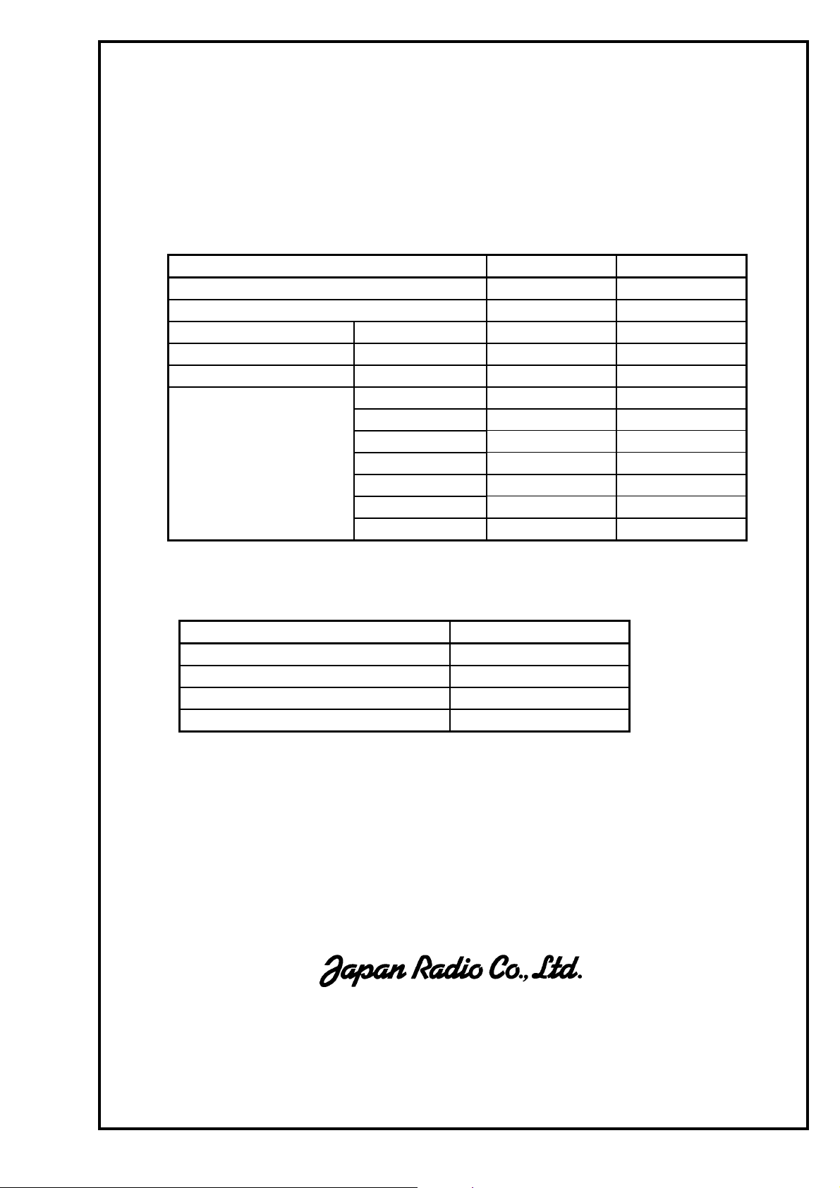
Electrical Specification: (Table 1)
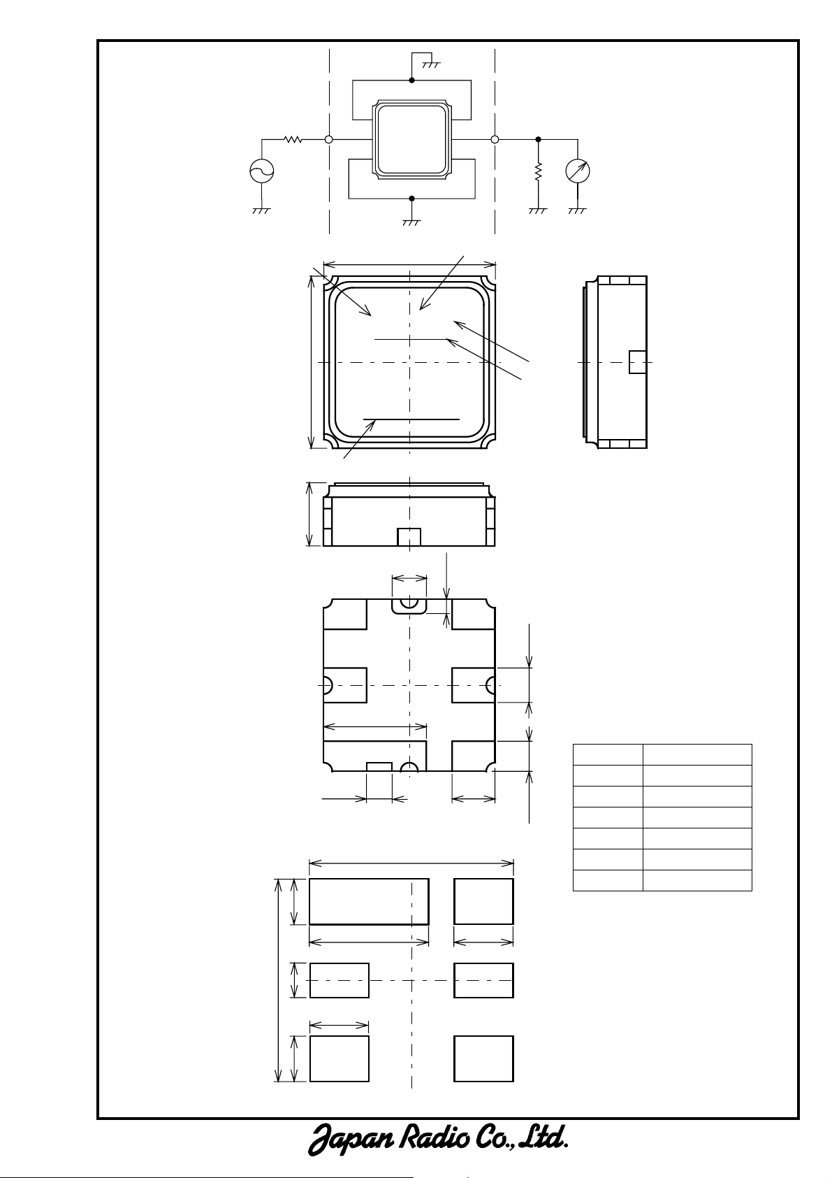
The device characteristics are measured in the circuit shown in Fig.1.
Maximum Rating: (Table 2)
Mechanical Specifications: (Fig.2)
Package is designed as small as 3.0x3.0x1.15[mm
Notice:
This part is electrostatic discharge sensitive and may be damaged by improper handling.
915MHz ISM
Table 1. Electrical Specifications
Item Spec. Typ.
Input and Output Impedance Nominal Center Frequency (f0) - 915MHz
Insertion Loss 902.0~928.0MHz 4.0dB max. 3.0dB
Response Variation 902.0~928.0MHz 2.0dB max. 1.0dB
Input and Output VSWR 902.0~928.0MHz 2.5 max. 2.0
Out of Band Rejection
(Relative to
Through Level)
Table 2. Maximum Ratings
Item Rating
Maximum Input Power +10dBm
Maximum DC Voltage 7.5V
Operating Temperature Range -40~+85ºC
Storage Temperature -40~+85ºC
http://www.jrc.co.jp/jp/product/device/saw/index.html(Japanese)
JRC SAW FILTER
NSVS1240
DC~800MHz 40dB min. 48dB
800~880MHz 35dB min. 40dB
880~890MHz 25dB min. 30dB
940~960MHz 25dB min. 30dB
960~1080MHz 30dB min. 35dB
1080~1500MHz 35dB min. 38dB
1500~3000MHz 20dB min. 24dB
(Operating Temperature Range: -40~+85ºC)
3
] for SMD (Surface Mount Device) type.
Communications Equipment Division
Communications Equipment Marketing Department
10-1, Nishi-Shinjuku 6-chome, Shinjuku-ku,
Tokyo, 160-8328 Japan
Tel. +81 3-3348-3845
Fax. +81 3-3348-3935
http://www.jrc.co.jp/eng/product/saw/index.html(English)
50Ω
NSVS1240 Oct. 2008
IN
50Ω
1
2
34
SAW
6
5
OUT
50Ω
(a)
Fig.1 Measuring circuit
3. 0±0. 15
(b)
3. 0±0. 15
8X1
(c)
(1)
YX
3.8
(2)
1. 1 5±0. 15
(0.6)
(0.25)
3
2
(1.80)
1
(0.45)
Fig.2 Package dimensions (in mm)
3.8
0.93
2.2
0.6
1.15
(0. 75)
[4x]
1.15
Marking
(1) Lot Number
(a) Year
(b) Month
*Oct.--- X
Nov.--- Y
Dec.--- Z
4
(0.6)
5
6
(0.53)
(c) Date
*1-9--- 0
[2x]
10-19--- 1
20-31--- 2
(2) Part Number Mark
Pin no. Connection
1 GND
[4x]
2 IN
3 GND
4 GND
5 OUT
6 GND
0.93
Fig.3 Desirable land area (in mm)
 Loading...