

JRC NSVS1149 User Manual
NSVS1149 Apr. 2005
Application
Electrical Specification: (Table 1)
The device characteristics are measured in the circuit shown in Fig.2.
Table 1. Electrical Specifications (@25ºC)
Item Specification Typical
Center frequency Absolute frequency - 433.92 MHz
Tolerance from 433.92MHz Insertion Loss @Minimum Loss 2.5 dB max. Temperature Stability Turnover Temperature - 30 ºC
Temperature Coefficient - -0.03 ppm/ºC2
DC Insulation Resistance between any two terminals 1.0M ohm min RF Equivalent Motional Resistance (RM) - 14.0 ohm
RLC Model (fig.1) Motional Inductance (LM)-
Motional Capacitance (CM) - 2.925 fF
Shunt Static Capacitance (C0) - 1.65 pF
Maximum Rating: (Table 2)
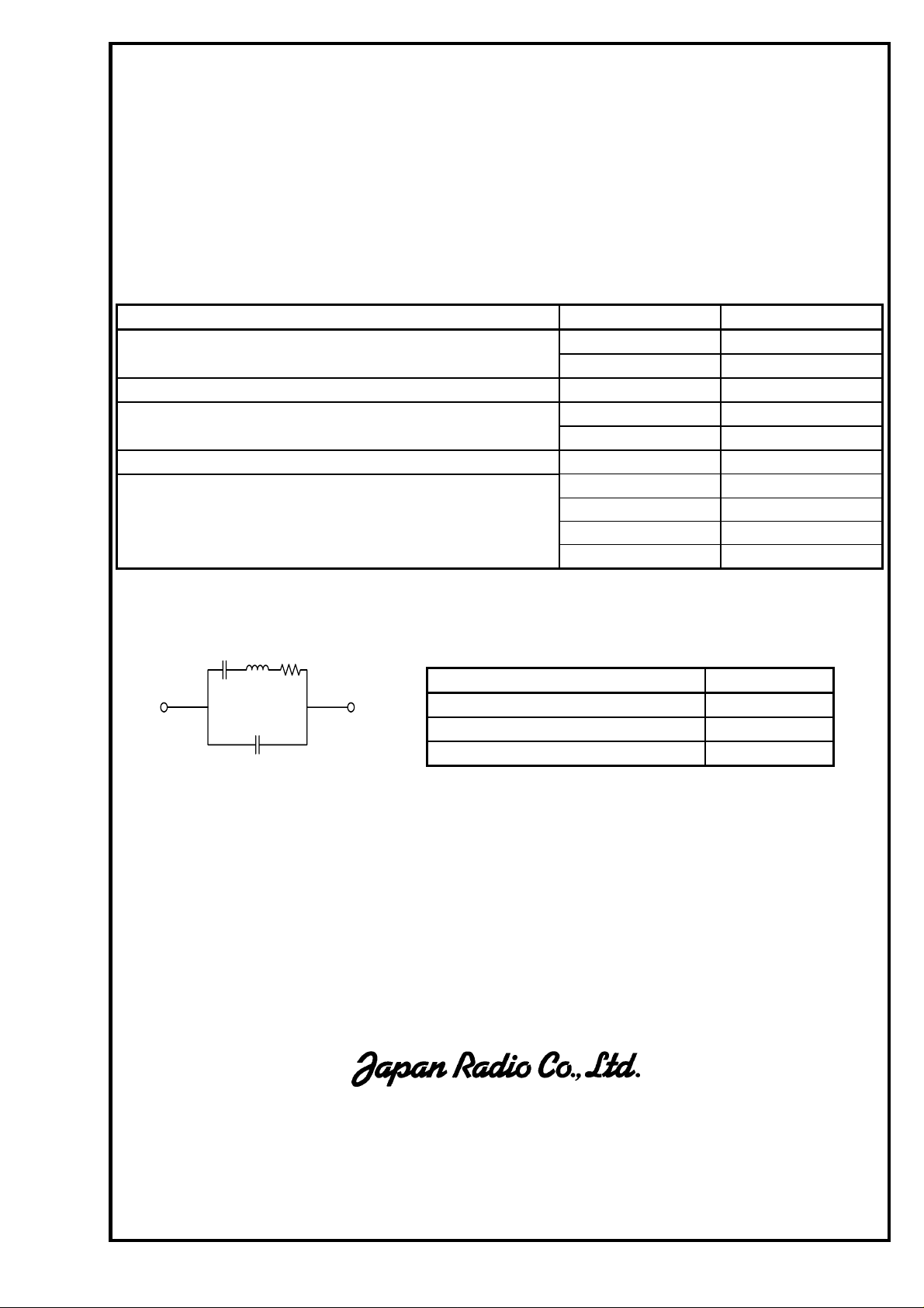
Fig.1 RF Equivalent RLC Model
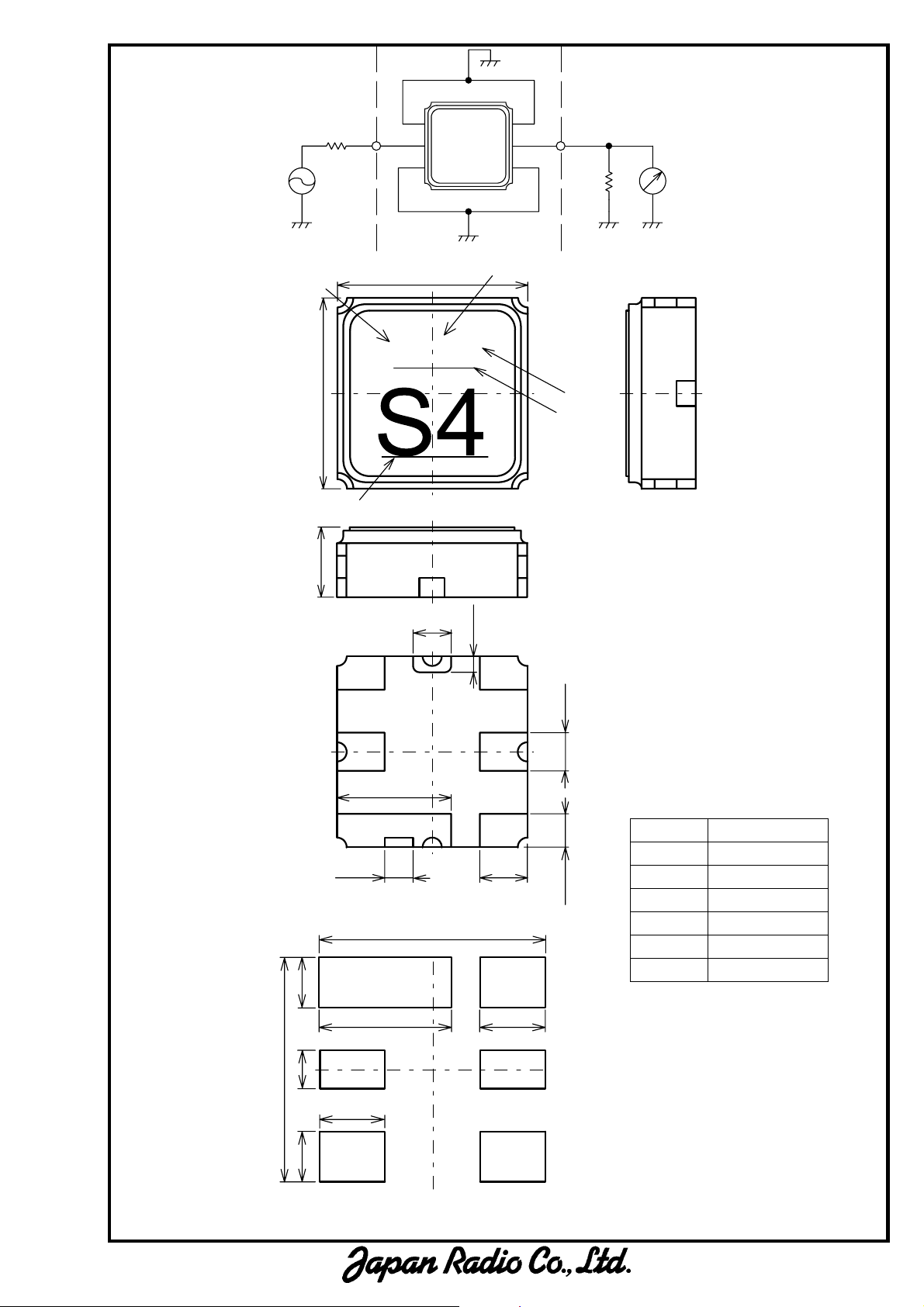
Mechanical Specifications: (Fig.2)
Package is designed as small as 3.0x3.0x1.15[mm
Notice:
This part is electrostatic discharge sensitive and may be damaged by improper handling.
433.92MHz Resonator
CM LM RM
JRC STW RESONATOR
NSVS1149
Table2. Maximum Ratings
Item Rating
Maximum Input Power 0dBm
C0
Communications and Device Group
Communications Equipment Marketing Department
10-1, Nishi-Shinjuku 6-chome, Shinjuku-ku,
http://www.jrc.co.jp/jp/product/device/saw/index.html (Japanese)
http://www.jrc.co.jp/eng/product/saw/index.html (English)
Operating Temperature Range -30~+80ºC
Storage Temperature -40~+85ºC
3
] for SMD (Surface Mount Device) type.
Tokyo, 160-8328 Japan
Tel. +81 3-3348-3845
Fax. +81 3-3348-3935
±100kHz
46.0 μH
NSVS1149 Apr. 2005
IN
50Ω
1
2
34
SAW
6
5
OUT
50Ω
(a)
Fig.1 Measuring circuit
3. 0±0. 15
(b)
3. 0± 0. 15
540
(c)
(1)
(2)
Marking
(1) Lot Number
1. 15± 0.15
(0. 6)
(0.25)
3
2
(1. 80)
4
[2x]
(0.6)
5
(a) Year
(b) Month
*Oct.--- X
Nov.--- Y
Dec.--- Z
(c) Date
1-9--- 0
10-19--- 1
20-31--- 2
(2) Part Number Mark
1
(0. 45)
Fig.2 Package dimensions (in mm)
3.8
0.93
(0. 75)
[4x]
6
[4x]
(0.53)
Pin no. Connection
1 GND
2 IN/OUT
3 GND
4 GND
5 OUT/IN
6 GND
2.2
1.15
0.6
3.8
1.15
0.93
Fig.3 Desirable land area (in mm)
 Loading...