

NJW1138
PRELIMINALY
AUDIO PROCESSOR
■■■■ GENERAL DESCRIPTION ■■■■ PACKAGE OUTLINE
The NJW1138 is an audio processor. It includes all of
functions processing audio signal for TV, such as tone
control, balance, vo lum e, m ute, NJRC origin al surr ound, an d
AGC functions.
The NJRC original surround system reproduces natural
surround sound and clear vocal orientation.
All of internal status and variables are controlled by I
BUS interface.
■■■■ FEATURES
●●●● Operating Voltage 8 to 13V
2
C BUS Interface
●●●● I
●●●● AGC Circuit (It reduces volume difference among input sources.)
●●●● eala(NJRC Original Surround)
●●●● Simulated Surround
●●●● Bi-CMOS Technology
●●●● Package Outline SDIP30, SDMP30
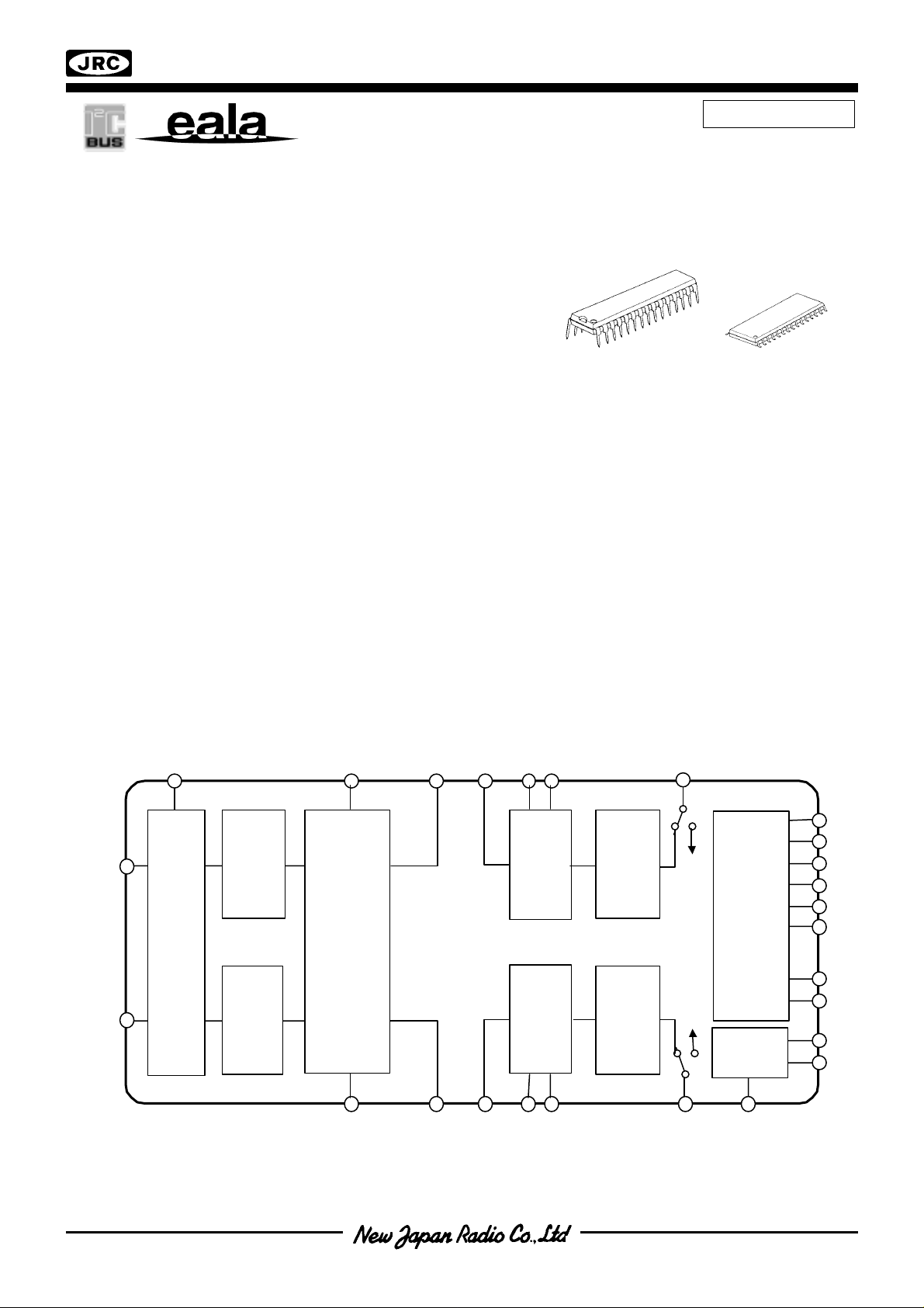
■■■■ BLOCK DIAGRAM
2
C
NJW1138M NJW1138L
VOL1
TONE
eala
AGC
&
Simulated
Surround
VOL2
I2C Bus
Interface
VOL1
TONE
VOL2
Bias
- 1 –F

NJW1138
A
A
A
A
■■■■ PIN FUNCTION
INa
NC
NC
OUT1a
IN2a
TONE-Ha
TONE-La
OUT2a
GC
SS-FIL
CVB
CV
SDA
INb
NC
NC
OUT1b
IN2b
TONE-Hb
TONE-Lb
OUT2b
SR-FIL
VREF
CTH
CTL
UX0
SCL
GND
UX1
Vcc
No. Symbol Function No Symbol Function
1 IN1a Ach Input 16 Vcc Power Supply Pin
2 NC Non Connect 17 AUX1 Auxiliary Output1
3 NC Non Connect 18 AUX0 Auxiliary Output0
4 OUT1a Ach Output for the Other Accessories 19 CTL DAC Output for Tone Low Frequency
5 IN2a Ach Input From the Other Accessories 20 CTH DAC Output for Tone High Frequency
6 TONE-Ha Ach Treble Filter 21 VREF Reference Voltage
7 TONE-La Ach Bass Filter 22 SR-FI L NJRC Original Surround Filter
8 OUT2a Ach Output 23 OUT2b Bch Output
9 AGC AGC Filter 24 TONE-Lb Bch Bass Filter
10 SS-FIL Simulated Stereo Filter 25 TONE-Hb Bch Treble Filter
11 CVB DAC Output for Bch Volume & Balance 26 IN2b Bch Input from the Other Accessories
12 CVA DAC Output for Ach Volume & Balance 27 OUT1b Bch Output for the Other Accessories
13 SDA SDA Data Input (I2C BUS) 28 NC Non Connect
14 SCL SCL Data Input (I2C BUS) 29 NC Non Connect
15 GND GND 30 IN1b Bch Input
- 2 -

NJW1138
■■■■ ABSOLUTE MAXIMUM RATING (Ta=25°C)
PARAMETER SYMBOL RATING UNIT
Supply Voltage V+ 14 V
Power Dissipation PD 700 mW
Operating Temperature Range Topr -20 to +75 °C
Storage Temperature Range Tstg -40 to +125 °C
■■■■ ELECTRICAL CHARACTERISTICS
( Ta=25°C, V+=9V, Rg=600Ω, R
PARAMETER SYMBOL TEST CONDITION MIN. TYP. MAX. UNIT
Operating Voltage V+ 8.0 9.0 13.0 V
Supply Current ICC No Signal - 10 25 mA
Reference Voltage V
Maximum Input Voltage VIM VOL=-20dB,THD=1% 2.8 3.0 - Vrms
Maximum Output Voltage VOM
Channel Balance GCB VOL=0dB -1.5 0.0 1.5 dB
Balance Boost A BA
Balance Cut A BA
Balance Boost B BB
Balance Cut B BB
Total Harmonic Distortion THD
Maximum Gain G
Minimum Gain G
Channel Separation CS Vin = 2Vrms - - -70 dB
Output Noise 1 V
Output Noise 2 V
AUX Output Voltage V
=47kΩ, Vin=100mVrms/1kHz unless otherwise specified)
L
No Signal 4.0 4.5 5.0 V
REF
OUTPUT
VOL=0dB,THD=1%
CHS=”0”,BAL=”11111” -2.0 0.0 2.0 dB
BST
CHS=”1”,BAL=”11111”
CUT
BST
CUT
Vin = 1Vrms
CHS=”1”,BAL=”11111” -2.0 0.0 2.0 dB
CHS=”0”,BAL=”11111”
Vin = 1Vrms
Vo=0.5Vrms
BW=400Hz to 30kHz
VOL= 0dB -2.0 0.0 2.0 dB
VMAX
VOL= MUTE - - -70 dB
VMIN
VOL = 0dB
NO1
NO2
BW=400Hz to 30kHz
VOL = MUTE
BW = 400Hz to 30kHz
- 2.5 - Vrms
- - -70 dB
- - -70 dB
- - 0.5 %
-
-
(31.6)
-
-
Logic Output : High 4.5 - 5.0
AUX
Logic Output : Low 0 - 0.3
-90
-106
(5.0)
-85
(56.2)
-96
(15.8)
dBV
(µVrms)
dBV
(µVrms)
V
BW : Band Width
-3-

NJW1138
♦♦♦♦ TONE CONTROL
PARAMETER SYMBOL TEST CONDITION MIN. TYP. MAX. UNIT
High Frequency Boost HF
High Frequency Flat HF
High Frequency Cut HF
Low Frequency Boost LF
Low Frequency Flat LF
Low Frequency Cut LF
♦♦♦♦ SUB-TONE CONTROL
PARAMETER SYMBOL TEST CONDITION MIN. TYP. MAX. UNIT
High Frequency Boost SHF
High Frequency Cut SHF
Low Frequency Boost SLF
Low Frequency Cut SLF
BST
FLT
CUT
BST
FLT
CUT
f=10kHz
TRBE=”0000”,f=10kHz -2.0 0.0 2.0 dB
BCT=”0”,TRBE=”1111”,
f=10kHz
BCB=”1”,BASS=”1111”,
f=100Hz
BASS=”0000”,f=100Hz -2.0 0.0 2.0 dB
BCB=”0”,BASS=”1111”,
f=100Hz
BCST=”1”,
BST
SUB-TREB=”11”,f=10kHz
BCST=”0”,
CUT
SUB-TREB=”11”,f=10kHz
BCSB=”1”,
BST
SUB-BASS=”11”,f=100Hz
BCSB=”0”,
CUT
SUB-BASS=”11”,f=100Hz
BCT=”1”,TREB=”1111”,
12.5 15.0 17.5 dB
-17.5 -15.0 -12.5 dB
12.5 15.0 17.5 dB
-17.5 -15.0 -12.5 dB
2.0 3.0 4.0 dB
-4.0 -3.0 -2.0 dB
2.0 3.0 4.0 dB
-4.0 -3.0 -2.0 dB
♦♦♦♦ AGC CONTROL(AGC-ON)
PARAMETER SYMBOL TEST CONDITION MIN. TYP. MAX. UNIT
AGC Boost AGC
AGC Flat1 AGC
AGC Flat2 AGC
AGC Flat3 AGC
AGC Flat4 AGC
AGC Cut AGC
♦♦♦♦ SURROUND (SURROUND-ON)
PARAMETER SYMBOL TEST CONDITION MIN. TYP. MAX. UNIT
Surround Gain1 SR
Surround Gain2 SR
Surround Gain3 SR
Surround Gain4 SR
Simulated Surround Gain1 SR
Simulated Surround Gain2 SR
Vin=50mVrms, f=1kHz 1.5 3.5 5.5 dB
BST
Vin=150mVrms, f=1kHz -2.5 0.0 2.5 dB
FLT1
Vin=300mVrms, f=1kHz -2.5 0.0 2.5 dB
FLT2
Vin=400mVrms, f=1kHz -2.5 0.0 2.5 dB
FLT3
Vin=540mVrms, f=1kHz -2.5 0.0 2.5 dB
FLT4
Vin=2Vrms, f=1kHz -14 -10 -6.0 dB
CUT
GAIN1
GAIN2
GAIN3
GAIN 4
SIM1
SIM2
Ain→Aout, f=100Hz
SUR0=”0”, SUR=”1”
Ain→Bout, f=100Hz
SUR0=”0”, SUR=”1”
Ain→Aout, f=100Hz
SUR0=”1”, SUR=”1”
Ain→Bout, f=100Hz
SUR0=”1”, SUR=”1”
Ain+Bin→Aout, f=1kHz
SUR0=”1”, SUR=”0”
Ain+Bin→Bout, f=1kHz
SUR0=”1”, SUR=”0”
6.0 8.0 10.0
1.6 3.6 5.6
10.7 12.7 14.7
8.4 10.4 12.4
1.0 3.0 5.0
1.0 3.0 5.0
dB
dB
dB
dB
dB
dB
- 4 -

P
S
P
NJW1138
2
■■■■ I
C BUS BLOCK CHARACTERISTICS (SDA,SCL)
PARAMETER SYMBOL MIN. TYP. MAX. UNIT
High Level Input Voltage VIH 3.0 - 5.0 V
Low Level Input Voltage VIL 0 - 1.5 V
High Level Input Current IIH - - 10 µA
Low Level Input Current IIL - - 10 µA
Low Level Output Voltage (3mA at SDA pin) VOL 0 - 0.4 V
Maximum Output Current IOL -3.0 - - mA
Maximum Clock Frequency f
Data Change Minimum Waiting Time t
Data Transfer Start Minimum Waiting Time t
Low Level Clock Pulse Width t
High Level Clock Pulse Width T
Minimum Start Preparation Waiting Time t
Minimum Data Hold Time t
Minimum Data Preparation Time t
0 - 100 kHz
SCL
4.7 - - µs
BUF
4.0 - - µs
HD:STA
4.7 - - µs
LOW
4.0 - - µs
HIGH
4.7 - - µs
SU:STA
5.0 - - µs
HD:DAT
250 - - ns
SU:DAT
Rise Time tR - - 1.0 µs
Fall Time tF - - 300 ns
Minimum Stop Preparation Waiting Time t
2
C BUS Load Condition: Pull up resistance 4kΩ (Connected to +5V)
I
4.7 - - µs
SU:STO
Load capacitance 200pF (Connected to GND)
SDA
SCL
t
LOW
tR
t
HD:DA
t
BU
t
HD:ST
t
HIGH
tF
t
HD:ST
t
t
SU:DA
SU:ST
t
SU:ST
Sr
-5-

NJW1138
TERMINAL DESCRIPTION
No. SYMBOL FUNCTION EQUIVALENT CIRCUIT VOLTAGE
V+
1
30
4
8
23
27
10 SS-FIL
INa
INb
OUT1a
OUT2a
OUT2b
OUT1b
Ach Input terminal
Bch Input terminal
Ach Output for the Other Accessories
Bch Output for the Other Accessories
Simulated Stereo Filter
Ach Output
Bch Output
terminal
1,30 pin
20k
V+/2
80k
Vref
FB
50
4, 8
23,27pin
V+/2
5.3 k
FB
10pin
V+/2
6
25
TONE-Ha
TONE-Hb
Treble(tone control) filter terminal
FB
10k
6, 25pin
V+/2
7
24
TONE-La
TONE-Lb
Bass(tone control) filter terminal
12k
FB
12k
7, 24pin
V+/2
- 6 -

TERMINAL DESCRIPTION
NJW1138
No. SYMBOL FUNCTION EQUIVALENT CIRCUIT VOLTAGE
9 AGC
11
12
13 SDA
CVB
CVA
Capacitor connection terminal for
AGC attack and recovery time setting
DAC output terminal for Bch volume control
DAC output terminal for Ach volume control
I2C data terminal
11,12pin
400
5V
4k
400
4k
9pin
-
-
13pin
8k
-
14 SCL
5
TONE INa
26
TONE INb
I2C clock terminal
Ach Input from the Other Accessories
Bch Input from the Other Accessories
5V
4k
-
14pin
8k
5,26pin
24k
V+/2
-7-

NJW1138
TERMINAL DESCRIPTION
No. SYMBOL FUNCTION EQUIVALENT CIRCUIT VOLTAGE
21 Vref
17
18
20
19
AUX0
AUX1
CTH
CTL
Reference voltage terminal
Auxiliary 2 values voltage output terminal
DAC output for tone control terminal
21pin
19pin
5V
200k
36k
V+/2
17,18pin
0/5V
-
22 SR-FIL
15
16
V+
GND
filter terminal
eala
Ground terminal
Supply voltage terminal
FB
1.8k
- -
22pin
V+/2
- 8 -

A
A
■■■■ APPLICA TION CIRCUIT
NJW1138
4.7n
100n
1µ
100n
4.7µ
4.7µ
4.7µ
4.7µ
4.7µ
IN1a
1 30
2
NC
NC
3
4
OUT1a
5
IN2a
6
TONE-Ha
7
TONE-La
OUT2a
8
AGC
9
SS-FIL
10
CVB
11
IN1b
NC
NC
OUT1b
IN2b
TONE-Hb
TONE-Lb
OUT2b
SR-FIL
VREF
CTH
29
28
27
26
25
24
23
22
21
20
4.7µ
4.7µ
4.7µ
4.7n
100n
4.7µ
100n
4.7µ
4.7µ
4.7µ
12
13
14
15
CVA
SDA
SCL
GND
CTL
UX0
UX1
Vcc
19
18
17
16
22µ
4.7µ
-9-

NJW1138
■■■■ DEFINITION OF I2C REGISTER
2
♦♦♦♦ I
C BUS FORMAT
MSB LSB MSB LSB MSB LSB
S Slave Address A Select Addr ess A Data A P
1bit 8bit 1bit 8bit 1bit 8bit 1bit 1bit
S: Starting Term
A: Acknowledge Bit
P: Ending Term
♦♦♦♦ SLAVE ADDRESS
MSB LSB
1 0 0 0 0 0 1 R/W
R/W=0: Receive Only
R/W=1: No Output Data
♦♦♦♦ CONTROL REGISTER TABLE
The select address sets each function (Volume, Balance, AGC, Surround, Tone Control, AUX).
The auto increment function cycles the select address as follows.
00H→01H→02H→03H→04H→05H→00H
Select
Address
D7 D6 D5 D4 D3 D2 D1 D0
BIT
00H
01H
02H
03H
(✴)
04H
05H
(✴)
♦♦♦♦ CONTROL REGISTER DEFAULT VALUE
Control register default value is all “0”.
Select
Address
00H
01H
02H
03H
04H
CHS BAL AGC SUR
BCB BASS BCSB SUB-BASS
BCT TREB BCST SUB-TREB
0 0 0 0 0 0 0 0
OUT
Don’t care Don’t care
D7 D6 D5 D4 D3 D2 D1 D0
0 0 0 0 0 0 0 0
0 0 0 0 0 0 0 0
0 0 0 0 0 0 0 0
0 0 0 0 0 0 0 0
0 0 0 0 0 0 0 0
VOL
SUR0 AGC1 AGC0 AUX1 AUX0
BIT
Please send the data only “0”
05H
- 10 -
0 0 0 0 0 0 0 0

NJW1138
INSTRUCTION CODE
a) MASTER VOLUME SETTING
Select
Address
00H
D7 D6 D5
BIT
D4 D3 D2 D1 D0
VOL
The volume control for both Ach and Bch(0.33dB/step).
The volume is consisted of volume1 and volume2 and the le vel is divided into half to each volum e1 and
volume2.
b) BALANCE, AGC AND SURROUND SETTING
Select
Address
01H
D7 D6 D5
CHS BAL AGC SUR
BIT
D4 D3 D2 D1 D0
•CHS : Channel select for balance control
“0” : Ach “Bch is attenuated”
“1” : Bch “Ach is attenuated”
•BAL : Balance control for both Ach and Bch(1dB/Step)
The balance is consiste d of volume1 and volume2 and the level is div ided into half to each volume1 and
volume2.
•AGC : AGC switch
“0” : AGC OFF
“1” : AGC ON (Default Setting : 150mVrms)
•SUR : Surround mode switch
“0” : Surround OFF
“1” : Surround ON(Default Setting : Surround Effect1)
c)TONE CONTROL BASS SETTING
Select
Address
02H
D7 D6 D5
BCB BASS BCSB SUB-BASS
BIT
D4 D3 D2 D1 D0
•BCB : Boost cut select for Bass control
“0” : Cut
“1” : Boost
•BASS: BASS control
Cut Level : -15dB to 0dB(1dB/Step)
Boost Level : 0dB to +15dB(1dB/Step)
•BCSB : Boost cut select for SUB-BASS control
“0” : Cut
“1” : Boost
•SUB-BASS: SUB- BASS c ontrol(1dB/Step)
Sub-Cut Level : -3dB to 0dB(1dB/Step)
Sub-Boost Level : 0dB to +3dB(1dB/Step)
- 11 -

NJW1138
d) TONE CONTROL TREBLE SETTING
Select
Address
03H
D7 D6 D5
BCT TREB BCST SUB-TREB
•BCT : Boost cut select for Treble control
“0” : Cut
“1” : Boost
•TREB: Treble control(1dB/step)
Cut Level : -15dB to 0dB(1dB/Step)
Boost Level : 0dB to +15dB(1dB/Step)
•BCST : Boost cut select for Sub-Treble control
“0” : Cut
“1” : Boost
•SUB-TREB: Sub-Treble control( 1dB /s tep)
Sub-Cut Level : -3dB to 0dB(1dB/Step)
Sub-Boost Level : 0dB to +3dB(1dB/Step)
e)OUTPUT AND AUXILIARY SETTING
Select
Address
05H
D7 D6 D5
OUT
Don’t Care Don’t Care
•OUT: ON/OFF Switch for OUTPUT
“0” : OFF
“1” : ON
•Surround Setting
Surround Function SUR0(05H:D4) SUR(01H:D0), Remarks
Surround OFF 0 0 Surround OFF
Surround Effect1 0 1 Surround Effect Small ( 8.0dB typ. )
Surround Effect2 1 1 Surround Effect Large (12.7dB typ. )
Simulated Stereo 1 0 Monaural to Stereo
•AGC Level Setting
AGC Level AGC1(D3) AGC0(D2)
150mVrms 0 0
300mVrms 0 1
400mVrms 1 0
540mVrms 1 1
•AUX1/AUX0: Auxiliary port High/Low
“0” : Logic output ”Low”
“1” : Logic output ”High”
BIT
D4 D3 D2 D1 D0
BIT
D4 D3 D2 D1 D0
SUR0 AGC1 AGC0 AUX1 AUX0
- 12 -

NJW1138
MASTER VOLUME (Select Address : 00H)
Gain(dB) HEX D7 D6 D5 D4 D3 D2 D1 D0
0 FF 1 1 1 1 1 1 1 1
-1 FC 1 1 1 1 1 1 0 0
-2 F9 1 1 1 1 1 0 0 1
-3 F6 1 1 1 1 0 1 1 0
-4 F3 1 1 1 1 0 0 1 1
-5 F0 1 1 1 1 0 0 0 0
-6 ED 1 1 1 0 1 1 0 1
-7 EA 1 1 1 0 1 0 1 0
-8 E7 1 1 1 0 0 1 1 1
-9 E4 1 1 1 0 0 1 0 0
-10 E1 1 1 1 0 0 0 0 1
-11 DE 1 1 0 1 1 1 1 0
-12 DB 1 1 0 1 1 0 1 1
-13 D8 1 1 0 1 1 0 0 0
-14 D5 1 1 0 1 0 1 0 1
-15 D2 1 1 0 1 0 0 1 0
-16 CF 1 1 0 0 1 1 1 1
-17 CC 1 1 0 0 1 1 0 0
-18 C9 1 1 0 0 1 0 0 1
-19 C6 1 1 0 0 0 1 1 0
-20 C3 1 1 0 0 0 0 1 1
-21 C0 1 1 0 0 0 0 0 0
-22 BD 1 0 1 1 1 1 0 1
-23 BA 1 0 1 1 1 0 1 0
-24 B7 1 0 1 1 0 1 1 1
-25 B4 1 0 1 1 0 1 0 0
-26 B1 1 0 1 1 0 0 0 1
-27 AE 1 0 1 0 1 1 1 0
-28 AB 1 0 1 0 1 0 1 1
-29 A8 1 0 1 0 1 0 0 0
-30 A5 1 0 1 0 0 1 0 1
-31 A2 1 0 1 0 0 0 1 0
-32 9F 1 0 0 1 1 1 1 1
-33 9C 1 0 0 1 1 1 0 0
-34 99 1 0 0 1 1 0 0 1
-35 96 1 0 0 1 0 1 1 0
-36 93 1 0 0 1 0 0 1 1
-37 90 1 0 0 1 0 0 0 0
-38 8D 1 0 0 0 1 1 0 1
-39 8A 1 0 0 0 1 0 1 0
-40 87 1 0 0 0 0 1 1 1
-41 84 1 0 0 0 0 1 0 0
-42 81 1 0 0 0 0 0 0 1
VOL
- 13 -

NJW1138
MASTER VOLUME (Select Address : 00H)
Gain(dB) HEX D7 D6 D5 D4 D3 D2 D1 D0
-43 7E 0 1 1 1 1 1 1 0
-44 7B 0 1 1 1 1 0 1 1
-45 78 0 1 1 1 1 0 0 0
-46 75 0 1 1 1 0 1 0 1
-47 72 0 1 1 1 0 0 1 0
-48 6F 0 1 1 0 1 1 1 1
-49 6C 0 1 1 0 1 1 0 0
-50 69 0 1 1 0 1 0 0 1
-51 66 0 1 1 0 0 1 1 0
-52 63 0 1 1 0 0 0 1 1
-53 60 0 1 1 0 0 0 0 0
-54 5D 0 1 0 1 1 1 0 1
-55 5A 0 1 0 1 1 0 1 0
-56 57 0 1 0 1 0 1 1 1
-57 54 0 1 0 1 0 1 0 0
-58 51 0 1 0 1 0 0 0 1
-59 4E 0 1 0 0 1 1 1 0
-60 4B 0 1 0 0 1 0 1 1
-61 48 0 1 0 0 1 0 0 0
-62 45 0 1 0 0 0 1 0 1
-63 42 0 1 0 0 0 0 1 0
-64 3F 0 0 1 1 1 1 1 1
-65 3C 0 0 1 1 1 1 0 0
-66 39 0 0 1 1 1 0 0 1
-67 36 0 0 1 1 0 1 1 0
-68 33 0 0 1 1 0 0 1 1
-69 30 0 0 1 1 0 0 0 0
-70 2D 0 0 1 0 1 1 0 1
-71 2A 0 0 1 0 1 0 1 0
-72 27 0 0 1 0 0 1 1 1
-73 24 0 0 1 0 0 1 0 0
-74 21 0 0 1 0 0 0 0 1
-75 1E 0 0 0 1 1 1 1 0
-76 1B 0 0 0 1 1 0 1 1
-77 18 0 0 0 1 1 0 0 0
-78 15 0 0 0 1 0 1 0 1
-79 12 0 0 0 1 0 0 1 0
-80 0F 0 0 0 0 1 1 1 1
-81 0C 0 0 0 0 1 1 0 0
-82 09 0 0 0 0 1 0 0 1
-83 06 0 0 0 0 0 1 1 0
-84 03 0 0 0 0 0 0 1 1
Mute 00 0 0 0 0 0 0 0 0
VOL
- 14 -

BALANCE(Select Address : 01H)
Channel
Select (CHS)
Ach(Bch is attenuated) 0
Bch(Ach is attenuated) 1
NJW1138
D7
Gain(dB) D6 D5 D4 D3 D2
0 0 0 0 0 0
-1 0 0 0 0 1
-2 0 0 0 1 0
-3 0 0 0 1 1
-4 0 0 1 0 0
-5 0 0 1 0 1
-6 0 0 1 1 0
-7 0 0 1 1 1
-8 0 1 0 0 0
-9 0 1 0 0 1
-10 0 1 0 1 0
-11 0 1 0 1 1
-12 0 1 1 0 0
-13 0 1 1 0 1
-14 0 1 1 1 0
-15 0 1 1 1 1
-16 1 0 0 0 0
-17 1 0 0 0 1
-18 1 0 0 1 0
-19 1 0 0 1 1
-20 1 0 1 0 0
-21 1 0 1 0 1
-22 1 0 1 1 0
-23 1 0 1 1 1
-24 1 1 0 0 0
-25 1 1 0 0 1
-26 1 1 0 1 0
-27 1 1 0 1 1
-28 1 1 1 0 0
-29 1 1 1 0 1
-30 1 1 1 1 0
Mute 1 1 1 1 1
BAL
- 15 -

NJW1138
TONE CONTROL BASS (Select Address : 02H)
Bass
Cut or Boost
Cut 0
Boost 1
BCB
D7
BASS
Cut Gain(dB) Boost Gain(dB) D6 D5 D4 D3
-15 15 1 1 1 1
-14 14 1 1 1 0
-13 13 1 1 0 1
-12 12 1 1 0 0
-11 11 1 0 1 1
-10 10 1 0 1 0
-9 9 1 0 0 1
-8 8 1 0 0 0
-7 7 0 1 1 1
-6 6 0 1 1 0
-5 5 0 1 0 1
-4 4 0 1 0 0
-3 3 0 0 1 1
-2 2 0 0 1 0
-1 1 0 0 0 1
0 0 0 0 0 0
TONE CONTROL SUB-BASS (Select Address : 02H)
BCSB Sub-Bass
Cut or Boost
Cut 0
Boost 1
D2
SUB-BASS
Cut Gain(dB) Boost Gain(dB) D1 D0
-3 3 1 1
-2 2 1 0
-1 1 0 1
0 0 0 0
- 16 -

TONE CONTROL TREBLE (Select Address : 03H)
BCT Treble
Cut or Boost
Cut 0
Boost 1
TREB
Cut Gain(dB)
-15 15 1 1 1 1
-14 14 1 1 1 0
-13 13 1 1 0 1
-12 12 1 1 0 0
-11 11 1 0 1 1
-10 10 1 0 1 0
-9 9 1 0 0 1
-8 8 1 0 0 0
-7 7 0 1 1 1
-6 6 0 1 1 0
-5 5 0 1 0 1
-4 4 0 1 0 0
-3 3 0 0 1 1
-2 2 0 0 1 0
-1 1 0 0 0 1
0 0 0 0 0 0
Boost
Gain(dB)
TONE CONTROL SUB-TREBLE (Select Address : 03H)
Cut or Boost
Cut 0
Boost 1
D7
D6 D5 D4 D3
BCST Sub-Treble
D2
NJW1138
Cut Gain(dB)
-3 3 1 1
-2 2 1 0
-1 1 0 1
0 0 0 0
SUB-TREB
Boost
Gain(dB)
D1 D1
- 17 -

NJW1138
TYPICAL CHARACTERISTICS
Supply Current vs Supply Voltage
Ta=25degC
15
Su pp ly Current vs T emp arature
V+=9V
16
NJW 1137
10
NJW 1138
5
Supply Cur re nt [m A]
0
0 5 10 15
Supply Current [Hz]
Reference V o ltag e vs S u pp ly V o ltage
Ta= 25 degC
8
6
4
14
12
10
Supply Cur re nt [m A]
NJW 1137
NJW 1138
8
6
0 50 100
Temp arature [degC]
Reference Vo ltag e vs T emparature
V+=9V
5
4.8
4.6
4.4
2
Reference V oltage [V]
0
0 5 10 15
Supp ly Voltage [V]
Gain vs V o lume C ontrol
V+=9V, V in(Ach)=1Vrms,f=1kHz,
OUTPUT,Rg=600ohm
0
-20
-40
-60
Gain [dB ]
-80
75,25,-20degC
-100
0 50 100 150 200 250
Volume Control [dec]
Reference V oltage [V]
4.2
4
050100
Temp arature [degC]
Gain vs Balance Control
V+=9V, Vin=1Vrms, f=1kHz, Rg=600ohm
0
-20
-40
Vo(Bch)
75, 25, -20degC
-60
Gain [dB ]
-80
-100
02550
B alance Contr ol [dec]
Vo(Ach )
75, 25, -20degC
- 18 -

TYPICAL CHARACTERISTICS
100
T.H.D .+N vs Inp u t Vo ltage
V+=9V, Vin(Ach), f=1kHz, Vo(Ach)OUTPUT
Rg=600ohm, BW=400Hz-30kHz, Ta=25degC
NJW1138
T.H.D .+N vs Inp u t Vo ltage
V+=9V, Vin(Ach), f=1kHz, Vo(Ach)OUTPUT
Rg=600ohm, BW=400 Hz-30kHz, Vol=-20dB
100
10
-30dB
1
THD+N [ % ]
0.1
-20dB
-10dB
0.01
0.01 0.1 1
0dB
Input Voltage [Vrms]
T.H.D+N vs O utput Voltage
V+=9V, Vin(Ach), f=1kHz, Vo(Ach)OUTPUT
Rg=600ohm, BW=400Hz-30kHz, Ta=25degC
100
10
-30dB
1
THD+N [ % ]
0.1
10
1
THD+N [ % ]
0.1
0.01
0.01 0.1 1
-20d e g C
Input Voltage [Vrms]
25degC
T.H.D+N vs O utput Voltage
V+=9V, Vin(Ach), f=1kHz , Vo(Ach)OUTPUT
Rg=600ohm, BW =400Hz-30kHz, Vol=0dB
100
10
1
THD+N [ % ]
0.1
-20deg C
25degC
75degC
0.01
0.01 0.1 1
-20dB
Ou tput Vo ltage [V r ms]
-10dB
Channel Separation vs Frequency
V+=9V, Vin=2Vrms, f=1kHz, Vo=OUTPUT
Rg=600ohm, Vol=0dB, Ta=25degC
100
80
60
Vin(Ach)-Vo(B ch )
40
Channel Separation [Hz]
20
0
100 1000 10
Vin(Bch)-Vo(A ch )
Freqency [Hz]
0dB
75degC
0.01
0.01 0.1 1
Ou tput Vo ltage [V r ms]
Gain vs Frequency (MUT E)
V+=9V, Vin(Ach)=1Vrms, Vol=MUTE
Vo(Ach)OUTPUT, Rg=600ohm, Ta=25degC
120
100
80
60
Gain [Hz]
40
20
4
0
100 1000 10
Frequency [Hz]
4
- 19 -

NJW1138
TYPICAL CHARACTERISTICS
AGC Control
V+=9V, Vin(Ach+Bch ), f=1k Hz, Vo(Ach) OUTPUT
Rg=600ohm, Ta=25degC
Lv4
1
0.1
0.01
Output Vo ltage [Vrms]
0.001
0.001 0.01 0.1 1
Input Voltage [Vrms]
Lv3
Lv1 Lv2
OFF
AGC Attack T ime
V+=9V, Vin(Ach+Bch)=1Vrms,f=20kHz,Vo(Ach)OUTPUT
AGC level=0.15V,Rg=600 ohm,Ta=25degC
2
1.5
AGC Co ntro l
V+=9V, Vin(Ach+Bch), f=1kHz, Vo(Ach)OUTPUT
Rg=600ohm, Flat Level:0.15Vrms
1
0.1
0.01
Output Voltage [Vrms]
0.001
0.001 0.01 0.1 1
75, 25, -20degC
Input Voltage [Vrms]
AGC R e cove ry Ti me
V+=9V, Vin(Ach+Bch)=1Vrms, f=10kHz,Vo(Ach)OUTPUT
AGC level=0.15V,Rg=600ohm,Ta=25degC
0.2
0.15
1
0.5
0
-0.5
O u tpu t V o lt a g e [V]
-1
-1.5
-2
0246810
Time [msec]
Output Noise vs Temparature
V+=9V, Rg=600ohm, BW=400Hz- 30kHz
-40
-60
Vol=0dB
-80
0.1
0.05
0
-0.05
O u tpu t V o lt a g e [V]
-0.1
-0.15
-0.2
0 120 240 360 480 600
T ime [m se c]
Output Noise [dBV]
- 20 -
-100
-120
Vol=MUTE
0 50 100
Temp arature [degC]

TYPICAL CHARACTERISTICS
NJW1138
Gain vs Freque n cy (TON E )
V+=9V, Vin(Ach)=0.1Vrms,Gv:3dB steps
Vo(Ach), Rg=600ohm, Ta=25degC
20
10
0
Gain [dB]
-10
-20
100 1000 10
Frequen cy [Hz]
Gain v s Frequen cy (E ala & S i m ulated)
V+=9V, Vin(Ach)=0.1Vrms, Vo(Ach), Rg=600ohm
10
5
Sur1(Ain-Ao):75,25,-20degC
Gain vs Freq uency (T ON E)
V+=9V, Vin(Ach)=0.1Vrms,Gv=+15,0,-15dB
Vo(Ach), Rg=600ohm
20
+15dB
10
0
Gain [dB ]
-10
4
-20
-15dB
100 1000 10
Frequency [Hz]
75degC
25degC
-20degC
25degC
-20degC
75degC
4
SIM[(A+B)in-Aout]
:75,25,-20degC
0
Ga in [ d B ]
-5
Sur1(Bin-Ao):75,25,-20degC
-10
100 1000 10
Frequ e ncy [Hz]
■■■■NOTE
Purchase of I
conveys a license under the Ph ilips I
the system conforms to the I
2
C components of New Japan Radio Co., Ltd or one of its sublicensed Ass ociated Companies
2
C Standard Specification as defined by Philips.
4
2
C Patent Rights to use these com ponents in an I2C system, provide d tha t
[CAUTION]
The specifications on this databook are only
given for information , without any guarantee
as regards either mistakes or omissions. The
application circuits in this databook are
described only to show representati ve usages
of the product and not intended for the
guarantee or permission of any right including
the industrial rights.
- 21 -
 Loading...