

Y
查询NJW1136供应商
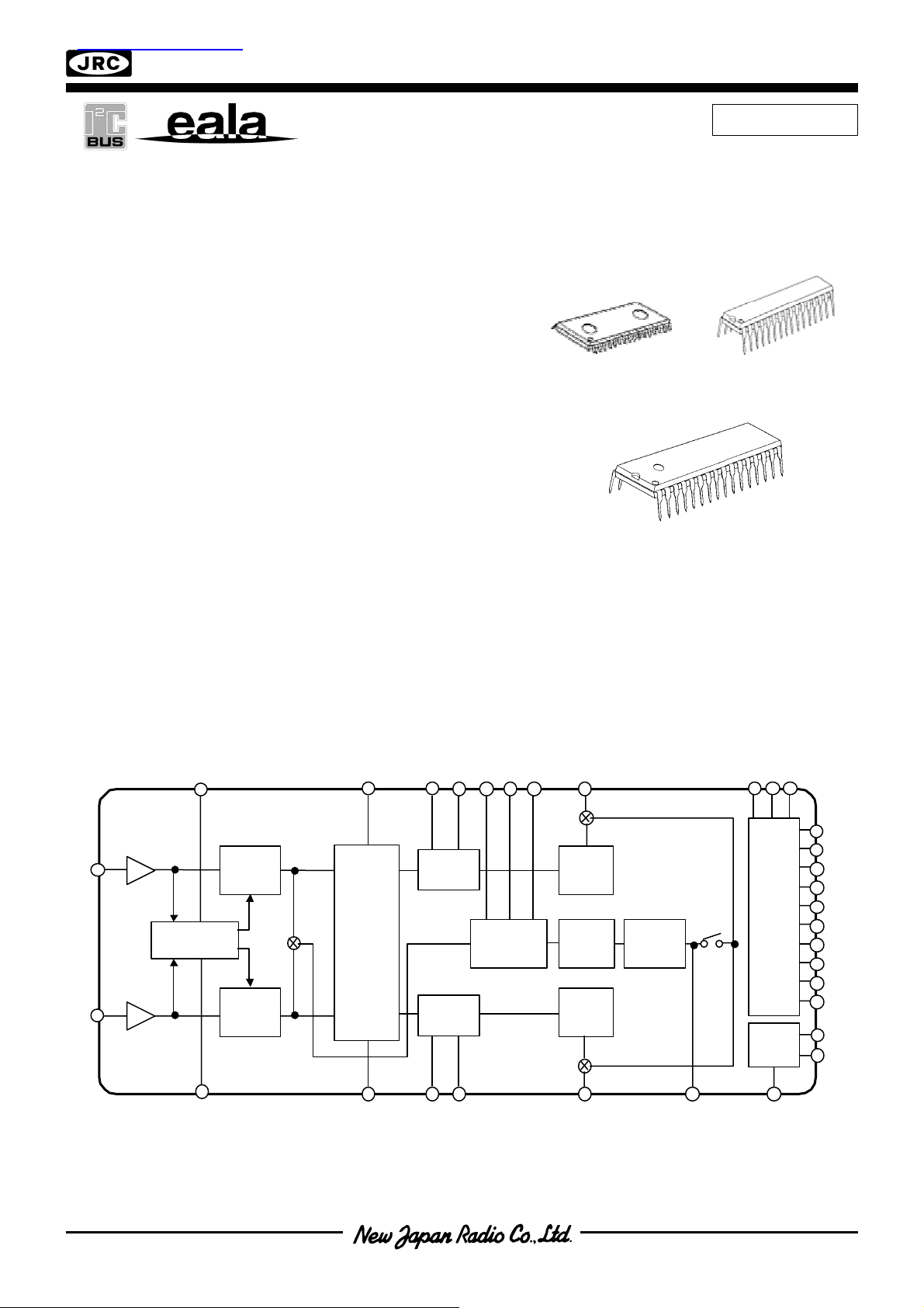
AUDIO PROCESSOR with Subwoofer Output
■■■■ GENERAL DESCRIPTION ■■■■ PACKAGE OUTLINE
The NJW1136 is a sound processor with subwoofer
output includes all of functions processing audio signal for
TV, such as tone control, balance, volume, mute, and AGC
functions.
Also the NJW1136 includes the LPF for subwoofer output
and bass boost function.
The original surround system reproduces natural surround
sound and clear vocal orientation.
All of internal status and variables are controlled by I
BUS interface.
■■■■ FEATURES
●●●● Operating Voltage 8 to 13V
●●●● 3ch Output(Lch, Rch, Subwoofer ch) / 2ch Output(Lch, Rch)
●●●● LPF Filter (Adjustable cut off frequency by external parts)
●●●● AGC Circuit (It reduces volume difference among input sources.)
Adjustable AGC boost level by external parts and AGC compression level by I
●●●● eala(NJRC Original Surround System)
●●●● Simulated Stereo
2
●●●● I
C BUS Interface
●●●● Bi-CMOS Technology
●●●● Package Outline SOP32, DIP32
■■■■ BLOCK DIAGRAM
AGC1
SS-FIL
TONE
-Ha
2
C
TONE
LF1 LF2 LF3 OUTa
-La
NJW1136D
2
C BUS
NJW1136
PRELIMINAR
NJW1136LNJW1136GL1
SCL SDA ADR
IN a
IN b
TONE VOL2
LPF
VOL2
I2CBUS
Int erf ace
Trimmer
AGC
VOL1
eal a
&
Simul ated
St ereo
VOL1
TONE
VOL2
Bia s
CVA
CVB
CVW
CTH
CTL
CSR
PORT1
PORT0
AUX1
AUX0
GND
V+
AGC2
SR-FIL TONE
-Hb
TONE
-Lb
OUTb OUTw
Vref
(1/24) G
NJW1136
(
A
A
A
A
A
A
A
f
■■■■PIN CONFIGURATION
INa
SR-FIL
INb
LF1
SS-FIL
LF2
TONE-Ha
LF3
TONE-La
TONE-Hb
OUTW
TONE-Lb
OUTa
OUTb
GC1
GC2
UX0
UX1
PORT0
PORT1
DR
CV
CVB
CVW
CTH
CTL
SD
SCL
GND
CSR
Vre
V+
No. Symbol Function No. Symbol Function
1 INa Ach input terminal 17 V+ Supply voltage terminal
2 SR-FIL Surround filter terminal 18 Vref Reference voltage terminal
3 SS-FIL Simulated stereo filter terminal 19 CSR DAC output terminal for surround control
4 TONE-Ha Ach tone control (treble) filter terminal 20 CTL DAC output terminal for tone control (bass)
5 TONE-La Ach tone control (bass) filter terminal 21 CTH DAC output terminal for tone control (treble)
6 OUTw Subwoofer output terminal 22 CVW Bch DAC output terminal for LPF trimmer
7 OUTa Ach output terminal 23 CVB Bch DAC output terminal for volume and balance
8 AGC1 AGC attack and recovery time setting terminal 24 CVA Ach DAC output terminal for volume and balance
Auxiliary 3 values voltage output terminal
9 AUX0
10 AUX1
11 PORT0 Logic input terminal 27 TONE-Lb Bch tone control (bass) filter terminal
12 PORT1 Logic input terminal 28 TONE-Hb Bch tone control (treble) filter terminal
13 ADR Slave address setting terminal 29 LF3 LPF filter3 terminal
14 SDA I2C data terminal 30 LF2 LPF filter2 terminal
15 SCL I2C cock terminal 31 LF1 LPF filter1 terminal
16 GND Ground terminal 32 INb Bch input terminal
(✳)
(0.0V, 2.5V, 5V)
Auxiliary 2 values voltage output terminal
(0.0V, V+)
25 AGC2 AGC boost level setting terminal
26 OUTb Bch output terminal
(✳)
The AUX0 terminal should be connected via the protection resistance to 5V device.
2/24)
(3/24)
NJW1136
■■■■ ABSOLUTE MAXIMUM RATING (Ta=25°C)
PARAMETER SYMBOL RATING UNIT
Supply Voltage V+ 15 V
Power Dissipation PD 700 mW
Operating Temperature Range Topr -20 to +75 °C
Storage Temperature Range Tstg -40 to +125 °C
■■■■ ELECTRICAL CHARACTERISTICS
( Ta=25°C, V+=9V, Rg=600Ω, R
PARAMETER SYMBOL
Operating Voltage V+ - - - 8.0 9.0 13.0 V
Supply Current1 I
Supply Current2 I
Reference Voltage V
Maximum Input Voltage1 V
Maximum Input Voltage2 V
Output Voltage1
Output Voltage2
Channel Balance GCB VOL=0dB - - - -1.5 0.0 1.5 dB
Balance Boost A BA
Balance Cut A BA
Balance Boost B BB
Balance Cut B BB
Trimmer Boost TR
Trimmer Cut TR
Total Harmonic Distortion THD
Maximum Gain G
Minimum Gain G
Channel Separation CS
Output Noise 1 V
Output Noise 2 V
=47kΩ, Vin=100mVrms/1kHz unless otherwise specified)
L
Condition
No Signal - - -
CC1
No Signal, V+=12V - - -
CC2
No Signal - - - 4.0 4.5 5.0 V
REF
VOL=-20dB,THD=1%
IM1
VOL=-20dB,THD=1%
IM2
V
OM1
V
OM2
V+=12V
VOL=0dB, THD=1%
VOL=0dB, THD=1%
V+=12V
CH S = ”0”,BA L = ” 111111” Vin Vin OUTa -2.0 0.0 2.0 dB
BST
CH S = ”1”, BA L = ” 111111”
CUT
Vin = 1Vrms
CH S = ”1”,BA L = ” 111111” Vin Vin OUTb -2.0 0.0 2.0 dB
BST
CH S = ”0”, BA L = ” 111111”
CUT
Vin = 1Vrms
VOL=0dB
BST
TRIM = +18dB
VOL=0dB
CUT
TRIM = -44dB
Vo=0.5Vrms,
BW=400Hz to 30kHz
VOL=0dB
VMAX
VOL=MUTE
VMIN
Vin=1Vrms
Vin=1Vrms
BW=400Hz to 30kHz
VOL=0dB
NO1
NO2
BW=400Hz to 30kHz
VOL=MUTE
BW=400Hz to 30kHz
Input
INa INb
Output
Vin - OUTa
- V
OUTb
in
Vin - OUTa
- V
OUTb
in
Vin - OUTaMaximum
- V
OUTb
in
Vin - OUTaMaximum
- V
V
Vin OUTa - - -70 dB
in
V
Vin OUTb - - -70 dB
in
V
Vin OUTw 16.0 18.0 20.0 dB
in
V
Vin OUTw -49.0 -44.0 -39.0 dB
in
OUTb
in
Vin - OUTa
- V
OUTb
in
Vin - OUTa
- V
OUTb
in
Vin - OUTa
- V
OUTb
in
Vin - OUTb
- V
OUTa
in
- - - -
- - - -
MIN. TYP. MAX. UNIT
- 13 25 mA
2.8 3.0 - Vrms
- 4.0 - Vrms
- 2.5 - Vrms
- 3.5 - Vrms
- - 0.5 %
-2.0 0.0 2.0 dB
- - -70 dB
- - -70 dB
-90
(31.6)
-106
(5.0)
-85
(56.2)
-96
(15.8)
dBV
(µVrms )
dBV
(µVrms )
BW : Band Width
NJW1136
(
■■■■
ELECTRICAL CHARACTERISTICS
(Ta=25°C, V+=9V, Rg=600Ω, R
PARAMETER SYMBOL
♦♦♦♦TONE
High Frequency Boost HF
High Frequency Flat HF
High Frequency Cut HF
Low Frequency Boost LF
Low Frequency Flat LF
Low Frequency Cut LF
◆AGC
AGC Boost AGC
AGC Flat1 AGC
AGC Flat2 AGC
AGC Flat3 AGC
AGC Flat4 AGC
AGC Cut AGC
◆SURROUND
Surround Gain1 SR
Surround Gain2 SR
Surround Gain3 SR
Surround Gain4 SR
Simulated Stereo1 SR
Simulated Stereo2 SR
◆PORT, AUX
PORT0,1 Input Voltage V
AUX0 Output Voltage V
AUX1 Output Voltage V
ADR Input Voltage V
=47kΩ, Vin=100mVrms/1kHz unless otherwise specified)
L
Condition
BCT=”1”
BST
TREB=+15dB, f=10kHz
TREB=0, f=10kHz
FLT
BCT=”0”
CUT
TREB=-15dB, f=10kHz
BCB=”1”
BST
BASS=+15dB, f=100Hz
BASS=0, f=100Hz
FLT
BCB=”0”
CUT
BASS=-15dB, f=100Hz
Vin=50mVrms, f=1kHz
BST
AGC=”1”
Vin=100mVrms,f=1kHz
FLT1
AGC=”1”, AGCL=”00”
Vin=200mVrms, f=1kHz
FLT2
AGC=”1”, AGCL=”01”
Vin=300mVrms, f=1kHz
FLT3
AGC=”1”, AGCL=”10”
Vin=400mVrms, f=1kHz
FLT4
AGC=”1”, AGCL=”11”
Vin=2Vrms, f=1kHz
CUT
AGC=”1”
GAIN1
GAIN2
GAIN3
GAIN 4
PTIN
f=100Hz
Surround Effect1
f=100Hz
Surround Effect1
f=100 Hz
Surround Effect2
f=100Hz
Surround Effect2
f=1kHz, Simulated Stereo
SIM1
f=1kHz, Simulated Stereo
SIM2
Input : High 3.5 - Input : Low
Input
INa INb
Output
Vin - OUTa
- V
OUTb
in
Vin - OUTa
- V
OUTb
in
Vin - OUTa
- V
OUTb
in
Vin - OUTa
- V
OUTb
in
Vin - OUTa
- V
OUTb
in
Vin - OUTa
- V
V
in
V
in
V
in
V
in
V
in
V
in
V
in
V
in
V
in
V
in
V
in
V
in
OUTb
in
OUTa
V
in
OUTb
V
in
OUTa
V
in
OUTb
V
in
OUTa
V
in
OUTb
V
in
OUTa
V
in
OUTb
V
in
OUTa
V
in
OUTb
V
in
OUTa
V
in
OUTb
Vin - OUTa
- V
OUTb
in
Vin - OUTb
- V
OUTa
in
Vin - OUTa
- V
OUTb
in
Vin - OUTb
- V
V
in
V
in
OUTa
in
Vin
Vin
OUTa 1.0 3.0 5.0
OUTb 1.0 3.0 5.0
- - -
Logic Output : High 4.5 - 5.5
AUX0
Logic Output : Mid 2.0 - 3.0
- - -
Logic Output : Low
Logic Output : High 3.5 - V+
AUX1
ADR
Logic Output : Low
Input : High 3.5 - -
Input : Low
- - -
- - -
MIN. TYP. MAX. UNIT
12.5 15.0 17.5 dB
-2.0 0.0 2.0 dB
-17.5 -15.0 -12.5 dB
12.5 15.0 17.5 dB
-2.0 0.0 2.0 dB
-17.5 -15.0 -12.5 dB
1.5 3.5 5.5 dB
-2.5 0.0 2.5 dB
-2.5 0.0 2.5 dB
-2.5 0.0 2.5 dB
-2.5 0.0 2.5 dB
-14 -10 -6.0 dB
6.3 8.3 10.3
2.1 4.1 6.1
10.7 12.7 14.7
8.4 10.4 12.4
dB
dB
dB
dB
dB
dB
- - 1.0
V
V
0 - 0.5
0 - 0.5
- - 1.0
V
V
4/24)
(5/24)
P
S
P
NJW1136
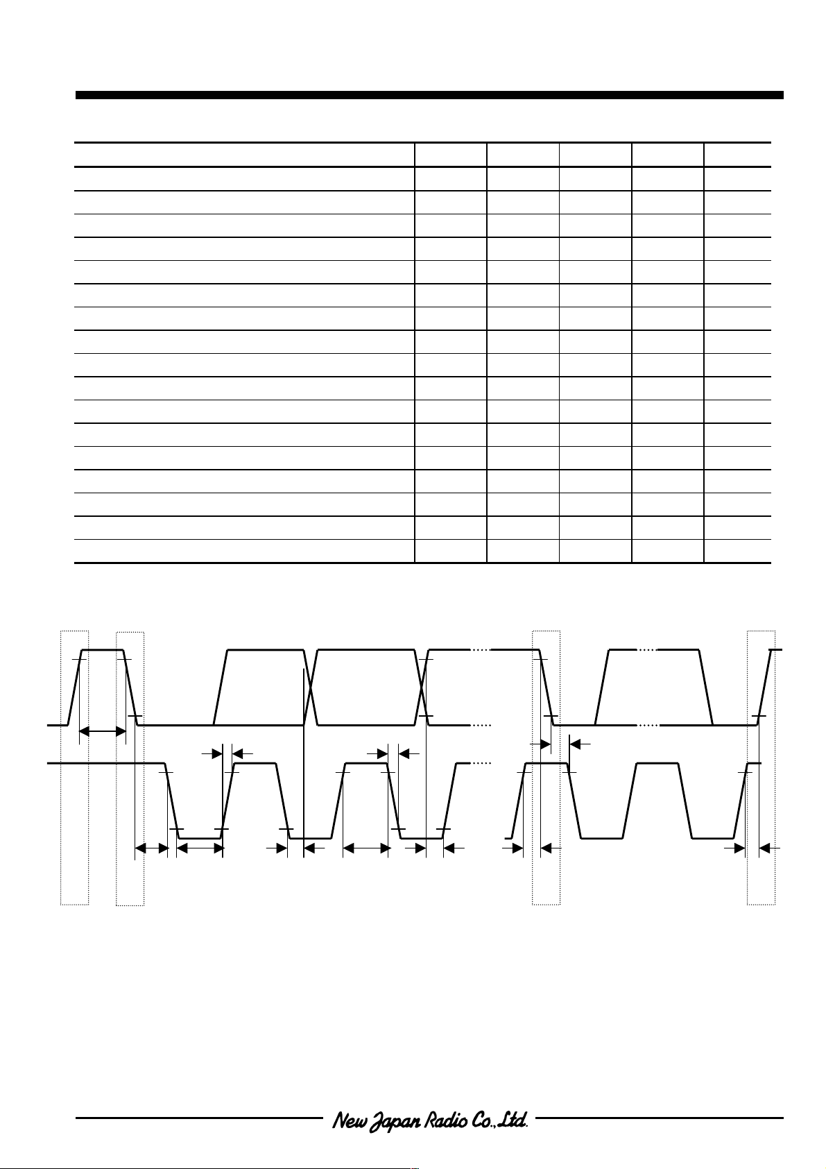
■■■■ I2C BUS BLOCK CHARACTERISTICS (SDA,SCL)
PARAMETER SYMBOL MIN. TYP. MAX. UNIT
High Level Input Voltage VIH 3.0 - 5.0 V
Low Level Input Voltage VIL 0 - 1.5 V
High Level Input Current IIH - - 10 µA
Low Level Input Current IIL - - 10 µA
Low Level Output Voltage (3mA at SDA pin) VOL 0 - 0.4 V
Maximum Output Current IOL -3.0 - - mA
Maximum Clock Frequency f
Data Change Minimum Waiting Time t
Data Transfer Start Minimum Waiting Time t
Low Level Clock Pulse Width t
High Level Clock Pulse Width T
Minimum Start Preparation Waiting Time t
Minimum Data Hold Time t
Minimum Data Preparation Time t
0 - 100 kHz
SCL
4.7 - - µs
BUF
4.0 - - µs
HD:STA
4.7 - - µs
LOW
4.0 - - µs
HIGH
4.7 - - µs
SU:STA
5.0 - - µs
HD:DAT
250 - - ns
SU:DAT
Rise Time tR - - 1.0 µs
Fall Time tF - - 300 ns
Minimum Stop Preparation Waiting Time t
2
C BUS Load Condition: Pull up resistance 4kΩ (Connected to +5V)
I
4.7 - - µs
SU:STO
Load capacitance 200pF (Connected to GND)
SDA
SCL
t
LOW
tR
t
HD:DA
t
BU
t
HD:ST
t
HIGH
tF
t
HD:ST
t
t
SU:DA
SU:ST
t
SU:ST
Sr
NJW1136
(
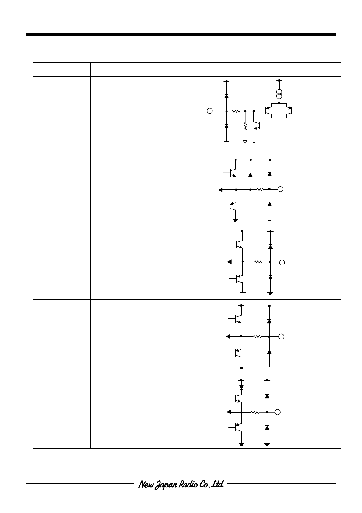
TERMINAL DESCRIPTION
No. SYMBOL FUNCTION EQUIVALENT CIRCUIT VOLTAGE
V+
1
32
6
7
26
INa
INb
OUTw
OUTa
OUTb
Ach input terminal
Bch input terminal
Subwoofer output terminal
Ach output terminal
Bch output terminal
2 SRFIL Surround filter terminal
1,32 pin
FB
FB
20k
80k
Vref
100
1.8k
V+/2
6, 7, 26pin
V+/2
2pin
V+/2
3 SSFIL Simulated stereo filter terminal
4
28
TONE-Ha
TONE-Hb
Treble(tone control) filter terminal
FB
FB
5.3k
18k
3pin
V+/2
4, 28pin
V+/2
6/24)
(7/24)
NJW1136
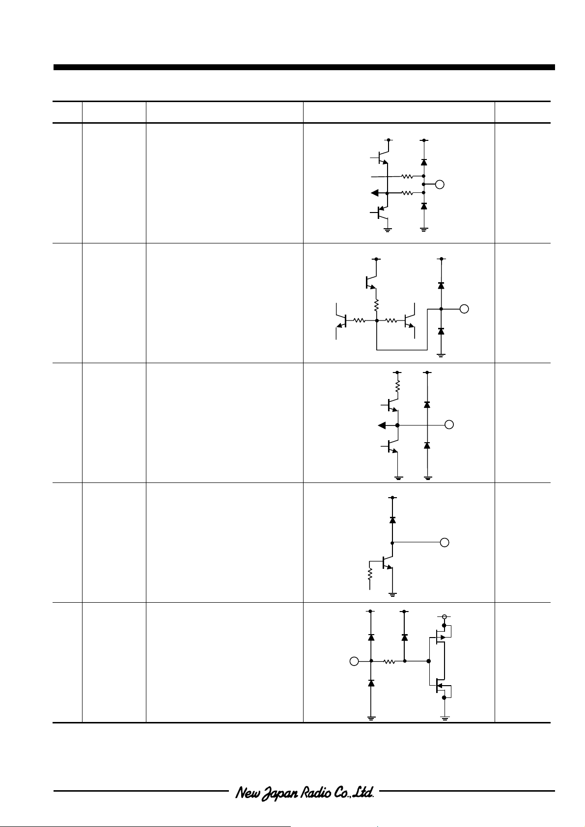
TERMINAL DESCRIPTION
No. SYMBOL FUNCTION EQUIVALENT CIRCUIT VOLTAGE
5
TONE-La
27
TONE-Lb
8 AGC1
9 AUX0
Bass(tone control) filter terminal
Capacitor connection terminal for
AGC attack and recovery time setting
Auxiliary 3 values voltage output terminal
12k
FB
400
12k
12k
1.4V
400
5, 27pin
V+/2
8pin
1k
9pin
FB
0V, 2.5V,
5.0V
10 AUX1
11
12
13
PORT0
PORT1
ADR
Auxiliary 2 values voltage output terminal
(Open collector type output)
Logic input terminal
Logic input terminal
Slave address setting terminal
(Don’t apply over 5V to these terminals)
12k
11, 12, 13pin
10pin
0V
3.5 to V+
5V
560
-
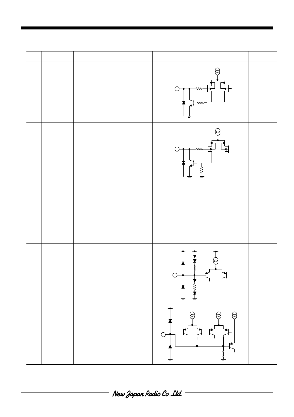
NJW1136
(
TERMINAL DESCRIPTION
No. SYMBOL FUNCTION EQUIVALENT CIRCUIT VOLTAGE
14 SDA I2C data terminal
15 SCL I2C clock terminal
16
17
GND
V+
Ground terminal
Supply voltage terminal
15pin
14pin
4k
-
8k
4k
-
8k
- V+/2
18 Vref Reference voltage terminal
19 CSR
DAC output for surround control terminal
18pin
19pin
200k
V+/2
200k
0V
32k
8/24)

(9/24)
TERMINAL DESCRIPTION
NJW1136
No. SYMBOL FUNCTION EQUIVALENT CIRCUIT VOLTAGE
20
21
22
23
24
CTL
CTH
CVW
CVB
CVA
25 AGC2
DAC output for tone control terminal
DAC output terminal for trimmer control
DAC output terminal for Bch volume control
DAC output terminal for Ach volume control
Resistance connection terminal for AGC
boost level setting
20, 21pin
22, 23,
24pin
25pin
36k
V+/2
V+/2
0V
29
30
LF3
LF2
LPF filter terminal
31 LF1 LPF filter terminal
29, 30pin
V+/2+0.7V
24k 4k
FB
V+/2

NJW1136
(
■■■■ MEASUREMENT CIRCUIT
Input Ach Input Bch
Output Wc h
Outp ut A ch
47k
AUX0
AUX1
(✳1)
PO R T0
PO R T1
ADR
SDA
SCL
V
PTIN0
V
PTIN1
V
ADRIN
(✳3)
47k
(✳2)
0.47µ
100n
100n
2.2n
100n
4.7µ
4.7µ
330nF
1
2
3
4
5
6
7
8
9
10
11
12
13
14
15
16
INa
SR-FIL
SS-FIL
TONE-Ha
TONE-La
OUTw
OUTa
AGC1
AUX0
AUX1
PORT0
PORT1
ADR
SDA
SCL
GND
INb
LF1
LF2
LF3
TONE-Hb
TONE-Lb
OUTb
AGC2
CVA
CVB
CVW
CTH
CTL
CSR
Vref
V+
32
31
30
29
28
27
26
25
24
23
22
21
20
19
18
17
0.47µ
0.033µ
0.047µ
0.022µ
2.2n
100n
4.7µ
100k
4.7µ
4.7µ
4.7µ
4.7µ
4.7µ
4.7µ
4.7µ
22µ
Vin Vin
Output Bch
Ic c
V+
47k
Vref
V+
(✳1)
I
V
AUX0
AUX0
Output High +2mA
Output Low -120µA
(✳2)
I
V
AUX1
AUX1
Output Low -3mA
(✳3)
I
V
OL
OL
Output Low -3mA
10/24)

(11/24)
A
A
f
■■■■ APPLICATION CIRCUIT
NJW1136
5V
100n
100n
2.2n
100n
4.7µ
4.7µ
330nF
4.7k
0.47µ
220
220
1
2
3
4
5
6
7
8
9
10
11
12
INa
SR-FIL
SS-FIL
TONE-Ha
TONE-La
OUTw
OUTa
AGC1
AUX0
AUX1
PORT0
PORT1
INb
LF1
LF2
LF3
TONE-Hb
TONE-Lb
OUTb
GC2
CV
CVB
CVW
CTH
32
31
30
29
28
27
26
25
24
23
22
21
0.47µ
0.033µ
0.047µ
0.022µ
2.2n
100n
4.7µ
100k
4.7µ
4.7µ
4.7µ
4.7µ
(✳4)
13
100
14
220
15
16
(✳4) Set the Slave Address by “ADR” terminal.
ADR pin (13pin) “ADR” bit
GND 0
+5V 1
ADR
SDA
SCL
GND
CTL
CSR
Vre
V+
20
19
18
17
4.7µ
4.7µ
4.7µ
22µ

NJW1136
(
C
G
■■■■ LPF Characteristics
R=24k
+
gm1
-
gm2
+
-
+
-
Primary LPF Secondary LPF
LF1 LF2 LF3
C1 C2 C3
LPF Block Diagram
The NJW1136 includes the LPF for subwoofer output and bass boost function. The LPF consists of primary and
secondary LPF and it is enable to adjust “cut off frequency”, “Q” and “Roll off”.
The expression of LPF characteristics is as follows.
<Primary LPF>
f
c
1
1
==
1**2
CR
π
<Secondary LPF>
6
−
109.42
f
=
c
2
∗
322
CC
∗
π
<LPF Frequency Response>
C2 = 47nF, C3 = 22nF
5
0
C1=33nF
C1=22nF
-5
C1=15nF
-10
Gain[dB]
-15
-20
0.1
1
Frequency [kHz]
π
C1=68nF
C1=47nF
1
Q =
2
−
3
1*10*24*2
C
3
C
*46.1
2
C
5
0
C2=47nF
-5
C2=68nF
C2=100nF
-10
-15
-20
5.01=Q
C1 = 33nF, C
C2=33nF
0.1 1
Fr
-10
Gain[dB]
-15
-20
5
0
C3=22nF
C3=15nF
-5
C1 = 33nF, C2 = 47nF
C3=47nF
C3=33nF
C3=10nF
0.1 1
Frequency [kHz]
12/24)

(13/24)
■■■■ DEFINITION OF I2C REGISTER
2
♦♦♦♦I
C BUS FORMAT
MSB LSB MSB LSB MSB LSB
NJW1136
S Slave Address A Select Address A Data A P
1bit 8bit 1bit 8bit 1bit 8bit 1bit 1bit
S: Starting Term
A: Acknowledge Bit
P: Ending Term
♦♦♦♦SLAVE ADDRESS
R/W : Set the Write Mode or Read Mode.
ADR : Set the Slave Address by “ADR” terminal. (See Application Circuit)
Slave Address Hex
MSB LSB -
1 0 0 0 0 0 ADR R/W
◆◆◆◆ R/W = 0 : Write Mode, ADR = 0/1 -
1 0 0 0 0 0 0 0 80(h)
1 0 0 0 0 0 1 0 82(h)
◆◆◆◆ R/W = 1 : Read Mode, ADR = 0/1 -
1 0 0 0 0 0 0 1 81(h)
1 0 0 0 0 0 1 1 83(h)
-
♦♦♦♦CONTROL REGISTER TABLE
The select address sets each function (Volume, Balance, Bass Boost Select, AGC, Surround, Tone Control, AUX).
The auto increment function cycles the select address as follows.
00H→01H→02H→03H→04H→05H→00H
<Write Mode>
Select
Address
00H
01H
02H TRIM
03H BCB BASS
04H BCT TREB
05H SUR AUX1 AUX0 AGCL AGC
<Read Mode>
D7 D6 D5
D7 D6 D5
CHS BAL BBSW
✴ : Don’t Care
1 1 1 1 1 1
•PORT1, PORT0 terminal setting
D1/D0 Remarks
0 D1/D0 output “0” at PORT1/PORT0 terminal receive High signal “1” (more than 3.5V)
1 D1/D0 output “1” at PORT1/PORT0 terminal receive Low signal “0” (less than 1.0V)
BIT
D4 D3 D2 D1 D0
VOL
✴
✴
✴
BIT
D4 D3 D2 D1 D0
PORT1 PORT0
♦♦♦♦CONTROL REGISTER DEFAULT VALUE
Control register default value is all “0”.
Select
Address
00H
01H
02H 0 0 0 0 0 0 0 0
03H 0 0 0 0 0 0 0 0
04H 0 0 0 0 0 0 0 0
05H 0 0 0 0 0 0 0 0
D7 D6 D5
0 0 0 0 0 0 0 0
0 0 0 0 0 0 0 0
BIT
D4 D3 D2 D1 D0

NJW1136
(
INSTRUCTION CODE
a) MASTER VOLUME SETTING
Select
Address
00H
•VOL Attenuation level : 0 to –80dB(0.33dB/step) , MUTE
The attenuator is consisted of both the VOL1(0.165dB/step)and VOL2(0.165dB/step) and is enable to adjust 0.33dB/step.
The attenuation for both the VOL1and VOL2 are always synchronized to have the same attenuation levels for each other,
and are not controllable independently for each other.
ex) VOL(-30dB) = VOL1(-15dB) + VOL2(-15dB)
D7 D6 D5
BIT
D4 D3 D2 D1 D0
VOL
b) BALANCE AND BASS BOOST FUNCTION SETTING
Select
Address
01H
•CHS : Channel select for balance control
“0” : Ach “Bch is attenuated”
“1” : Bch “Ach is attenuated”
•BAL : Balance control for both Ach and Bch
Balance Level : 0 to –60dB (1dB/Step) , MUTE
•BBSW : Bass Boost ON/OFF Switch
“0” = Bass Boost OFF
“1” = Bass Boost ON
D7 D6 D5
CHS BAL BBSW
BIT
D4 D3 D2 D1 D0
c) TRIMMER LEVEL SETTING
Select
Address
02H
•TRIM : Trimmer Level
Trimmer Level : +18 to –44dB (0.5dB/Step) , MUTE
D7 D6 D5
BIT
D4 D3 D2 D1 D0
TRIM
Don’t Care
d) TONE CONTROL BASS SETTING
Select
Address
03H
•BCB : Boost cut select for Bass control
“0” : Cut
“1” : Boost
•BASS : BASS Level Setting
Cut Level : -15 to 0dB(0.5dB/Step)
Boost Level : 0 to +15dB(0.5dB/Step)
D7 D6 D5
BCB BASS
BIT
D4 D3 D2 D1 D0
Don’t Care
d) TONE CONTROL TREBLE SETTING
Select
Address
04H
•BCT : Boost cut select for Treble control
“0” : Cut
“1” : Boost
•TREB : TREBLE Level Setting
Cut Level : -15 to 0dB(0.5dB/Step)
Boost Level : 0 to +15dB(0.5dB/Step)
D7 D6 D5
BCT TREB
BIT
D4 D3 D2 D1 D0
Don’t Care
14/24)

(15/24)
d) SURROUND, AUXILIARY, AGC LEVEL SETTING
Select
Address
05H
D7 D6 D5
SUR AUX1 AUX0
<SUR : Surround Level Setting>
Surround Setting D7 D6 Remarks
Surround Off 0 0 Surround Off
Simulated Stereo 0 1 Simulated Stereo
Surround Effect1 1 0 Surround Effect Low(8.3dB typ.)
Surround Effect2 1 1 Surround Effect High(12.7dB typ.)
<AUX1 : AUX1 Terminal Setting>
Auxiliary Setting D5
Low (0.0V) 0
High (5.0V) 1
<AUX0 : AUX0 Terminal Setting>
Auxiliary Setting D4 D3
Low (0.0V) - 0
Mid (2.5V) 0 1
High (5.0V) 1 1
<AGCL : AGC Level Setting>
AGC Level Setting D2 D1
100mVrms 0 0
200mVrms 0 1
300mVrms 1 0
400mVrms 1 1
<AGC : AGC Setting>
AGC Setting D0
OFF 0
ON 1
BIT
D4 D3 D2 D1 D0
AGCL AGC
NJW1136

NJW1136
(
■■■■Master Volume (Select Address : 00H)
Gain(dB) HEX D7 D6 D5 D4 D3 D2 D1 D0
0 FF 1 1 1 1 1 1 1 1
-1 FC 1 1 1 1 1 1 0 0
-2 F9 1 1 1 1 1 0 0 1
-3 F6 1 1 1 1 0 1 1 0
-4 F3 1 1 1 1 0 0 1 1
-5 F0 1 1 1 1 0 0 0 0
-6 ED 1 1 1 0 1 1 0 1
-7 EA 1 1 1 0 1 0 1 0
-8 E7 1 1 1 0 0 1 1 1
-9 E4 1 1 1 0 0 1 0 0
-10 E1 1 1 1 0 0 0 0 1
-11 DE 1 1 0 1 1 1 1 0
-12 DB 1 1 0 1 1 0 1 1
-13 D8 1 1 0 1 1 0 0 0
-14 D5 1 1 0 1 0 1 0 1
-15 D2 1 1 0 1 0 0 1 0
-16 CF 1 1 0 0 1 1 1 1
-17 CC 1 1 0 0 1 1 0 0
-18 C9 1 1 0 0 1 0 0 1
-19 C6 1 1 0 0 0 1 1 0
-20 C3 1 1 0 0 0 0 1 1
-21 C0 1 1 0 0 0 0 0 0
-22 BD 1 0 1 1 1 1 0 1
-23 BA 1 0 1 1 1 0 1 0
-24 B7 1 0 1 1 0 1 1 1
-25 B4 1 0 1 1 0 1 0 0
-26 B1 1 0 1 1 0 0 0 1
-27 AE 1 0 1 0 1 1 1 0
-28 AB 1 0 1 0 1 0 1 1
-29 A8 1 0 1 0 1 0 0 0
-30 A5 1 0 1 0 0 1 0 1
-31 A2 1 0 1 0 0 0 1 0
-32 9F 1 0 0 1 1 1 1 1
-33 9C 1 0 0 1 1 1 0 0
-34 99 1 0 0 1 1 0 0 1
-35 96 1 0 0 1 0 1 1 0
-36 93 1 0 0 1 0 0 1 1
-37 90 1 0 0 1 0 0 0 0
-38 8D 1 0 0 0 1 1 0 1
-39 8A 1 0 0 0 1 0 1 0
-40 87 1 0 0 0 0 1 1 1
-41 84 1 0 0 0 0 1 0 0
-42 81 1 0 0 0 0 0 0 1
VOL
16/24)

(17/24)
NJW1136
Gain(dB) HEX D7 D6 D5 D4 D3 D2 D1 D0
-43 7E 0 1 1 1 1 1 1 0
-44 7B 0 1 1 1 1 0 1 1
-45 78 0 1 1 1 1 0 0 0
-46 75 0 1 1 1 0 1 0 1
-47 72 0 1 1 1 0 0 1 0
-48 6F 0 1 1 0 1 1 1 1
-49 6C 0 1 1 0 1 1 0 0
-50 69 0 1 1 0 1 0 0 1
-51 66 0 1 1 0 0 1 1 0
-52 63 0 1 1 0 0 0 1 1
-53 60 0 1 1 0 0 0 0 0
-54 5D 0 1 0 1 1 1 0 1
-55 5A 0 1 0 1 1 0 1 0
-56 57 0 1 0 1 0 1 1 1
-57 54 0 1 0 1 0 1 0 0
-58 51 0 1 0 1 0 0 0 1
-59 4E 0 1 0 0 1 1 1 0
-60 4B 0 1 0 0 1 0 1 1
-61 48 0 1 0 0 1 0 0 0
-62 45 0 1 0 0 0 1 0 1
-63 42 0 1 0 0 0 0 1 0
-64 3F 0 0 1 1 1 1 1 1
-65 3C 0 0 1 1 1 1 0 0
-66 39 0 0 1 1 1 0 0 1
-67 36 0 0 1 1 0 1 1 0
-68 33 0 0 1 1 0 0 1 1
-69 30 0 0 1 1 0 0 0 0
-70 2D 0 0 1 0 1 1 0 1
-71 2A 0 0 1 0 1 0 1 0
-72 27 0 0 1 0 0 1 1 1
-73 24 0 0 1 0 0 1 0 0
-74 21 0 0 1 0 0 0 0 1
-75 1E 0 0 0 1 1 1 1 0
-76 1B 0 0 0 1 1 0 1 1
-77 18 0 0 0 1 1 0 0 0
-78 15 0 0 0 1 0 1 0 1
-79 12 0 0 0 1 0 0 1 0
-80 0F 0 0 0 0 1 1 1 1
MUTE✴ 00 0 0 0 0 0 0 0 0
VOL
✴ : Default Value

NJW1136
(
■■■■Balance, Bass Boost Setting (Select Address : 01H)
Channel Setting (CHS) D7
Decrease Bch Gain 0
Decrease Ach Gain 1
Gain(dB)
0✴ 0 0 0 0 0 0
-1
-2
-3
-4
-5
-6
-7
-8
-9
-10
-11
-12
-13
-14
-15
-16
-17
-18
-19
-20
-21
-22
-23
-24
-25
-26
-27
-28
-29
-30
✴ : Default Value
D6 D5 D4 D3 D2 D1
0
0
0
0
0
0
0
0
0
0
0
0
0
0
0
0
0
0
0
0
0
0
0
0
0
0
0
0
0
0
0 0 0 0 1
0 0 0 1 0
0 0 0 1 1
0 0 1 0 0
0 0 1 0 1
0 0 1 1 0
0 0 1 1 1
0 1 0 0 0
0 1 0 0 1
0 1 0 1 0
0 1 0 1 1
0 1 1 0 0
0 1 1 0 1
0 1 1 1 0
0 1 1 1 1
1 0 0 0 0
1 0 0 0 1
1 0 0 1 0
1 0 0 1 1
1 0 1 0 0
1 0 1 0 1
1 0 1 1 0
1 0 1 1 1
1 1 0 0 0
1 1 0 0 1
1 1 0 1 0
1 1 0 1 1
1 1 1 0 0
1 1 1 0 1
1 1 1 1 0
BAL
18/24)

(19/24)
NJW1136
Gain(dB)
-31
-32 1 0 0 0 0 0
-33
-34
-35
-36
-37
-38
-39
-40
-41
-42
-43
-44
-45
-46
-47
-48
-49
-50
-51
-52
-53
-54
-55
-56
-57
-58
-59
-60
MUTE
Bass Boost Setting (BBSW) D0
Bass Boost Off✴ 0
Bass Boost On 1
D6 D5 D4 D3 D2 D1
0
1
1
1
1
1
1
1
1
1
1
1
1
1
1
1
1
1
1
1
1
1
1
1
1
1
1
1
1
1
✴ : Default Value
1 1 1 1 1
0 0 0 0 1
0 0 0 1 0
0 0 0 1 1
0 0 1 0 0
0 0 1 0 1
0 0 1 1 0
0 0 1 1 1
0 1 0 0 0
0 1 0 0 1
0 1 0 1 0
0 1 0 1 1
0 1 1 0 0
0 1 1 0 1
0 1 1 1 0
0 1 1 1 1
1 0 0 0 0
1 0 0 0 1
1 0 0 1 0
1 0 0 1 1
1 0 1 0 0
1 0 1 0 1
1 0 1 1 0
1 0 1 1 1
1 1 0 0 0
1 1 0 0 1
1 1 0 1 0
1 1 0 1 1
1 1 1 0 0
1 1 1 1 1
BAL

NJW1136
(
■■■■Trimmer Setting (Select Address: 02H)
Gain(dB) D7 D6 D5 D4 D3 D2 D1
TRIM
+18.0
+17.5
+17.0
+16.5
+16.0
+15.5
+15.0
+14.5
+14.0
+13.5
+13.0 1 1 1 0 1 0 1
+12.5
+12.0
+11.5
+11.0
+10.5 1 1 1 0 0 0 0
+10.0
+9.5
+9.0
+8.5
+8.0
+7.5
+7.0
+6.5
+6.0
+5.5
+5.0
+4.5
+4.0
+3.5
+3.0
+2.5
+2.0
+1.5
+1.0
+0.5
0.0
-0.5
-1.0
-1.5
-2.0
-2.5
-3.0
-3.5
-4.0
-4.5
-5.0
-5.5
-6.0
1 1 1 1 1 1 1
1 1 1 1 1 1 0
1 1 1 1 1 0 1
1 1 1 1 1 0 0
1 1 1 1 0 1 1
1 1 1 1 0 1 0
1 1 1 1 0 0 1
1 1 1 1 0 0 0
1 1 1 0 1 1 1
1 1 1 0 1 1 0
1 1 1 0 1 0 0
1 1 1 0 0 1 1
1 1 1 0 0 1 0
1 1 1 0 0 0 1
1 1 0 1 1 1 1
1 1 0 1 1 1 0
1 1 0 1 1 0 1
1 1 0 1 1 0 0
1 1 0 1 0 1 1
1 1 0 1 0 1 0
1 1 0 1 0 0 1
1 1 0 1 0 0 0
1 1 0 0 1 1 1
1 1 0 0 1 1 0
1 1 0 0 1 0 1
1 1 0 0 1 0 0
1 1 0 0 0 1 1
1 1 0 0 0 1 0
1 1 0 0 0 0 1
1 1 0 0 0 0 0
1 0 1 1 1 1 1
1 0 1 1 1 1 0
1 0 1 1 1 0 1
1 0 1 1 1 0 0
1 0 1 1 0 1 1
1 0 1 1 0 1 0
1 0 1 1 0 0 1
1 0 1 1 0 0 0
1 0 1 0 1 1 1
1 0 1 0 1 1 0
1 0 1 0 1 0 1
1 0 1 0 1 0 0
1 0 1 0 0 1 1
1 0 1 0 0 1 0
1 0 1 0 0 0 1
1 0 1 0 0 0 0
1 0 0 1 1 1 1
20/24)

(21/24)
NJW1136
Gain(dB) D7 D6 D5 D4 D3 D2 D1
-6.5
-7.0
-7.5
-8.0
-8.5
-9.0
-9.5
-10.0
-10.5
-11.0
-11.5
-12.0 1 0 0 0 0 1 1
-12.5
-13.0
-13.5
-14.0
-14.5
-15.0
-15.5
-16.0
-16.5
-17.0
-17.5
-18.0
-18.5
-19.0
-19.5
-20.0
-20.5
-21.0
-21.5
-22.0
-22.5
-23.0
-23.5
-24.0
-24.5
-25.0
-25.5
-26.0
-26.5
-27.0
-27.5
-28.0
-28.5
-29.0
-29.5
-30.0
-30.5
-31.0
1 0 0 1 1 1 0
1 0 0 1 1 0 1
1 0 0 1 1 0 0
1 0 0 1 0 1 1
1 0 0 1 0 1 0
1 0 0 1 0 0 1
1 0 0 1 0 0 0
1 0 0 0 1 1 1
1 0 0 0 1 1 0
1 0 0 0 1 0 1
1 0 0 0 1 0 0
1 0 0 0 0 1 0
1 0 0 0 0 0 1
1 0 0 0 0 0 0
0 1 1 1 1 1 1
0 1 1 1 1 1 0
0 1 1 1 1 0 1
0 1 1 1 1 0 0
0 1 1 1 0 1 1
0 1 1 1 0 1 0
0 1 1 1 0 0 1
0 1 1 1 0 0 0
0 1 1 0 1 1 1
0 1 1 0 1 1 0
0 1 1 0 1 0 1
0 1 1 0 1 0 0
0 1 1 0 0 1 1
0 1 1 0 0 1 0
0 1 1 0 0 0 1
0 1 1 0 0 0 0
0 1 0 1 1 1 1
0 1 0 1 1 1 0
0 1 0 1 1 0 1
0 1 0 1 1 0 0
0 1 0 1 0 1 1
0 1 0 1 0 1 0
0 1 0 1 0 0 1
0 1 0 1 0 0 0
0 1 0 0 1 1 1
0 1 0 0 1 1 0
0 1 0 0 1 0 1
0 1 0 0 1 0 0
0 1 0 0 0 1 1
0 1 0 0 0 1 0
0 1 0 0 0 0 1
0 1 0 0 0 0 0
0 0 1 1 1 1 1
0 0 1 1 1 1 0
0 0 1 1 1 0 1
TRIM

NJW1136
(
Gain(d
(dB))))
(d(d
-31.5
-32.0
-32.5
-33.0
-33.5
-34.0
-34.5
-35.0
-35.5
-36.0
-36.5
-37.0 0 0 1 0 0 0 1
-37.5
-38.0
-38.5
-39.0
-39.5
-40.0
-40.5
-41.0
-41.5
-42.0
-42.5
-43.0
-43.5
-44.0
MUTE✴
✴ : Default value
D7 D6 D5 D4 D3 D2 D1
0 0 1 1 1 0 0
0 0 1 1 0 1 1
0 0 1 1 0 1 0
0 0 1 1 0 0 1
0 0 1 1 0 0 0
0 0 1 0 1 1 1
0 0 1 0 1 1 0
0 0 1 0 1 0 1
0 0 1 0 1 0 0
0 0 1 0 0 1 1
0 0 1 0 0 1 0
0 0 1 0 0 0 0
0 0 0 1 1 1 1
0 0 0 1 1 1 0
0 0 0 1 1 0 1
0 0 0 1 1 0 0
0 0 0 1 0 1 1
0 0 0 1 0 1 0
0 0 0 1 0 0 1
0 0 0 1 0 0 0
0 0 0 0 1 1 1
0 0 0 0 1 1 0
0 0 0 0 1 0 1
0 0 0 0 1 0 0
0 0 0 0 0 1 1
0 0 0 0 0 0 0
TRIM
22/24)

(23/24)
NJW1136
■■■■Tone Control(Bass Setting) (Select Address : 03H)
Bass
Cut or Boost
Cut 0
Boost 1
BASS
Cut Gain(dB) Boost Gain(dB) D6 D5 D4 D3 D2
-15.0 15.0 1 1 1 1 0
-14.5 14.5 1 1 1 0 1
-14.0 14.0 1 1 1
-13.5 13.5 1 1 0 1 1
-13.0 13.0 1 1 0 1 0
-12.5 12.5 1 1 0 0 1
-12.0 12.0 1 1 0
-11.5 11.5 1 0 1 1 1
-11.0 11.0 1 0 1 1 0
-10.5 10.5 1 0 1 0 1
-10.0 10.0 1 0 1
-9.5 9.5 1 0 0 1 1
-9.0 9.0 1 0 0 1 0
-8.5 8.5 1 0 0 0 1
-8.0 8.0 1 0 0
-7.5 7.5 0 1 1 1 1
-7.0 7.0 0 1 1 1 0
-6.5 6.5 0 1 1 0 1
-6.0 6.0 0 1 1
-5.5 5.5 0 1 0 1 1
-5.0 5.0 0 1 0 1 0
-4.5 4.5 0 1 0 0 1
-4.0 4.0 0 1 0
-3.5 3.5 0 0 1 1 1
-3.0 3.0 0 0 1 1 0
-2.5 2.5 0 0 1 0 1
-2.0 2.0 0 0 1
-1.5 1.5 0 0 0 1 1
-1.0 1.0 0 0 0 1 0
-0.5 0.5 0 0 0 0 1
0.0✴ 0.0✴
✴ : Default value
BCB
D7
0 0
0 0
0 0
0 0
0 0
0 0
0 0
0 0 0 0 0

NJW1136
(
■■■■Tone Control(Treble Setting) (Select Address : 04H)
Trebl e
Cut or Boost
BCT
D7
Cut 0
Boost 1
TREB
Cut Gain(dB) Boost Gain(dB) D6 D5 D4 D3 D2
-15.0 15.0 1 1 1 1 0
-14.5 14.5 1 1 1 0 1
-14.0 14.0 1 1 1
0 0
-13.5 13.5 1 1 0 1 1
-13.0 13.0 1 1 0 1 0
-12.5 12.5 1 1 0 0 1
-12.0 12.0 1 1 0
0 0
-11.5 11.5 1 0 1 1 1
-11.0 11.0 1 0 1 1 0
-10.5 10.5 1 0 1 0 1
-10.0 10.0 1 0 1
0 0
-9.5 9.5 1 0 0 1 1
-9.0 9.0 1 0 0 1 0
-8.5 8.5 1 0 0 0 1
-8.0 8.0 1 0 0
0 0
-7.5 7.5 0 1 1 1 1
-7.0 7.0 0 1 1 1 0
-6.5 6.5 0 1 1 0 1
-6.0 6.0 0 1 1
0 0
-5.5 5.5 0 1 0 1 1
-5.0 5.0 0 1 0 1 0
-4.5 4.5 0 1 0 0 1
-4.0 4.0 0 1 0
0 0
-3.5 3.5 0 0 1 1 1
-3.0 3.0 0 0 1 1 0
-2.5 2.5 0 0 1 0 1
-2.0 2.0 0 0 1
0 0
-1.5 1.5 0 0 0 1 1
-1.0 1.0 0 0 0 1 0
-0.5 0.5 0 0 0 0 1
0.0✴ 0.0✴
0 0 0 0 0
✴ : Default value
■■■■NOTE
Purchase of I
conveys a license under the Philips I
the system conforms to the I
2
C components of New Japan Radio Co., Ltd or one of its sublicensed Associated Companies
2
C Standard Specification as defined by Philips.
2
C Patent Rights to use these components in an I2C system, provided that
[CAUTION]
The specifications on this databook are only
given for information , without any guarantee
as regards either mistakes or omissions. The
application circuits in this databook are
described only to show representative usages
of the product and not intended for the
guarantee or permission of any right including
the industrial rights.
24/24)
 Loading...