

Page 1
NJU6676
64-common X 132-segment + 1-icon common
Bit Map LCD Driver
■
GENERAL DESCRIPTION ■ PACKAGE
NJU6676
The
graphics or characters. It contains 8,580 bits display
data RAM, microprocessor interface circuits,
instruction decoder, 132-segment drivers, 64-common
drivers and 1-icon common driver.
The bit image display data is transferred to the
display data RAM by serial or 8-bit parallel interface.
65 x 132 dots graphics or 8-character 4-line by 16 x
16 dots character with icon are displayed by
itself.
The wide operating voltage from 2.2 to 5.5V and low
operating current are useful for small size battery
operating items.
The build-in Electrical Variable Resistance is very
precision, furthermore the rectangle outlook is very
applicable to COG or Slim TCP.
■
FEATURES
● Direct Correspondence between Display Data RAM and LCD Pixel
● Display Data RAM - 8,580 bits
● 197 LCD Drivers - 64-common and 132-segment + 1-icon common
● Direct Microprocessor Interface for both of 68 and 80 type MPU
● Serial Interface
● Programmable Bias selection ; 1/7,1/9 bias
● Useful Instruction Set
Display ON/OFF Cont, Display Sta rt Lin e Set , Pa ge Address Set, Column Address Set, Status Read,
Display Data Read/Write, ADC Select, Inverse Display, All On/Off, Bias Select, Read Modify Write,
End, Reset, Common Driver order Assignment, Power control set, Driver On/Off, EVR Mode Set,
EVR Registe r S et, Static Ind icator On/Off, Static In dicator Regist er Set, Power Saving.
● Power Supply Circuits for LCD Incorporated
Vol tage Booster Circuits (4-time Maximum), Regulator, Volt age Follower x 4
● Precision Electrical Variable Resistance (64-step)
● Low Power Consumption 80uA(Typ.).
● Operating Voltage (All the voltages are based on VDD=0V.)
- Logic Operating V oltage : -2.2V ∼ -5.5V
- Voltage Booster Operating Voltage : -2.5V ∼
- LCD Driving Voltage : -6.0V ∼ -18.0V
● Rectangle outlook for COG
● Package Outline : Bump-chip
● C-MOS Technology (Substrate : N)
is a bit map LCD driver to display
NJU6676
NJU6676CL
Ver.2004-03-01
-1-
Page 2

X
NJU6676
■
PAD LOCATION
DUMMY1
OSC1
OSC2
FRS
FR
CL
DOF
VSS
CS1
CS2
VDD
RES
A0
VSS
WR(R/W)
RD(E)
VDD
D0
D1
D2
D3
D4
D5
D6(SCL)
D7(SI)
VDD
VDD
VDD
VDD
VSS
VSS
VSS
VSS2
VSS2
VSS2
VSS2
VOUT
VOUT
C3C3C1+
C1+
C1C1C2C2C2+
C2+
VSS
VSS
VDD
VDD
V1
V1
V2
V2
V3
V3
V4
V4
V5
V5
VR
VR
VDD
VDD
VDD
M/S
CLS
VSS
C86
P/S
VDD
VSS
VDD
DUMMY2
COMM
C31
C63
C32
C33
DUMMY4
S131
S130
Y
Chip Center : X=0um, Y=0um
Chip Size
:X=8.72mm,Y=2.37mm
Chip Thickness : 675um ± 30um
Bump Size
: 45um x 83um
Bump Pitch : 60um(Min.)
Bump Height : 15um(Typ.)
Bump Material : Au
Voltage Boosting Polarity
: Negative Volt age (VDD common)
Substrate : N
S1
C30
COMM
C0
- 2 -
Ver.2004-03-01
Page 3
NJU6676
■
PAD COORDINATES
Chip Size 8.72 x 2.37mm(Chip Center X=0um, Y=0um)
P AD No. Terminal X(um) Y(um) P AD No. Terminal X(um) Y(um)
1 DUMMY1 -4139 -1025 51 VDD 1655 -1025
2 OSC1 -3347 -1025 52 VDD 1715 -1025
3 OSC2 -3287 -1025 53 V1 1775 -1025
4 FRS -3129 -1025 54 V1 1835 -1025
5 FR -2909 -1025 55 V2 1895 -1025
6 CL -2688 -1025 56 V2 1955 -1025
7 DOF -2468 -1025 57 V3 2015 -1025
8 VSS -2311 -1025 58 V3 2075 -1025
9 CS1 -2251 -1025 59 V4 2135 -1025
10 CS2 -2191 -1025 60 V4 2195 -1025
11 VDD -2131 -1025 61 V5 2255 -1025
12 RES -2071 -1025 62 V5 2315 -1025
13 A0 -2011 -1025 63 VR 2375 -1025
14 VSS -1951 -1025 64 VR 2435 -1025
15 WR -1891 -1025 65 VDD 2495 -1025
16 RD -1831 -1025 66 VDD 2555 -1025
17 VDD -1771 -1025 67 VDD 2615 -1025
18 D0 -1613 -1025 68 M/S 2675 -1025
19 D1 -1393 -1025 69 CLS 2810 -1025
20 D2 -1172 -1025 70 VSS 2870 -1025
21 D3 -952 -1025 71 C86 2930 -1025
22 D4 -731 -1025 72 P/S 3065 -1025
23 D5 -511 -1025 73 VDD 3125 -1025
24 D6(SCL) -291 -1025 74 VSS 3185 -1025
25 D7(SI) -70 -1025 75 VDD 3245 -1025
26 VDD 155 -1025 76 DUMMY2 4139 -1025
27 VDD 215 -1025 77 C31 4200 -935
28 VDD 275 -1025 78 C30 4200 -875
29 VDD 335 -1025 79 C29 4200 -815
30 VSS 395 -1025 80 C28 4200 -755
31 VSS 455 -1025 81 C27 4200 -695
32 VSS 515 -1025 82 C26 4200 -635
33 VSS2 575 -1025 83 C25 4200 -575
34 VSS2 635 -1025 84 C24 4200 -515
35 VSS2 695 -1025 85 C23 4200 -455
36 VSS2 755 -1025 86 C22 4200 -395
37 VOUT 815 -1025 87 C21 4200 -335
38 VOUT 875 -1025 88 C20 4200 -275
39 C3- 935 -1025 89 C19 4200 -215
40 C3- 995 -1025 90 C18 4200 -155
41 C1+ 1055 -1025 91 C17 4200 -95
42 C1+ 1115 -1025 92 C16 4200 -35
43 C1- 1175 -1025 93 C15 4200 25
44 C1- 1235 -1025 94 C14 4200 85
45 C2- 1295 -1025 95 C13 4200 145
46 C2- 1355 -1025 96 C12 4200 205
47 C2+ 1415 -1025 97 C11 4200 265
48 C2+ 1475 -1025 98 C10 4200 325
49 VSS 1535 -1025 99 C9 4200 385
50 VSS 1595 -1025 100 C8 4200 445
Ver.2004-03-01
-3-
Page 4

NJU6676
P AD No. Terminal X(um) Y(um) P AD No. Terminal X(um) Y(um)
101 C7 4200 505 151 S40 1533 1025
102 C6 4200 565 152 S41 1473 1025
103 C5 4200 625 153 S42 1413 1025
104 C4 4200 685 154 S43 1353 1025
105 C3 4200 745 155 S44 1293 1025
106 C2 4200 805 156 S45 1233 1025
107 C1 4200 865 157 S46 1173 1025
108 C0 4200 925 158 S47 1113 1025
109 COMM 4200 985 159 S48 1053 1025
110 DUMMY3 4119 1025 160 S49 993 1025
111 S0 3933 1025 161 S50 933 1025
112 S1 3873 1025 162 S51 873 1025
113 S2 3813 1025 163 S52 813 1025
114 S3 3753 1025 164 S53 753 1025
115 S4 3693 1025 165 S54 693 1025
116 S5 3633 1025 166 S55 633 1025
117 S6 3573 1025 167 S56 573 1025
118 S7 3513 1025 168 S57 513 1025
119 S8 3453 1025 169 S58 453 1025
120 S9 3393 1025 170 S59 393 1025
121 S10 3333 1025 171 S60 333 1025
122 S11 3273 1025 172 S61 273 1025
123 S12 3213 1025 173 S62 213 1025
124 S13 3153 1025 174 S63 153 1025
125 S14 3093 1025 175 S64 93 1025
126 S15 3033 1025 176 S65 33 1025
127 S16 2973 1025 177 S66 -27 1025
128 S17 2913 1025 178 S67 -87 1025
129 S18 2853 1025 179 S68 -147 1025
130 S19 2793 1025 180 S69 -207 1025
131 S20 2733 1025 181 S70 -267 1025
132 S21 2673 1025 182 S71 -327 1025
133 S22 2613 1025 183 S72 -387 1025
134 S23 2553 1025 184 S73 -447 1025
135 S24 2493 1025 185 S74 -507 1025
136 S25 2433 1025 186 S75 -567 1025
137 S26 2373 1025 187 S76 -627 1025
138 S27 2313 1025 188 S77 -687 1025
139 S28 2253 1025 189 S78 -747 1025
140 S29 2193 1025 190 S79 -807 1025
141 S30 2133 1025 191 S80 -867 1025
142 S31 2073 1025 192 S81 -927 1025
143 S32 2013 1025 193 S82 -987 1025
144 S33 1953 1025 194 S83 -1047 1025
145 S34 1893 1025 195 S84 -1107 1025
146 S35 1833 1025 196 S85 -1167 1025
147 S36 1773 1025 197 S86 -1227 1025
148 S37 1713 1025 198 S87 -1287 1025
149 S38 1653 1025 199 S88 -1347 1025
150 S39 1593 1025 200 S89 -1407 1025
- 4 -
Ver.2004-03-01
Page 5

NJU6676
P AD No. Terminal X(um) Y(um) P AD No. Terminal X(um) Y(um)
201 S90 -1467 1025 251 C39 -4200 565
202 S91 -1527 1025 252 C40 -4200 505
203 S92 -1587 1025 253 C41 -4200 445
204 S93 -1647 1025 254 C42 -4200 385
205 S94 -1707 1025 255 C43 -4200 325
206 S95 -1767 1025 256 C44 -4200 265
207 S96 -1827 1025 257 C45 -4200 205
208 S97 -1887 1025 258 C46 -4200 145
209 S98 -1947 1025 259 C47 -4200 85
210 S99 -2007 1025 260 C48 -4200 25
211 S100 -2067 1025 261 C49 -4200 -35
212 S101 -2127 1025 262 C50 -4200 -95
213 S102 -2187 1025 263 C51 -4200 -155
214 S103 -2247 1025 264 C52 -4200 -215
215 S104 -2307 1025 265 C53 -4200 -275
216 S105 -2367 1025 266 C54 -4200 -335
217 S106 -2427 1025 267 C55 -4200 -395
218 S107 -2487 1025 268 C56 -4200 -455
219 S108 -2547 1025 269 C57 -4200 -515
220 S109 -2607 1025 270 C58 -4200 -575
221 S110 -2667 1025 271 C59 -4200 -635
222 S111 -2727 1025 272 C60 -4200 -695
223 S112 -2787 1025 273 C61 -4200 -755
224 S113 -2847 1025 274 C62 -4200 -815
225 S114 -2907 1025 275 C63 -4200 -875
226 S115 -2967 1025 276 COMM -4200 -935
227 S116 -3027 1025
228 S117 -3087 1025
229 S118 -3147 1025
230 S119 -3207 1025
231 S120 -3267 1025
232 S121 -3327 1025
233 S122 -3387 1025
234 S123 -3447 1025
235 S124 -3507 1025
236 S125 -3567 1025
237 S126 -3627 1025
238 S127 -3687 1025
239 S128 -3747 1025
240 S129 -3807 1025
241 S130 -3867 1025
242 S131 -3927 1025
243 DUMMY4 -4119 1025
244 C32 -4200 985
245 C33 -4200 925
246 C34 -4200 865
247 C35 -4200 805
248 C36 -4200 745
249 C37 -4200 685
250 C38 -4200 625
Ver.2004-03-01
-5-
Page 6
NJU6676
■
BLOCK DIAGRAM
Vss
VDD
V1 to V5
C1+/C1C2+/C2-
Internal
Power
Circuits
VR
Vout
C3-
Vss2
Voltage
Followers
Voltage
Regulator
Voltage
Converter
Instruction
Decoder
C0 - - - - C31 C63 - - - - C32
Drivers
Shift
Register
Low Address Decoder
Common Direction
Page Address Register
Internal Bus Line
S0 - - - - - - - - - - - - - S131 COMM
Segment Drivers Common
Display Data Latch
Display Da ta RAM
65 X 132 = 8,580-bit
Column Address Decoder
Column Address Counter
Column Address Register
Multiplexer
Status Busy Flag Bus Holder
Common
Drivers
Shift
Register
Common
Timing
Line Counter
Line Address Decoder
Initial Display Line
Display
Timing
Oscillator
M/S
FR
FRS
CL
CLS
DOF
OSC1
OSC2
Reset MPU Interface
RES CS1 WRRD
CS2 A0 C86 D7
(SI)
D6
(SCL)
P/S
D5 to D0
- 6 -
Ver.2004-03-01
Page 7
NJU6676
t
TERMINAL DESCRIPTION
■
No. Symbol Description
1,76,
110,243
11,17
26∼29
51,52
65∼67
73,75
8,14,
30,31,
32,49,
50,70,74
33∼36 VSS2 Reference voltage for voltage booster
53,54
55,56
57,58
59,60
61,62
41,42
43,44
47,48
45,46
39,40 C3- Boosted capacitor connecting terminals used for voltage booster.
DUMMY1~
DUMMY4
VDD VDD=+3V
VSS VSS=0V
V1
V2
V3
V4
V5
C1+
C1-
C2+
C2-
Dummy Terminals.
These ar e op en t er m in al s el ec t r ic a ll y.
LCD Driving Voltage Supplying Terminal. W hen the internal voltage booster
is not used, supply each level of LCD driving voltage from outside with
following relation.
VDD≥V1≥V2≥V3≥V4≥V5≥VOUT
When the internal power supply is on, the internal circuits generate and
supply following LCD bias voltage from V1 to V4 terminal.
Bias V1 V2 V3 V4
1/7 Bias V5+6/7VLCD V5+5/7VLCD V5+2/7VLCD V5+1/7VLCD
1/9 Bias V5+8/9VLCD V5+7/9VLCD V5+2/9VLCD V5+1/9VLCD
(VLCD=VDD-V5)
Boosted capacitor connecting terminals used for voltage booster.
Boosted capacitor connecting terminals used for voltage booster.
37,38 Vout Voltage booster output terminal. Connect the boosted capacitor between
this terminal and VSS2.
63,64 VR Voltage adjust terminal. V5 level is adjusted by external bleeder resistance
connecting between VDD and V5 terminal.
18∼25
(24,25)
13 A0
12 RES Reset terminal. When the RES terminal goes to “L”, the initialization is
9
10
Ver.2004-03-01
D0∼D7
(SCL,
SI)
CS1
CS2
P/S="H" : Tri-state bi-directional Data I/O terminal in 8-bit parallel operation.
P/S="L" : D7=Serial data input terminal. D6=Serial data clock signal inpu
terminal. Data from SI is loaded at the rising edge of SCL and
latched as the parallel data at 8th rising edge of SCL.
Connect to the Address bus of MPU. The data on the D0 to D7 is
distinguished between Display data and Instruction by status of A0.
A0 H L
Distin
performed.
Reset operation is executing during “L” state of RES.
Chip select terminal. Data Input/Output are available during CS1=”L” and
CS2=”H”.
Display Data Instruction
.
-7-
Page 8
NJU6676
No. Symbol Description
16 RD
(E)
15 WR
(R/W)
71 C86
72 P/S
2
3
69 CLS Terminal to select whether or enable or disable the display clock internal
68 M/S
OSC1
OSC2
<In case of 80 Type MPU>
RD signal of 80 type MPU input terminal. Active "L"
During this signal is "L" , D0 to D7 terminals are output.
<In case of 68 Type MPU>
Enable signal of 68 type MPU input terminal. Active "H"
<In case of 80 Type MPU>
Connect to the 80 type MPU WR signal. Active "L".
The data on the data bus input synchronizing the rise edge of this signal.
<In case of 68 Type MPU>
The read/write control signal of 68 type MPU input terminal.
R/W H L
State Read Write
MPU interface type selection terminal.
This terminal must connect to VDD or VSS.
C86 H L
St ate 68 Ty pe 80 Ty pe
Serial or parallel interface selection terminal.
P/S Chip Select Data/Command Data Read/Write
“H” CS1, CS2 A0 D0∼D7 RD,WR -
“L” CS1, CS2 A0 SI(D7) - SCL(D6)
RAM data and status read operation do not work in mode of the serial
interface.
In case of the serial interface (P/S="L"),RD and WR must be fixed "H" or
"L", and D0 to D5 are high impedance.
System clock input terminal for Maker testing.(This terminal should be
Open) For external clock operation, the clock should be input to OSC1
terminal.
oscillator circuit.
CLS=”H” : Internal oscillator circuit is enable
CLS=”L” : Internal oscillator circuit is disabled (requires external input)
When CLS=”L”, input the display clock through the CL terminal.
This terminal selects the master/slave operation for the NJU6676. Master
operation outputs the timing signals that are required for the LCD display,
while slave operation inputs the timing signals required for the LCD,
synchroni zin g th e LCD system.
M/S = ”H” : Master operation
M/S = ”L” : Slave operation
The following is true depending on the M/S and CLS status:
M/S CLS OSC.
“H” Available Available Output Output Output Output
“H”
“L” Not Avail. Available Input Output Output Output
“L” * Not Avail. Not Avail . Input Input Output Input
Power Supply
Circuit
Serial
Clock
CL FR FRS DOF
*:Don’t Care
- 8 -
Ver.2004-03-01
Page 9
No. Symbol Description
6 CL
5 FR LCD alternating current signal I/O terminal.
7 DOF
4 FRS The output terminal for the static drive.
77
108
∼
242
∼
244
275
∼
109,
276
C31∼C0 LCD driving signal output terminals.
S0∼S
C
C
32
∼
COMM COM output terminals for the indicator. Both terminals output the same
Display clock input/output terminal.
The following is true depending on the M/S and CLS status.
M/S CLS CL
“H”
“L” * Input
*:Don’t Care
M/S = ”H” : Output
M/S = ”L” : Input
LCD Display blanking control terminal.
M/S = ”H” : Output terminal. Display “On” = “H”, Display “Off” = “L”
M/S = ”L” : Input terminal. External control. Refer to the following table.
Command
Display On” On Off
Display Off” Off Off
This terminal is used in conjunction with the FR terminal.
-Common output terminal : C0 ∼ C63
-Segment outpu t terminals : S0 ∼ S131
Common output terminal
The following output voltages are selected by the combination of FR and
status of common.
Scan
131
Data
H
L
Segment output terminal
63
The following output voltages are selected by the combination of FR and
data in the RAM.
Data
H
L
signal.
Leave these open if they are not used.
“H” Output
“L” Input
DOF
H L
FR Output Voltage
H V5
L VDD
H V1
L V4
FR
H VDD V2
L V5 V3
H V2 VDD
L V3 V5
Output Voltage RAM
Normal Reverse
NJU6676
111
Ver.2004-03-01
-9-
Page 10

NJU6676
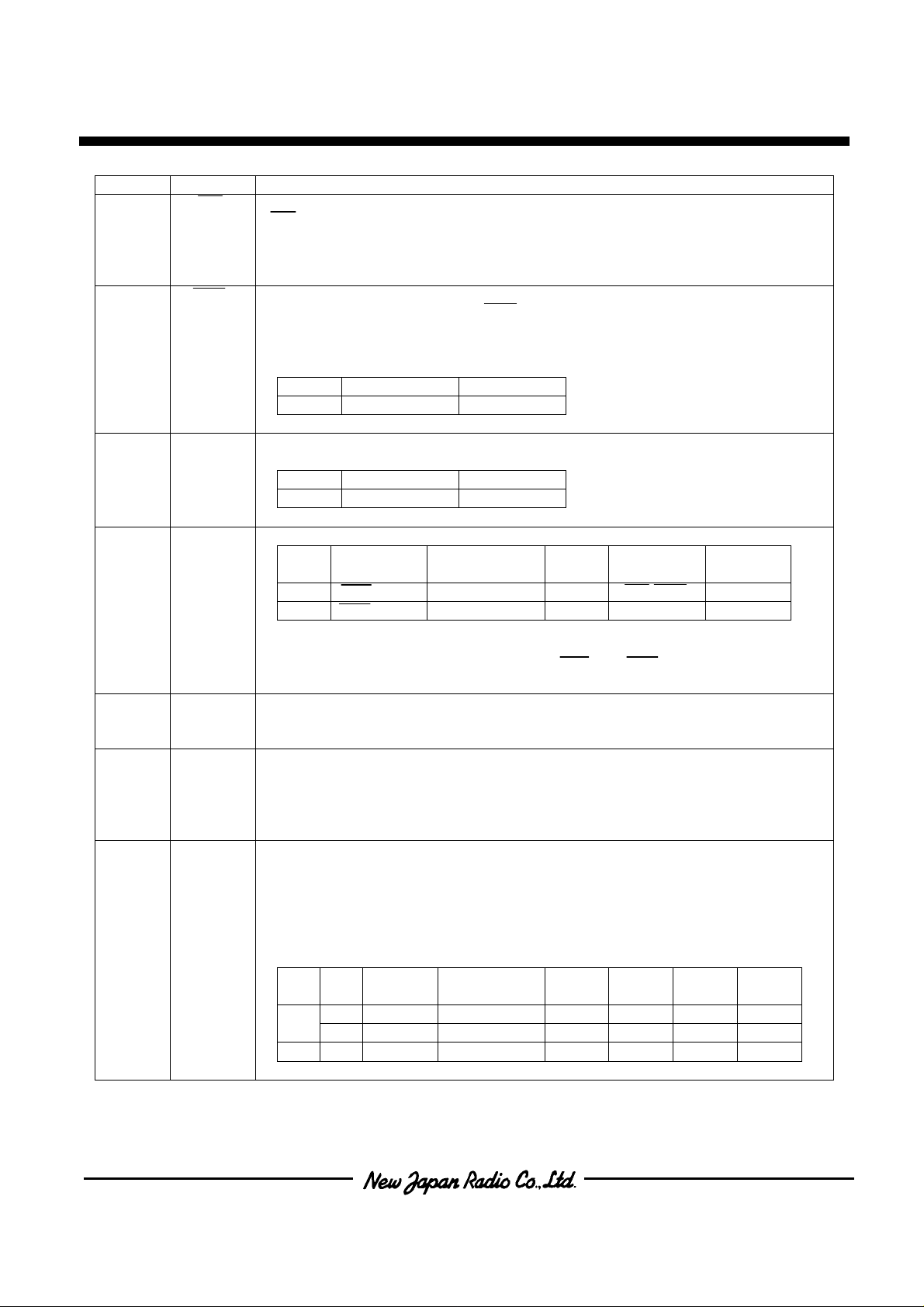
Functional description
■
(1) Block circuits description
(1-1) Busy Flag (BF)
During internal operation, the LSI is being busy and can’t accept any instructions except “status
read”. The BF data is output through D7 terminal by the “status read” instruction.
When the cycle time (tcyc) mentioned in the “AC characteristics” is satisfied, the BF check isn’t
required after each instruction, so that MPU processing performance can be improved.
(1-2) Initial display line register
The initial display line register assigns a DDRAM line address which corresponds to COM0 by
“initial display line set” instruction. It is used for not only normal display but also vertical display
scrolling and page switching without changing the contents of the DDRAM.
However, the 65
(1-3) Line counter
The line counter provides a DDRAM line address. It initializes its contents at the switching of frame
timing signal (FR), and also counts-up in synchronization with common timing signal.
(1-4) Column address counter
The colum n addres s counter is an 8-bit preset counter which provide s a DDRAM column add ress,
and it is independent of below-mentioned page address register.
It will increment (+1) the column address whenever “display data read” or “display data write”
instructions are issued. However, the counter will be locked when no-existing address above (84)H
are addressed. The count-lock will be able to be released by the “column address set” instruction
again. The counter can invert the correspondence between the column address and segment driver
direction by means of “ADC set” instruction.
(1-5) Page address register
The page add r ess r egister pro vid e s a DDRA M page add re ss .
The last page address “8H” should be used for icon display because the only D0 is valid.
(1-6) Display data RAM (DDRAM)
The DDRAM contains 8,580-bit, and stores display data which is 1-to-1 correspondent to LCD panel
pixels.
When normal display mode, the display data “1” turns on and “0” turns off LCD pixels. When
inverse display mode, “1” turns off and “0” turns on.
th
address for icon display can’t be assigned for initial display line address.
- 10 -
Ver.2004-03-01
Page 11
NJU6676
Fig.1 Display data RAM (DDRAM) Map
Page Address Data Display Pattern Line
D0 (00)H COM0
D1 01 COM1
D3,D2,D1,D0 D2 02 COM2
(0,0,0,0) D3 Page 0 03 COM3
D4 04 COM4
D5 05 COM5
D6 06 COM6
D7 07
D0
D1
D3,D2,D1,D0 D2
(0,0,0,1) D3
D4
D5
D6
D7 0F COM15
D0 10 COM16
D1 11 COM17
D3,D2,D1,D0 D2 12 COM18
(0,0,1,0) D3 Page 2 13 COM19
D4 14 COM20
D5 15 COM21
D6 16 COM22
D7 17 COM23
D0 18 COM24
D1 19 COM25
D2 1A COM26
: : : : :
: : : : :
: : : : :
: : : : :
D5 35 COM53
D6 36 COM54
D7 37 COM55
D0 38 COM56
D1 39 COM57
D3,D2,D1,D0 D2 3A COM58
(0,1,1,1) D3 Page 7 3B COM59
D4 3C COM60
D5 3D COM61
D6 3E COM62
D7 3F COM63
(1,0,0,0) D0 Page 8 * COMM
Column ADC “0”
Address “1”
Segment Drivers
Note) COMM is independent of the “Initial display line set” inst ruction and always corresponds to the 65th line.
■
■
■ ■
■
■
■
■
00 01 02 03 04 05 06 82 83
83 82 81 80 7F 7E 7D 01 00
0 1 2 3 4 5 6
■
■ ■
■
■
■
■
■
■
08 COM8
09 COM9
0A COM10
Page 1 0B COM11
0C COM12
0D COM13
0E COM14
Address
130 131
Common
Initial
For example the Initial
display is 08H.
Driver
COM7
Ver.2004-03-01
-11-
Page 12
NJU6676
(1-7) Common direction register
The common direction register specifies common driver’s scanning direction.
Table 1.
A3
0 COM0 COM31 COM63 COM32
1 COM63 COM32 COM0 COM31
(1-8) Reset circuit
The reset circuit initializes the LSI to the following status by using of the reset signal into the RES
terminal.
Reset status using the RES terminal:
1. LCD Driver Set off
2. Display off
3. Normal Display (Non-inverse display)
4. ADC select : Normal mode (D0=0 )
5. Power control register clear
6. Serial interface register clear
7. LCD bias select : 1/9 bias
8. Entire display off : Normal mode
9. Read modify write off
10. Static indicator off
11. Initial display line address : (00)H
12. Column address : (00)H
13. Page address : (0) page
14. Common direction register : Normal mode (D3=0)
15. EVR mode off and EVR register : (20)H
The RES terminal should be connected to MPU’s reset terminal, and the reset operation should be
executed at the same timing of the MPU reset.
As described in the “DC characteristics”, it is necessary to input 1.5us(min.) or over “L” level signal
into the RES terminal in order to carry out the reset operation. The LSI will return to normal
operation after about 1.5us(max.) from the rising edge of the rest signal.
In case of using external power supply for LCD driving voltage, the RES terminal is required to be
being “L” level when the external power supply is turned-on.
The “Reset” instruction in Table.4 can’t be substituted for the reset operation by using of the RES
terminal. It executes above -mentioned only 9 to 15 items.
(1-9) LCD driving circuits
a) Common and segment drivers
LCD drivers consist of 64-common drivers, 132-segment divers and 1-icon-common driver.
As shown in “ ■ LCD driving waveform”, LCD driving waveforms are generated by the combination
of display data, common timing signal and internal FR timing signal.
Common drivers Register
PAD No.
Pin name
108 77 275 244
C0 C31 C63 C32
- 12 -
Ver.2004-03-01
Page 13
NJU6676
b) Display data latch circuit
The display data latch circuit temporally stores 132-bit display data transferred from the DDRAM in
the synchronization with the common timing signal, and then it transfers these stored data to the
segment drivers.
“Display on/off”, “inverse display on/off” and “entire display on/off” instructions control only the
contents of this latch circuit, they can’t change the contents of the DDRAM.
In addition, the LCD display isn’t affected by the DDRAM accuses during its displaying because the
data read-out timing from this latch circuit to the segment drivers is independent of accessing timing
to the DDRAM.
c) Line counter and latch signal or latch Circuits
The clock line counter and latch signal to the latch circuits are generated from the internal display
clock (CL). The line address of display data RAM is renewed synchronizing with display clock (CL).
132bits display data are latched in display latch circuits synchronizing with display clock, and then
output to the LCD driving circuits. The display data transfer to the LCD driving circuits is executed
independently with RAM access by the MPU.
d) Display timing generator
The display timing generates the timing signal for the display system bay combination of the master
clock CL and driving signal FR ( refer to Fig.2 ) The frame signal FR and LCD alternative signal
generate LCD driving waveform on the two frame alternative driving method.
e) Common timing generation
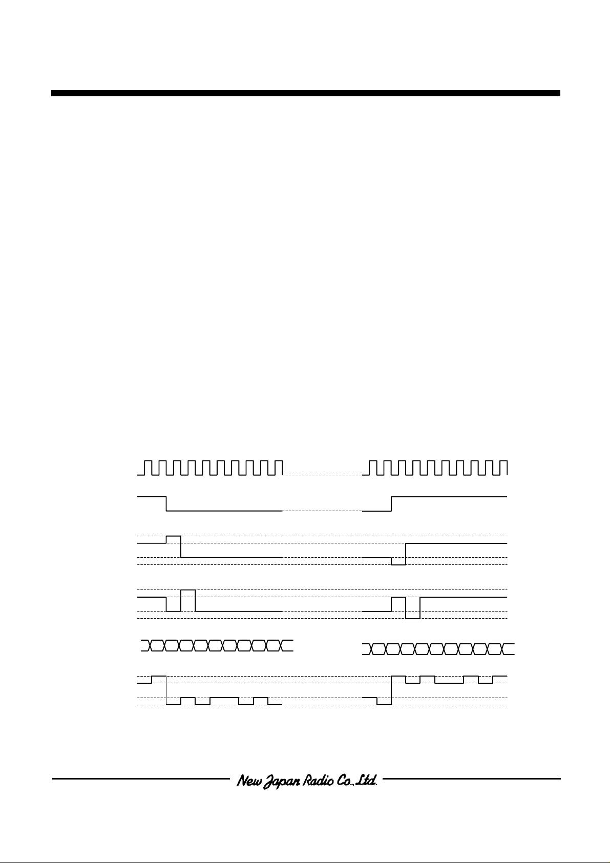
The common timing is generated by display clock CL (refer to Fig.2)
CL
64 65 1 2 3 4 5 6 7 8 64 65 1 2 3 4 5 6 7 8
FR
COM0
COM1
RAM data
SEG n
Fig.2 Wa veform of Disp la y Timing
Ver.2004-03-01
-13-
Page 14
NJU6676
f) Osci ll at or
This is the low power consumption CR oscillator which provides the display clock and voltage
converter timing clock.
g) Internal power circuits
The internal power circuits are composed of x4 boost voltage converter, output voltage regulator
including 64-step EVR and voltage followers.
The optimum values of the external passive components for the internal power circuits, such as
capacitors for V1 to V5 terminals and feed back resistors for VR terminal, depend on LCD panel
size. Therefore, it is necessary to evaluate the actual LCD module with these external components
in order to determine the optimum values.
Each portion of the internal power circuits is controlled by “power control set” instruction as shown
in Table.2. In addition, the combination of power supply circuits is described in Table.3.
Table.2) Power control set
Bits Portions Status
D2 Voltage converter 1 :On 0: Off
D1 Voltage regulator 1 :On 0: Off
D0 Voltage followers 1 :On 0: Off
Table.3) Power supply combinations
Status D2 D1 D0 Voltage
Using all internal power circuits 1 1 1 On On On Vss2 Use
Using voltage regulator and
Voltage followers
Using voltage follower s 0 0 1 Off Off On Vout, V5,
Using only extern al power supply 0 0 0 Off Off Off Vout,
0 1 1 Off On On Vout, Vss2 Open
converter
Note1) Ca pacitor input terminals: C1+, C1-, C2+ , C2-, C3Note2) Do not use other combinations except examples in Table.3.
Note3) Connect decoupling capacitors on V1 to V5 terminals whenever using the voltage followers.
Voltage
regulator
Voltage
followers
External
voltage
Vss2
V1 to V5
Capacitor
terminals
Open
Open
- 14 -
Ver.2004-03-01
Page 15
NJU6676
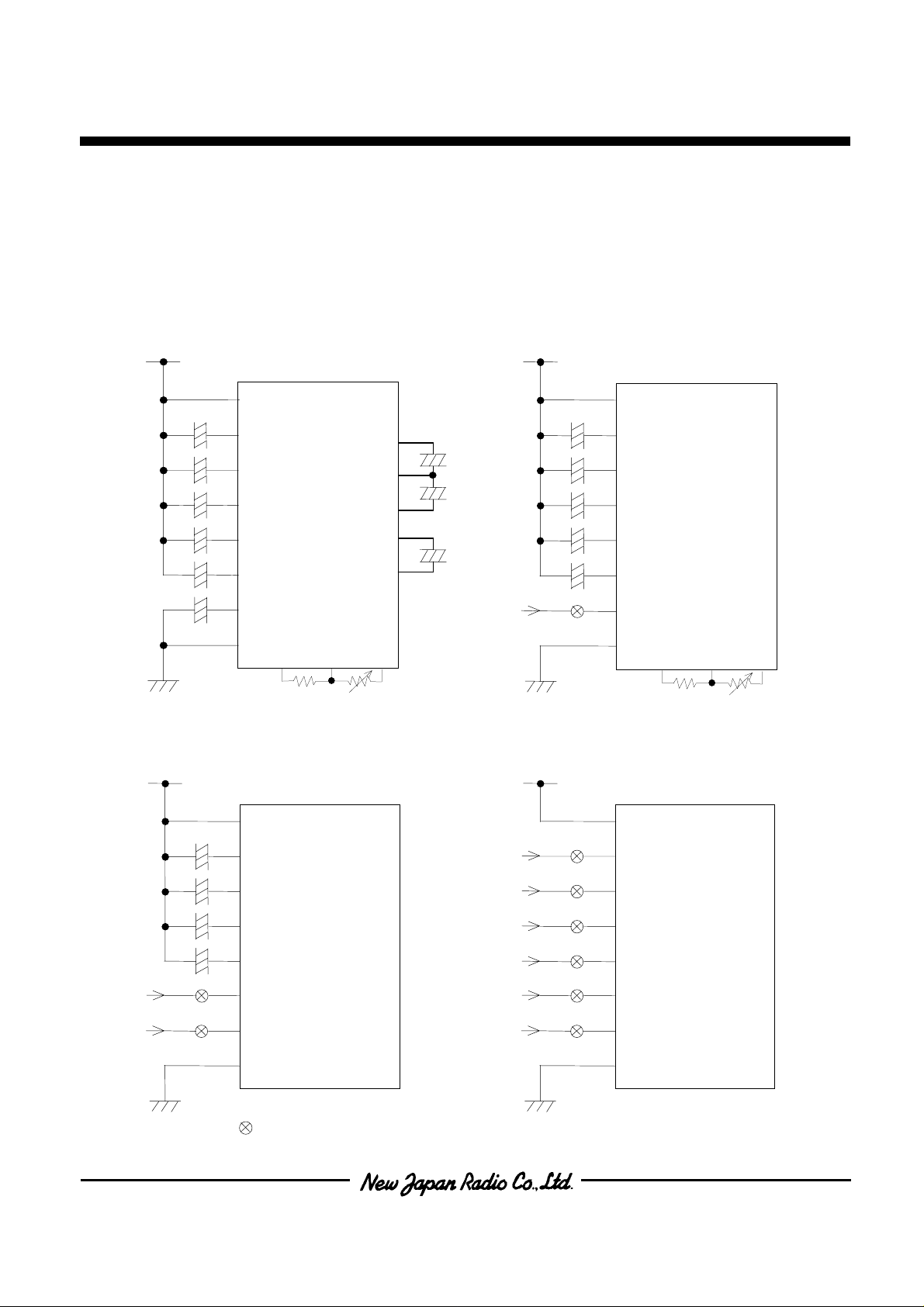
- Power Supply applications
Power Control Instruction
D2 : Boost Circuit
D1 : Voltage Regulator
D0 : Voltage Follower
1) Internal power supply Example. 2) Only V
All of the Internal Booster, Voltage Regulator, Internal Voltage Regulator,
Voltage Follower using. Voltage Follower using.
(D2,D1,D0) = (1,1,1) (D2,D1,D0) = (0,1,1)
+
+
+
+
+
+
V
V
V
V
V
V
V
DD
1
2
3
4
5
OUT
+
+
+
+
+
C1
C1
C3
C2
C2
-
+
-
+
-
+
+
V
SS2
V
DD
VR
V
5
3) V
and V5 Supply from outside Example. 4) External Power Supply Example.
OUT
Internal Voltage Follower using. All of V
(D2,D1,D0) = (0,0,1) (D2,D1,D0) = (0,0,0)
+
+
+
+
V
V
V
V
V
V
V
DD
1
2
3
4
5
OUT
V
SS2
: These switches should be open during the power save mode.
Supply from outside Example.
OUT
V
DD
V
1
V
2
V
3
V
4
V
5
V
OUT
V
SS2
to V5 and V
1
V
DD
V
1
V
2
V
3
V
4
V
5
V
OUT
V
SS2
V
VR
DD
supply from outside
OUT
V
5
Ver.2004-03-01
-15-
Page 16

NJU6676
(2) Instruction set
The D7 to D0 data is distinguished as display data or instruction data by the combination of A0, RD
and WR signals.
Table.4 Instruction table
Instruction code Instruction
AO RD WR
a Display On/Off 0 1 0 1 0 1 0 1 1 1 0/1 0 :Off
b Initial display line set 0 1 0 0 1 D5 D4 D3 D2 D1 D0 Specify DDRAM line
c Page address set 0 1 0 1 0 1 1 D3 D2 D1 D0 DDRAM page address
d Column address set
Upper 4-bit
Column address set
Lower 4-bit
e Status read 0 0 1 D7 D6 D5 D4 0 0 0 0 Read internal status
f Dis play data write 1 1 0 D7 D6 D5 D4 D3 D2 D1 D0 Write DDARM data
g Display data read 1 0 1 D7 D6 D5 D4 D3 D2 D1 D0 Read DDRAM data
h ADC select 0 1 0 1 0 1 0 0 0 0 0/1 Select segment direction
i Inverse display On/Off 0 1 0 1 0 1 0 0 1 1 0/1 0 : Normal display
j Entire display On/Off 0 1 0 1 0 1 0 0 1 0 0/1 0 : Normal display
k LCD bias select 0 1 0 1 0 1 0 0 0 1 0/1 0 : 1/9 bias
l Read modify write 0 1 0 1 1 1 0 0 0 0 0 Increment column address
m End 0 1 0 1 1 1 0 1 1 1 0 Release read modify write
n Reset 0 1 0 1 1 1 0 0 0 1 0 Internal reset
o Common direction select 0 1 0 1 1 0 0 0/1 * * * Select common direction
p Power control set 0 1 0 0 0 1 0 1 D2 D1 D0 Set the status of internal
q Driver On/Off 0 1 0 1 1 1 0 0 1 1 0/1 0 : Driver Off
r EVR mode set
EVR register set
s Static indicator On/Off
Static indicator register
set
t Power save mode On/Off 0 0 1 1 0 0 1 1 0 0 1 1 0 0 1 0 1 1 1 0 0 1 Dual commands of display
0
0
1
0
1
0
1
0
1
0
1
1
D7 D6 D5 D4 D3 D2 D1 D0
0
0
0
0
1
D3
D2
0
0
0
0
0
D3
D2
0
1
0
0
0
0
0
0
*
*
D5
D4
D3
D2
0
1
0
1
0
1
1
0
*
*
*
*
*
*
D1
D0
D1
D0
0
1
D1
D0
0
0/1
D1
D0
Description
1 :On
address for COM0
DDRAM column address
of upper 4-bits
DDRAM column address
of lower 4-bits
1 : Inverse display on
1 : Entire display on
1 : 1/7 bias
power circuits
1 : Driver On
Set EVR mode
Set EVR register
0 : Off
1 : On
Set static indicat or regis ter
Off & entire display On
- 16 -
Ver.2004-03-01
Page 17

NJU6676
(2-1) Instruction description
(a) Display On/Off
This instruction selects di splay turn-on or turn-off regardless of the contents of the DDRAM.
A0 RD WR D7 D6 D5 D4 D3 D2 D1 D0 Display On or Off
0 1 0 1 0 1 0 1 1 1 0
1
0 :Off
1 :On
(b) Initial display line set
This instruction specifies the DDRAM line address which corresponds to the COM0 position.
By means of repeating this instruction, the initial display line address will be dynamically changed; it
means smooth display scrolling will be en abled.
A0 RD WR D7 D6 D5 D4 D3 D2 D1 D0 Line address for COM0 (HEX)
0 1 0 0 1 0
0
0
0
0
0
0
0
:
:
1
1
1
1
0
:
:
1
1
1
1
0
0
1
:
1
1
:
0
1
00
01
:
3E
3F
(c) Page address set
In order to access to the DDRAM for writing or reading display data, both “page address set” and
“column address set” instructions are required before accessing.
The last page address “8” should be used for icon display because the only D0 is valid.
A0 RD WR D7 D6 D5 D4 D3 D2 D1 D0 Page address
0 1 0 1 0 1 1 0
0
0
0
0
:
:
0
1
1
0
0
0
1
:
1
0
:
1
0
0
1
:
7
8
Ver.2004-03-01
-17-
Page 18

NJU6676
(d) Column address set
As above-mentioned, in order to access to the DDRAM for writing or reading display data, it is
necessary to execute both “page address set” and “column address set” before accessing. The 8-bit
column address data will be valid when both upper 4-bit and lower 4-bit data are set into the column
address register.
Once the column address is s et, it will automat ically increment ( +1) whenever the DDRAM will be
accessed, so that the DDRAM will be able to be continuously accessed without “column address set”
instruction.
The column address will stop increment and the page address will not be changed when the last
address (83)H is addressed.
A0 RD WR D7 D6 D5 D4 D3 D2 D1 D0
0 1 0 0 0 0 1 0 A7
A7 A6 A5 A4 A3 A2 A1 A0 Column address (HEX)
0
0
0
0
0
:
1
1
:
0
0
0
0
0
:
:
0
0
0
0
(e) Status read
This inst ru ction read s out th e int ernal stat us re gar ding “bu sy f lag” , “A DC sele ct” , “ displ ay on/o ff” and
“reset”.
A0 RD WR D7 D6 D5 D4 D3 D2 D1 D0
0 0 1
BUSY ADC On/Off RESET
BUSY : When D7 is “1”, the LSI is being busy and can’t accept any instructions.
ADC : It shows the correspondence between the column address and segment drivers.
When D6 is “0”, the column address (131-n) corresponds to segment driver n.
When D6 is “1”, the column address (n) corresponds to segment driver n.
Please be careful that read out data is opposite of “ADC select” instruction data.
On/Off : It shows display on or off status.
When D5 is “0”, the LSI is in display-on status.
When D5 is “1”, the LSI is in display-off status.
Please be careful that read out data is opposite of “Display On/Off” instruction data.
RESET : It shows reset status.
When D4 is “0”, the LSI is in normal operation.
When D4 is “1”, the LSI is during reset operation.
(f) Display data write
This instruction writes display data into the selected column address on the DDRAM.
The column address automatically increments (+1) whenever the display data is written by this
instruction, so that this instruction can be continuously issued without “column address set”
instruction.
A0 RD WR D7 D6 D5 D4 D3 D2 D1 D0
1 1 0 Write Data
A3
0
0
:
0
0
A6
A5
A4
A2
A1
0
0
0
0
:
0
0
:
1
1
0 0 0 0
A0
0
1
:
0
1
Upper 4-bit
Lower 4-bit
00
01
:
82
83
- 18 -
Ver.2004-03-01
Page 19

NJU6676
(g) Display data read
This instruction reads out the display data stored in the selected column address on the DDRAM.
The column address automatically increments (+1) whenever the display data is read out by this
instruction, so that this instruction can be continuously issued without “column address set”
instruction.
After the ”column address set” instruction, a dummy read will be required, please refer to the (4-4).
In case of using serial interface mode, this instruction can’t be used.
A0 RD WR D7 D6 D5 D4 D3 D2 D1 D0
1 0 1 Read Data
(h) ADC select
This instruction selects segment driver direction.
The correspondence between the column address and segment driver direction is shown in Fig.1.
A0 RD WR D7 D6 D5 D4 D3 D2 D1 D0 Segment driver direction
0 1 0 1 0 1 0 0 0 0 0
1
Normal
Inverse
(i) Inverse display On/Off
This instruction inverses the status of turn-on or turn-off of entire LCD pixels. It doesn’t change the
contents of the DDRAM.
A0 RD WR D7 D6 D5 D4 D3 D2 D1 D0 Display status
0 1 0 1 0 1 0 0 1 1 0
1
Normal
Inverse
(j) Entire display On/Off
This instruction turns on entire LCD pixels regardless the contents of the DDRAM. It doesn’t change
the contents of DDRAM.
A0 RD WR D7 D6 D5 D4 D3 D2 D1 D0 Entire display on/off
0 1 0 1 0 1 0 0 1 0 0
1
Normal
Entire display on
(k) LCD bias set
This instruction selects LCD bias value.
A0 RD WR D7 D6 D5 D4 D3 D2 D1 D0 LCD bias
0 1 0 1 0 1 0 0 0 1 0
1
1/9
1/7
Ver.2004-03-01
-19-
Page 20

NJU6676
(l) Read modify write
This instruction controls column address increment.
By using of this instruction, the column address can’t increment when read operation but it can
increment when write operation. This status will be continued until the below-mentioned “end”
instruction will be issued.
This instruction can reduce the load of MPU, during the display data in specific DDRAM area is
repeatedly changed for cursor blink or others.
A0 RD WR D7 D6 D5 D4 D3 D2 D1 D0
0 1 0 1 1 1 0 0 0 0 0
The sequence of cursor blink display
No
Page Address Set
Column Address Set
Read Modify Write
Dummy Read
Data Read
Data Write
Dummy Read
Data Read
Data Write
Dummy Read
Data Read
Data Write
End
Finish?
Yes
Set to the Start Address of
Cursor Display
Start the Read Modify Write
The data is ignored
Column Counter doesn’t increase
Data inverse by MPU
Column Counter increase
Column Counter doesn’t increase
Column Counter doesn’t increase
Column Counter increase
Column Counter doesn’t increase
Column Counter doesn’t increase
Column Counter increase
End the Read Modify Write
- 20 -
Ver.2004-03-01
Page 21

NJU6676
A
(m) End
The “end” instruction cancels the read modify write mode and makes the column address return to
the initial value just before “read modify write” is started.
A0 RD WR D7 D6 D5 D4 D3 D2 D1 D0
0 1 0 1 1 1 0 1 1 1 0
Column
ddress
N N+m N+3N+2N+1 N
Return
Read modify write
End
(n) Reset
This instruction reset the LSI to the following status, however it doesn’t change the contents of the
DDRAM. Please be careful that it can’t be substituted for the reset operation by using of the RES
terminal.
Reset status by “reset” instruction:
1. Read modify write off
2. Static indicator off
3. Initial display line address : (00)H
4. Column address : (00)H
5. Pag e ad d res s : (0) page
6. Common direction register : Normal mode (D3=0)
7. EVR mode off and EVR register : (20)H
A0 RD WR D7 D6 D5 D4 D3 D2 D1 D0
0 1 0 1 1 1 0 0 0 1 0
(o) Common driver direction select
This instruction selects common driver direction.
Please refer to (1-7) common driver direction for more detail.
A0 RD WR D7 D6 D5 D4 D3 D2 D1 D0 Common driver direction
0 1 0 1 1 0 0 0 1 * * * Normal
Inverse
Ver.2004-03-01
-21-
Page 22

pply
pply
NJU6676
(p) Power control set
This instruction controls the status of internal power circuits. Please refer to the (1-9) LCD Driving
Circuits (g) internal power circuits for more detail.
A0 RD WR D7 D6 D5 D4 D3 D2 D1 D0 Status
0 1 0
Note) The internal power supply must be Off when external power supply using.
* The wait time depends on the C 4 to C8, COU T capacitors, and VDD and VLCD Voltage.
Therefore it requires the actual evaluation usin g the LCD modul e to get the correct time.
(q) LCD Driver O n/Off
This instruction controls LCD driving waveform output through the COM/SEG terminals.
A0 RD WR D7 D6 D5 D4 D3 D2 D1 D0 Driver
0 1 0 1 1 1 0 0 1 1 0
The NJU6676 contains low power LCD driving voltage generator circuit reducing own operating
current. Therefore , it requires the following sequence procedures at power on for power source
stabilized operation.
LCD Driving power sup ply On/Off sequences
The following sequences required wh en the po w e r suppl y is turned On/Off.
When the power supply is turned on again after the turn off (by the power save instruction), the power
save release sequence(t) is required.
Turn ON sequence Turn OFF sequence
0 0 1 0 1 0 1 Voltage converter off
0 1 Voltage regulator off
0
Common Direction Select
Static Indicator Set
EVR Register Set
Internal Power Supply ON
External Power Su
Or
ON
Wait Time
LCD Driver ON
1
1
Entire Display OFF
Internal Power Supply OFF
External Power Su
NJU6676 Power OFF
Voltage converter on
Voltage regulator on
Voltage followers off
Voltage followers on
Off
On
Display OFF
Or
OFF
LCD Driver OFF
- 22 -
Ver.2004-03-01
Page 23

NJU6676
(r) EVR set
1) EVR mode set
This instruction sets the LSI into the EVR mode, and it is always used by the combination with “EVR
register set”.
The LSI can’t accept any instructions except the “EVR register set” during the EVR set mode. This
mode will be released after the “EVR register set” instruction.
A0 RD WR D7 D6 D5 D4 D3 D2 D1 D0
0 1 0 1 0 0 0 0 0 0 1
2) EVR register set
This instruction sets 6-bit data into the EVR register to determine the output voltage “V5” of the
internal voltage regulator.
A0 RD WR D7 D6 D5 D4 D3 D2 D1 D0 V5
0 1 0 * * 0
0
0
0
0
0
0
0
:
:
1
1
1
1
0
;
:
1
1
1
1
0
0
1
:
1
1
:
0
1
Minimum
:
:
:
Maximum
(s) Static indicator
1) Static indicator on/off
This instruction selects static indicator turn-on or turn-off, and it is always used by the combination
with the “ static indicator register set”.
A0 RD WR D7 D6 D5 D4 D3 D2 D1 D0 Static indicator
0 1 0 1 0 1 0 1 1 0 0
1
Off
On
2) Static indicator register set
This instruction sets 2-bit data into the static indicator register.
A0 RD WR D7 D6 D5 D4 D3 D2 D1 D0 Status
0 1 0 * * * * * * 0
0
0
1
1
Off
1
On (Blink at 1.0s intervals)
0
On (Blink at 0.5s intervals)
1
On (Turn on at all time)
Ver.2004-03-01
-23-
Page 24

NJU6676
(t) Power save mode On/Off
This instruction sets the LSI into the power save mode by the combination of “display off” and “entire
display on” instructions for reducing operating current as well as static operation’s.
The internal status and the contents of the DDRAM will be remained just before the “power save
mode on/off” instruction. In addition, the DDRAM can be accessed during the power save mode.
There are two power save modes, sleep mode and standby mode.
During sleep mode:
All LCD system stops as follows,
1. Oscillator and internal power circuits stop.
2. All common and segment drivers output VDD level.
During standby mode:
The LCD system except the static indicator stops as follows,
1. Oscillator and internal power circuits stop.
2. All common and segment drivers output VDD level.
3. The only static indicator is working.
The sequence of power save mode
Static indicator off Static indicator on
Power save on (Dual instructions)
Sleep mode Standby mode
Power save off
Entire display off
Static indicator on
Release Sleep mode Release Standby mode
+
Power save off
Entire display off
- 24 -
Ver.2004-03-01
Page 25

NJU6676
(3) Internal power circuits
(3-1)Voltage converter
The voltage converter generates maximum 4x boosted negative-voltage from the voltage between
VDD and Vss2. The boosted voltage is output from the VOUT terminal.
The internal oscillator is required to be operating when using this converter, because the divided
signal provided from the oscillator is used for the internal timing of this circuit.
The boosted voltage between VDD and Vout must not exceed 18.0V.
The voltage converter requires external capacitors for boosting as shown in below.
The capacitors connection for the vol tage regulator:
4x boost 3x boost 2x boost
+
+
+
VDD
Vss2
Vout= 4x (VDD-Vss2)
Vss2
Vout
C3C1+
C1-
C2-
C2+
+
+
+
VDD
Vss2
Vout= 3x (VDD-Vss2)
Vss2
Vout
C3C1+
C1-
C2-
C2+
+
+
VDD
Vss2
Vout= 2x (VDD-Vss2)
Vss2
Vout
C3C1+
C1-
C2-
C2+
Ver.2004-03-01
-25-
Page 26

NJU6676
(3-2)Contrast control using the voltage regulator
The voltage regulator determines the LCD driving voltage “V5” according to the Rb/Ra ratio and
VREG voltage. The equations to calculate V5 are as follows:
Voltage regulator
VDD
Ra
VREG
VLCD
VR
+
-
V5
Rb
Vout
Fig.3 Voltage regulator circuit
VLCD = VDD – V5
= (1+Rb/Ra) x VREG ---[1]
VREG = (n/162) x (VDD-Vss2) ---[2]
VLCD : LCD driving voltage
Ra, Rb : Feed back resistors
VREG : Contrast control voltage
n : Parameter decided instruction
(3-3)Contrast control voltage VREG
As the equation [2] shows, the VREG value depends on the parameter “n”. The “n” is selected a
value within 99 to 162 by using of “EVR register set” instruction as shown below.
The relationship between EVR register and VLCD level
Register value
00H 0 0 0 0 0 0 99
01H 0 0 0 0 0 1 100
02H 0 0 0 0 1 0 101
: : : : : : : : :
3DH 1 1 1 1 0 1 160
3EH 1 1 1 1 1 0 161
3FH 1 1 1 1 1 1 162
D5 D4 D3 D2 D1 D0 n VREG
(99/162) x (VDD-Vss2)
(100/162) x (VDD-Vss2)
(101/162) x (VDD-Vss2)
(160/162) x (VDD-Vss2)
(161/162) x (VDD-Vss2)
(162/162) x (VDD-Vss2)
Minimum
:
:
:
:
Maximum
- 26 -
Ver.2004-03-01
Page 27

- VLCD set ting example
We recommend the total value of Ra and Rb is between 1MΩ and 5MΩ. When using Ra=1MΩ,
Rb=3MΩ and VDD=3V, the VLCD is calculated as follows:
The minimum VLCD:
VLCD =(1+Rb/Ra) X VREG
=(1+3/1) X [(99/162) X 3.0]
=7.33V
The maximum VLCD:
VLCD =(1+Rb/Ra) X VREG
=(1+3/1) X [(162/162) X 3.0]
=12.0V
NJU6676
Ver.2004-03-01
-27-
Page 28

JU6676
JU6676
NJU6676
(3-4) LCD Driving Voltage Generation Circuits
The LCD driving bias voltage of V1,V2,V3,V4 are generated internally by dividing the VLCD
(VLCD=VDD- V 5) volta ge with th e int e r na l bl eed er resista nc e . An d it is s u ppli ed to the LCD driving
circuits after the impedance conversion with voltage follower circuit.
As shown in Fig 4, Five capacitors are required to connect to each LCD driving voltage terminal for
voltage stabilizing. And the value of capacitors C4, C5, C6, C7, and C8 are determined depending
on the actual LCD panel display evaluation.
Using the internal Power Supply Using the external Power Supply
C1
+
VSS
VSS2
C1C1+
VSS
C1C1+
C3
Cout
+
+
C2
C3C2+
C2-
C3C2+
C2-
R3
VOUT
V5
N
*
VOUT
V5
N
R2
*
VR
VR
R1
+
+
+
+
+
C4
C5
C6
C7
C8
VDD
V1
V2
V3
V4
V5
External
Voltage
Generator
VDD
V1
V2
V3
V4
V5
Fig 4
*1 Short wiring or sealed wiring to the VR terminal is
required due to the high impedance of VR terminal.
*2 Following connection of VOUT is required when external
power supply using.
When VSS > V5 --- VOUT=V5
When VSS < V5 --- VOUT=VSS
Reference set up value
VLCD=VDD-V5=6.0 to 7.5V
∼
COUT
C1 ∼ C3, C8
C4 ∼ C7
R1
R2
R3
1.0uF
∼
1.0uF
0.1∼0.47uF
2MΩ
500KΩ
2.5MΩ
- 28 -
Ver.2004-03-01
Page 29

)
NJU6676
(4) MPU interface
(4-1) Interface type selection
NJU6676 interfaces with MPU by 8-bit bidirectional data bus (D7 to D0) or serial (SI:D7). The 8 bit
parallel or serial interface is determined by a condition of the P/S terminal connecting to "H" or "L"
level as shown in Table 5. In case of the serial interface, status and RAM data read out operation is
impossible.
Table 5
“-“ : They should be fixed to “H” or “L”.
P/S Type
H Parallel
L Serial
CS1
CS1
CS1
A0
A0
A0 - - - SI SCL Hi-z
RD WR
RD WR
C86 SI(D7)
C86 D7 D6
SCL(D6
D0∼D5
D0∼D5
Parallel Interface
The NJU6676 interfaces to 68 or 80 type MPU directly when the parallel interface (P/S="H") is
selected. 68 type MPU or 80 is determined by the condition of C86 terminal connecting to "H" or "L"
as shown in table 6.
Table 6
C86 Type
H 68 type MPU
L 80 type MPU
CS1
CS1
CS1
A0
A0 E R/W
A0
RD WR
RD WR
D0∼D7
D0∼D7
D0∼D7
(4-2) Discrimination of Data Bus Signal
The NJU6676 discriminates the mean of signal on the data bus by the combination of A0, E, R/W,
and (RD,WR) signals as shown in Table 7.
Table 7
Commo
A0 R/W
68 type 80 type
n
RD WR
H H L H Read Display Data
H L H L Write Display Data
L H L H Status Read
L L H L Write into the Register(Instruction)
Function
Ver.2004-03-01
-29-
Page 30

NJU6676
(4-3) Serial Interface.(P/S="L")
Serial interface circuits consist of 8 bits shift register and 3 bits counter. SI and SCL input are
activated when the chip select terminal CS1 set to "L"and P/S terminal set to "L". The 8 bits shift
register and 3 bits counter are reset to the initial condition when the chip is not selected. The data
input from SI terminal is MSB first like as the order of D7,D6,- - - - D0, and the data are entered into
the shift register synchronizing with the rise edge of the serial clock SCL. The data in the shift
register are converted to parallel data at the 8th serial clock rise edge input. Discrimination of the
display data or inst r ucti on o f t he s er ial in put da ta i s exe cut ed b y th e co ndi ti on o f A 0 at t he 8t h se rial
clock rise edge. A0="H" is display data and A0="L" is instruction. When RES terminal becomes "L"
or CS1 terminal becomes "H" before 8th serial clock rise edge, NJU6676 recognizes them as a
instruction data incorrectly. Therefore a unit of serial data must be structured by 8-bit. The time
chart for the serial interface is shown in Fig. 5. To avoid the noise trouble, the short wiring is
required for the SCL input.
Note) The read out function, such as the status or RAM data read out, is not supported in this
serial interface
CS1
CS2
SI
D7 D6 D5 D4 D3 D2 D1 D0 D7
SCL
1 2 3 4 5 6 7 8 9 10
A0
Fig.5
- 30 -
Ver.2004-03-01
Page 31

NJU6676
(4-4) Access to the Display Data RAM and Internal Register.
The NJU6676 is operating as one of pipe-line processor by the bus-holder connecting to the internal data bus
to adjust the operation frequency between MPU and the Display Data RAM or Internal Register.
For example, when the MPU reads out the data from the Display Data RAM, the read out data in the data read
cycle (dummy read) is held in the bus-holder, then it is read out from the bus-holder to the system bus at the
next data read cycle. When the MPU writes the data into the Display Data RAM, the data is held in the busholder , then it is writt en int o t he Di spla y Data RAM by the next data write cycle.
Therefore high speed data transmission between MPU and NJU6676 is available because of it is not limited by
the tACC and tDS as display data RAM access time and is limited by the sy stem cycle time (R) or (W).
If the cycle time is not be kept in the MPU operation, NOP should be inserted to the system instead of the
waiting operation.
The read out operation does not read out the data in the pointed address just after the address set operation.
And second read out operation can read out the data correctly from the pointed address.
Therefore, one dummy read operation is required after address setting or write cycle as shown in Fig. 6..
Write timing
MPU signal
WR
Data
N N+1 N+2 N+3
Internal signal
Bus holder
WR
N N+1 N+2 N+3
Read timing
WR
MPU signal
RD
Data
N N n n +1
Address
set
Dummy
read
Data read Data read
WR
Internal signal
RD
Column
address
Bus holder
N
N N+1 N+2
n n +1
Fig.6
Ver.2004-03-01
-31-
Page 32

NJU6676
(4-5) Chip select
CS1, CS2 are Chip Select terminals. In case of CS1="L" and CS2=”H”, the interface with MPU is
available. In case of CS1=”H” or CS2=”L”, the D0 to D7 are high impedance and A0, RD, WR,
D7(SI) and D6(SCL) inputs are ignored. If the serial interface is selected when CS1=”H” or CS2=”L”,
the shift register and the counter are reset. However, the reset is always operated in any conditions
of CS1 and CS2.
- 32 -
Ver.2004-03-01
Page 33

NJU6676
ABSOLUTE MAXIMUMN RATINGS
■
Ta=25°C
Parameter Symbol Ratings Unit
Supply voltage (1) VDD -0.3 to +7.0 V
Supply voltage (2) Vss2 -7.0 to+0.3
-6.0 to +0.3 (When using 3x voltage converter)
-4.5 to +0.3 (When using 4x voltage converter)
Supply voltage (3) V5
Vout
Supply voltage (4) V1,V2
V3,V4
Input voltage Vin -0.3 to VDD+0.3 V
Output voltage Vout -0.3 to VDD+0.3 V
Operating temperature Topr -30 to +80 °C
Storage temperature Tstg -55 to +100 (TCP)
- 55 to +125 (Chip)
-18.0 to +0.3 V
V5 to +0.3 V
V
°
C
VDD V
DD
V
SS
V
SS2
, V1 to V4
V
5
Note1) Vss2, V1 to V5, Vout voltage values are specified as VDD = 0V.
Note2) The relation of VDD>
V1>V2>V3>V4>V5>Vout ; VDD>Vss>Vout must be maintained.
In case of inputting external LCD driving voltage, LCD drive voltage should start supplying
to NJU6676 at the mean time of turning on VDD power supply or after turned on VDD.
In use of the voltage boost circuit, the condition that the supply voltage : 18V >
necessary.
VDD-Vout is
Note3) If the LSI are used on condition beyond the absolute maximum rating, the LSI may be
destroyed. Using LSI within electrical characteristics is strongly recommended for normal
operation. Use beyond the electric characteristics conditions will cause malfunction and
poor reliability.
Note4) Decoupling capacitor should be connected between VDD and Vss due to the stabilized
operation for the voltage converter.
Ver.2004-03-01
-33-
Page 34

NJU6676
DC Electrical Characteristics
■
VDD=2.7V to 3.3V, Vss=0V, Ta=-30 to +80°C
Parameter Symbol Conditions Min. Typ. Max. Unit Note
Power supply(1) VDD Recommend 2.7 - 3.3 V 5
Possible 2.2 - 5.5 V
Power supply(2) Vss2 VDD common -6.0 - -2.5 V
Power supply(3) V5 VDD common -18 - -6 V
V1,V2 0.4xV5 - VDD V
V3,V4 V5 - 0.6xV5 V
“H” level input voltage VIHC1 0.8VDD - VDD V
“L” level input volt age VILC1 Vss - 0.2VDD V
“H” level output voltage VOHC1 IOH=-0.5mA 0.8VDD - VDD V
“L” level output voltage VOLC1 IOL=0.5mA Vss - 0.2VDD V
Input leakage current ILI All input terminals -1.0 - 1.0 uA
Output leakage current ILO D0 to D7 terminals -3.0 - 3.0 uA
LCD on resistance
Input pin capacitance CIN
Oscillation frequency fOSC
Display clock frequency fCL External input 4.5 5.5 6.5 kHz
RON1 VLCD=14.0V,
Ta=25°C
RON2
VLCD=8.0V, Ta=25°C
Ta=25°C
VDD=3V, Ta=25°C
- 2.0 3.5
- 3.2 5.4
- 10 - pF 7
18 22 26 kHz
kΩ
kΩ
6
Internal power supply
Parameter Symbol Conditions Min. Typ. Max. Unit Note
Vss2
Voltage converter
Output voltage
Voltage converter
Output on resistance
Voltage regulator
Operating voltage
Voltage follower
Operating voltage
Operating current IDDQ1 When sleep mode - 0.01 5.0 uA 9
IDDQ2 When standby mode - 4 10 uA
IDD1 VDD=3V, V5=-11V - 80 140 uA
IDD2 Checker flag display - 20 40 uA
IDD3 Without MPU access - 18 35 uA
IDD4 All COM/SEG open - 15 30 uA
Reference Voltage V
Vout VDD common -18.0 - - V
RQUAD C1 to C3, Cout=1.0uF
Vout2 Voltage converter off
V5 Voltage regulator off
REG%
VDD common
Using 3x voltage
converter
VDD common
Using x4 voltage
converter
Using x4 booster
VDD=3V, Vss=Vss2
External power supply
External power supply
VDD=3V, Ta=25°C
-6.0 - -2.5 V Input voltage
-4.5 - -2.5 V
- 2.5 3.5
-18.0V - -6.0V V 8
-18.0V - -6.0V V
3.0 %
kΩ
Note5) Although the NJU6676 can operate in wide range of the operating voltage, it shall not be guaranteed
in a sudden voltage fluctuation during the access with MPU.
Note6) RON is the resistance values in supplying 0.1V voltage-difference between power supply terminals
(V1,V2,V3,V4) and each output terminals (common / segment). This is specified within the range of
Operating Voltage (2).
Note7) Apply to A0, D7 to D0, RD, WR, CS1, CS2, RES, C86 and P/S terminals.
Note8) The voltage adjustment circuit controls V5 within the range of the voltage follower operating voltage.
Note9) The value of after Driver Output On instruction execution. Each operating current shall be defined as
being measured in the following condition.
- 34 -
Ver.2004-03-01
Page 35

Symbol
Power Control Operating Condition
D2 D1 D0
Voltage
converter
Voltage
regulator
Voltage
followers
External
Voltage Supply
(Input Terminal)
IDD1 1 1 1 On On On Use(V
IDD2 0 1 1 Off On On Use(V
IDD3 0 0 1 Off Off On Use(V
IDD4 0 0 0 Off Off Off
OUT,V5,VSS2
Use(V
SS2
OUT,VSS2
OUT,V1
NJU6676
)
)
)
)
V
∼
5
Ver.2004-03-01
-35-
Page 36

NJU6676
IDD 1,2,3,4 measurement circuits:
IDD1
VDD
A
Vss Vout
IDD2
VDD
A
Vss
IDD3
VDD
A
Vss
IDD4
VDD
A
Vss
V5 VR
NJU6676
C2+ C1- C1+ C3-C2-
+ +
+
V5 VR
NJU6676
C2+ C1- C1+ C3-C2- Vout
V5 VR
NJU6676
C2+ C1- C1+ C3-C2- Vout
V1 V2 V3 V4
V4 V3 V2 V1
V5 VR
NJU6676
C2+ C1- C1+ C3-C2- Vout
- 36 -
Ver.2004-03-01
Page 37

,
NJU6676
BUS TIMING CHARACTERISTICS
■
Read and Write characteristics (80 type MPU)
tcyc8
A0,CS1,CS2
WR
RD
tCCH
tAW8 tAH8
tCCL
tDS8 tDH8
D7 to D0
Write
tf tr
tOH8 tACC8
D7 to D0
Read
(Vss=0V, VDD=4.5 to 5.5V, Ta=-30 to 80°C)
Parameter Terminal Symbol Condition Min. Max. Unit
Address hold time tAH8 0 - ns
Address set up time
System cycle time tcyc8 166 - ns
Control “L” pulse width (Write) tCCLW 30 - ns
Control “L” pulse width (Read) tCCLR 70 - ns
Control “H” pulse wi dth (Write) tCCHW 30 - ns
Control “H” pulse wi dth (Read)
Data set up time tDS8 30 - ns
Data hold time tDH8 10 - ns
RD access time t A CC8 - 70 ns
Output disable time
Input signal rising, falling edge
A0,CS1,
CS2
WR,RD
D7 ∼ D0
CS1,CS2
WR,RD,A0,
D7 ∼ D0
tAW8 0 - ns
tCCHR 30 - ns
tOH8
tr,tf 15 ns
CL=100pF
5 50 ns
Ver.2004-03-01
-37-
Page 38

NJU6676
(Vss=0V, VDD=2.7 to 4.5V, Ta=-30 to 80°C)
Parameter Terminal Symbol Condition Min. Max. Unit
Address hold time tAH8 0 - ns
Address set up time
System cycle time tcyc8 300 - ns
Control “L” pulse width (Write) tCCLW 60 - ns
Control “L” pulse width (Read) tCCLR 120 - ns
Control “H” pulse wi dth (Write) tCCHW 60 - ns
Control “H” pulse wi dth (Read)
Data set up time tDS8 40 - ns
Data hold time tDH8 15 - ns
RD access time t A CC8 - 140 ns
Output disable time
Input signal rising, falling edge
A0,CS1,
CS2
WR,RD
D7 ∼ D0
CS1,CS2
WR,RD,A0,
D7 ∼ D0
tAW8 0 - ns
tCCHR 60 - ns
tOH8
tr,tf 15 ns
CL=100pF
10 100 ns
(Vss=0V, VDD=2.2 to 2.7V, Ta=-30 to 80°C)
Parameter Terminal Symbol Condition Min. Max. Unit
Address hold time tAH8 0 - ns
Address set up time
System cycle time tcyc8 1000 - ns
Control “L” pulse width (Write) tCCLW 120 - ns
Control “L” pulse width (Read) tCCLR 240 - ns
Control “H” pulse wi dth (Write) tCCHW 120 - ns
Control “H” pulse wi dth (Read)
Data set up time tDS8 80 - ns
Data hold time tDH8 30 - ns
RD access time t A CC8 - 280 ns
Output disable time
Input signal rising, falling edge
A0,CS1,
CS2
WR,RD
D7 ∼ D0
CS1,CS2
WR,RD,A0,
D7 ∼ D0
tAW8 0 - ns
tCCHR 120 - ns
tOH8
tr,tf 15 ns
CL=100pF
10 200 ns
Note10) Each timing is specified based on 0.2xVDD and 0.8xVDD.
- 38 -
Ver.2004-03-01
Page 39

(H[
]
[
]
)
NJU6676
Read and Write characteristics (68 type MPU)
tAW6
tcyc6
・
R/W
L
tDS6
R/W
tEW
tr tf
tACC6
tAH6
tDH6
tOH6
E
A0,CS1,CS2
D7 to D0
Write
D7 to D0
Read
tEWL
(Vss=0V, VDD=4.5 to 5.5V, Ta=-30 to 80°C)
Parameter Terminal Symbol Condition Min. Max. Unit
Address hold time tAH6 0 - ns
Address set up time tAW6 0 - ns
System cycle time
Enable “H” pulse width (R ead) tEWHR 70 - ns
Enable “H” pulse width ( Write) tEWHW 30 - ns
Enable “L” pulse width (Read) tEWLR 30 - ns
Enable “L” pulse width (Write)
Data set up time tDS6 30 - ns
Data hold time tDH6 10 - ns
RD access time t A CC6 - 70 ns
Output disable time
Input signal rising, falling edge
A0,CS1,
CS2
E
D7 ∼ D0
E,R/W,A0,
D7 ∼ D0
tcyc6 166 - ns
tEWLW 30 - ns
tOH6
tr,tf 15 ns
CL=100pF
10 50 ns
Ver.2004-03-01
-39-
Page 40

NJU6676
(Vss=0V, VDD=2.7 to 4.5V, Ta=-30 to 80°C)
Parameter Terminal Symbol Condition Min. Max. Unit
Address hold time tAH6 0 - ns
Address set up time tAW6 0 - ns
System cycle time
Enable “H” pulse width (R ead) tEWHR 120 - ns
Enable “H” pulse width ( Write) tEWHW 60 - ns
Enable “L” pulse width (Read) tEWLR 60 - ns
Enable “L” pulse width (Write)
Data set up time tDS6 40 - ns
Data hold time tDH6 15 - ns
RD access time t A CC6 - 140 ns
Output disable time
Input signal rising, falling edge
A0,CS1,
CS2
E
D7 ∼ D0
E,R/W,A0,
D7 ∼ D0
tcyc6 300 - ns
tEWLW 60 - ns
tOH6
tr,tf 15 ns
CL=100pF
10 100 ns
(Vss=0V, VDD=2.2 to 2.7V, Ta=-30 to 80°C)
Parameter Terminal Symbol Condition Min. Max. Unit
Address hold time tAH6 0 - ns
Address set up time tAW6 0 - ns
System cycle time
Enable “H” pulse width (R ead) tEWHR 240 - ns
Enable “H” pulse width ( Write) tEWHW 120 - ns
Enable “L” pulse width (Read) tEWLR 120 - ns
Enable “L” pulse width (Write)
Data set up time tDS6 80 - ns
Data hold time tDH6 30 - ns
RD access time t A CC6 - 280 ns
Output disable time
Input signal rising, falling edge
A0,CS1,
CS2
E
D7 ∼ D0
E,R/W,A0,
D7 ∼ D0
tcyc6 1000 - ns
tEWLW 120 - ns
tOH6
tr,tf 15 ns
CL=100pF
10 200 ns
Note11) Each timing is specified based on 0.2xVDD and 0.8xVDD.
- 40 -
Ver.2004-03-01
Page 41

NJU6676
Write characteristics (Serial interface)
CS1,CS2
tCSS
tSAS
tCSH
tSAH
A0
SCL
tscyc
tSLW
tSHW
tSDH tSDS
SI
trtf
(Vss=0V, VDD=4.5 to 5.5V, Ta=-30 to 80°C)
Parameter Terminal Symbol Condition Min. Max. Unit
Serial clock cycle tscyc 200 - ns
SCL “H” pulse width tSHW 75 - ns
SCL “L” pulse width
Address set up time tSAS 50 - ns
Address hold time
Data set up time tSDS 50 - ns
Data hold time
CS1-SCL ti m e
Input signal rising, falling edge
SCL
A0
SI
CS1,CS2
SCL,A0,
CS1,CS2,SI
tSLW 75 - ns
tSAH 100 - ns
tSDH 50 - ns
tCSS 100 - ns
tCSH 100 - ns
tr,tf 15 ns
Ver.2004-03-01
-41-
Page 42

NJU6676
(Vss=0V, VDD=2.7 to 4.5V, Ta=-30 to 80°C)
Parameter Terminal Symbol Condition Min. Max. Unit
Serial clock cycle tscyc 250 - ns
SCL “H” pulse width tSHW 100 - ns
SCL “L” pulse width
Address set up time tSAS 150 - ns
Address hold time
Data set up time tSDS 100 - ns
Data hold time
CS1-SCL ti m e
Input signal rising, falling edge
SCL
A0
SI
CS1,CS2
SCL,A0,
CS1,CS2,SI
tSLW 100 - ns
tSAH 150 - ns
tSDH 100 - ns
tCSS 150 - ns
tCSH 150 - ns
tr,tf 15 ns
(Vss=0V, VDD=2.2 to 2.7V, Ta=-30 to 80°C)
Parameter Terminal Symbol Condition Min. Max. Unit
Serial clock cycle tscyc 400 - ns
SCL “H” pulse width tSHW 150 - ns
SCL “L” pulse width
Address set up time tSAS 250 - ns
Address hold time
Data set up time tSDS 150 - ns
Data hold time
CS1-SCL ti m e
Input signal rising, falling edge
SCL
A0
SI
CS1,CS2
SCL,A0,
CS1,CS2,SI
tSLW 150 - ns
tSAH 250 - ns
tSDH 150 - ns
tCSS 250 - ns
tCSH 250 - ns
tr,tf 15 ns
Note12) Each timing is specified based on 0.2xVDD and 0.8xVDD.
- 42 -
Ver.2004-03-01
Page 43

NJU6676
Display control timing characteristics
CL
(OUT)
tDFR
FR
(V
Parameter
FR Delay Time FR t
Terminal
Symbol Condition Min. Typ. Max. Unit
DFR
CL=50pF - 10 40 ns
=0V, VDD=4.5~5.5V, Ta=-30~80°C)
SS
(V
Parameter
FR Delay Time FR t
Terminal
Symbol Condition Min. Typ. Max. Unit
DFR
CL=50pF - 10 80 ns
=0V, VDD=2.7~4.5V, Ta=-30~80°C)
SS
(V
Parameter
FR Delay Time FR t
Terminal
Symbol Condition Min. Typ. Max. Unit
DFR
CL=50pF - 50 200 ns
=0V, VDD=2.2~2.7V, Ta=-30~80°C)
SS
Note13) Each timing is specified based on 0.2xVDD and 0.8xVDD.
(The delay time is applied to the master operation only.)
Reset input timing
RES
tRW
tR
Internal cir cu it
status
During reset End of reset
(V
Parameter
Terminal
Symbol Condition Min. Typ. Max. Unit
=0V, VDD=4.5~5.5V, Ta=-30~80°C)
SS
Reset Ti me tR - - 0.5 us
Reset ”L” Level Pulse
Width
RES
RW
t
0.5 - - us
(VSS=0V, VDD=2.7~4.5V, Ta=-30~80°C)
Parameter
Terminal
Symbol Condition Min. Typ. Max. Unit
Reset Ti me tR - - 1.0 us
Reset ”L” Level Pulse
Width
RES
RW
t
1.0 - - us
(VSS=0V, VDD=2.2~2.7V, Ta=-30~80°C)
Parameter
Terminal
Symbol Condition Min. Typ. Max. Unit
Reset Ti me tR - - 1.5 us
Reset ”L” Level Pulse
Width
RES
RW
t
1.5 - - us
Note14) Each timing is specified based on 0.2xVDD and 0.8xVDD.
Ver.2004-03-01
-43-
Page 44

NJU6676
■
LCD DRIVING WAVEFORM
COM
0
COM
COM
COM
COM
COM
COM
COM
1
2
3
4
5
6
7
COM8
COM
COM
COM
COM
COM
COM
COM
9
10
11
12
13
14
15
S
S
S
S
E
G
0
1
E
E
E
G
G
G
2
3
4
COM
COM
0
-SEG0
0
-SEG1
FR
COM
COM
COM
SEG
SEG
64
1 2 3 4
DD
V
SS
V
V
DD
V
1
V
2
0
3
V
4
V
V
5
DD
V
1
V
2
V
1
3
V
V
4
V
5
DD
V
1
V
2
V
2
3
V
4
V
V
5
V
DD
1
V
2
V
0
3
V
4
V
V
5
DD
V
1
V
2
V
1
3
V
4
V
V
5
5
V
4
V
3
V
2
V
1
V
DD
V
1
-V
2
-V
3
-V
4
-V
5
-V
V
5
4
V
3
V
2
V
1
V
V
DD
-V
1
2
-V
-V
3
4
-V
-V
5
64
00
65
1 2 3 4 5
65
- 44 -
Ver.2004-03-01
Page 45

■
APPLICATION CIRCUIT
(1) Microprocessor Interface Example
The NJU6676 interfaces to 80 type or 68 type MPU directly.
And the serial interface also communicate with MPU.
* : C86 terminal must be fixed VDD or VSS.
● 80 Type MPU
MPU
VCC
A0
A1∼A7
IORQ
Decoder NJU6676
D0∼D7
GND
RD
WR
RES
RESET
● 68 Type MPU
MPU
VCC
A0
A1∼A15
VMA
Decoder
GND
D0∼D7
E
R/W
RES
RESET
● Serial Inte r fa ce
VCC
A0
MPU
A1∼A7
Decoder
Port 1
Port 2
GND
RES
RESET
A0
CS
D0∼D7
RD
WR
RES
A0
CS
D0∼D7
E
R/W
RES
A0
CS
SI
SCL
RES
VDD
VSS
VDD
NJU6676
VSS
VDD
NJU6676
VSS
NJU6676
C86
P/S
C86
P/S
C86
VDD or GND
P/S
Ver.2004-03-01
-45-
Page 46

NJU6676
(2) 65 x 264 dots Driving Application Circuits Example
(Common and Segment Drivers Extension by using two of NJU6676)
LCD Panel : 65 x 264
SEG
COM
M/S
M/S
SEG
COM
NJU6676
Master
[CAUTION]
The specifications on this databook are only
given for information , without any guarantee
as regards either mistakes or omissions. The
application ci rcu i t s in this databook are
described only to show representative usages
of the product and not intende d for the
guarantee or permission of any right including
the industrial rights.
CL
FR
DOF
CL
FR
DOF
NJU6676
Slave
- 46 -
Ver.2004-03-01
Page 47

Mouser Electronics
Authorized Distributor
Click to View Pricing, Inventory, Delivery & Lifecycle Information:
NJR:
NJU6676CL-G-CT2 NJU6676H01
 Loading...