

Page 1
Service Manual
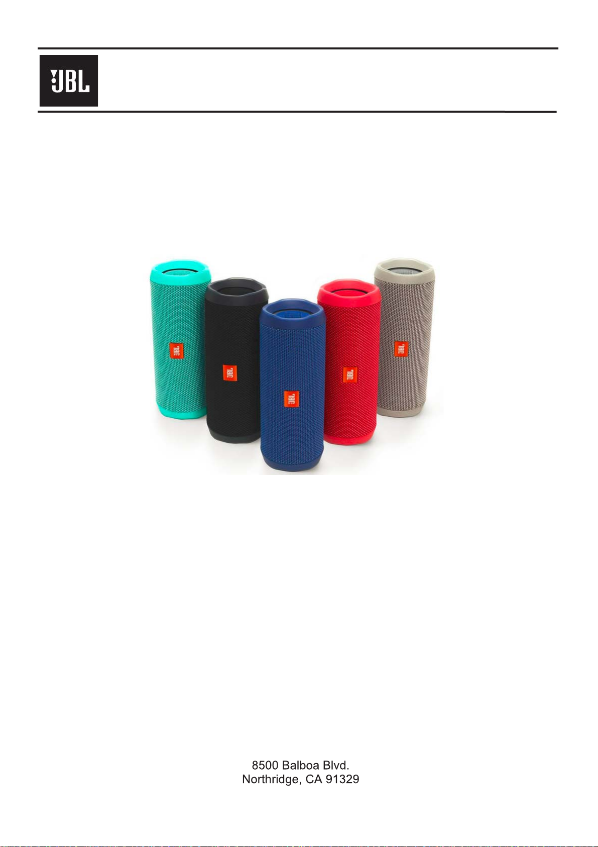
Flip 4 (S/N starting with AN)
Portable Wireless Stereo Speaker with passive bass radiators, 3000 mAh battery for 12 hours of
playing time and charging of other devices through USB, and IPX7 waterproof.
SKU: JBLFLIP4BLK , JBLFLIP4GRY, JBLFLIP4RED, JBLFLIP4BLU, JBLFLIP4TEL, JBLFLIP4WHT
JBLFLIP4BLKAM, JBLFLIP4GRYAM, JBLFLIP4REDAM, JBLFLIP4BLUAM, JBLFLIP4TELAM, JBLFLIP4WHTAM
CONTENTS
Technical Specifications
Safety Instruction, Warning & Notes
Dismantling Instruction
Set Block Diagram
Schematic & Layout Diagrams Set
Mechanical Exploded View
Packaging Exploded View
Spare Parts List
Revision List
Released by Global Quality harman/kardon, Inc.
2
3
6
13
14
28
29
30
33
Ver. 1.5 Mar. 2019
Page 2

Portable Bluetooth Speaker
Features and Benefits
Wireless Bluetooth Streaming
Wirelessly connect up to 2 smartphones or tablets to the speaker and take turns playing
impressive stereo sound.
12 hours of playtime
Built-in 3000mAh rechargeable Li-ion battery supports up to 12 hours of playtime.
IPX7 Waterproof
No more worrying about rain or spills; you can even submerge Flip 4 in water.
JBL Connect+
Link more than 100 JBL Connect+ enabled speakers together to amplify the party.
Speakerphone
Take crystal clear calls from your speaker with the touch of a button thanks to the noise
and echo-cancelling speakerphone.
Voice Assistant Integration
Access Siri or Google Now from your JBL speaker with a simple button press.
Lifestyle Material
The durable fabric material and rugged rubber housing allows your speaker to outlast
all of your adventures.
JBL Bass Radiator
Hear the bass, feel the bass, see the bass. Dual external passive radiators demonstrate
just how powerful your speaker is.
What’s in the box:
1 x JBL Flip 4
1 x JBL Micro USB Cable
1 x Safety Sheet
1 x Quick Start Guide
Warranty Card
Technical specifications:
Bluetooth version: 4.2
Support: A2DP V1.3, AVRCP V1.6, HFP V1.6,
HSP V1.2
Transducer: 2 x 40mm
Output power: 2 x 8W
Frequency response: 70Hz – 20kHz
Signal-to-noise ratio: ≥80dB
Battery type: Lithium-ion polymer
(3.7V, 3000mAh)
Battery charge time: 3.5 hours @ 5V1A
Music playing time: up to 12 hours (varies by
volume level and audio content)
Bluetooth transmitter power: 0 – 9dBm
Bluetooth transmitter frequency range:
2.402 – 2.480GHz
Bluetooth transmitter modulation: GFSK,
π/4-DQPSK, 8DPSK
Dimensions (H x W x D): 68 x 175 x 70 (mm)
Weight: 515g
HARMAN International Industries, Incorporated
8500 Balboa Boulevard, Northridge, CA 91329 USA
www.jbl.com
© 2017 HARMAN International Industries, Incorporated. All rights reserved. JBL is a trademark of HARMAN
International Industries, Incorporated, registered in the United States and/or other countries. The Bluetooth
mark and logos are registered trademarks owned by Bluetooth SIG, Inc. and any use of such marks by HARMAN
International Industries, Incorporated is under license. Other trademarks and trade names are those of their
respective owners. Features, specifications and appearance are subject to change without notice.
®
word
Page 3
Important Safety Instructions
3
harman/kardon
1. Read these instructions.
2. Keep these instructions.
3. Heed all warnings.
4. Follow all instructions.
5. Do not use this apparatus near water.
6. Clean only with a dry cloth.
7. Do not block any ventilation openings.Install in accordance with the manufacturer’s instructions.
8. Do not install near any heat sources such as radiators, heat registers, stoves or other apparatus (including
amplifiers) that produce heat.
9. Do not defeat the safety purpose of the polarized or grounding-type plug. A polarized plug has two blades with one
wider than the other. A grounding-type plug has two blades and a third grounding prong. The wide blade or the
third prong is provided for your safety. If the provided plug does not fit into your outlet, consult an electrician for
replacement of the obsolete outlet.
10. Protect the power cord from being walked on or pinched, particularly at plugs, convenience receptacles and the
point where they exit from the apparatus.
11. Only use attachments/accessories specified by the manufacturer.
12. Use only with the cart, stand, tripod, bracket or table specified by the manufacturer or sold with the
apparatus. When a cart is used, use caution when moving the cart/apparatus combination to avoid
injury from tip-over.
13. Unplug this apparatus during lightning storms or when unused for long periods of time.
14. Refer all servicing to qualified service personnel. Servicing is required when the apparatus has been damaged
in any way, such as power supply cord or plug is damaged, liquid has been spilled or objects have fallen into the
apparatus, or the apparatus has been exposed to rain or moisture, does not operate normally or has been dropped.
15. Do not expose this apparatus to dripping or splashing and ensure that no objects filled with liquids, such as vases,
are placed on the apparatus.
16. To completely disconnect this apparatus from the AC Mains, disconnect the power supply cord plug from the AC
receptacle.
17. The mains plug of the power supply cord shall remain readily operable.
18. Do not expose batteries to excessive heat such as sunshine, fire or the like.
For Products That Transmit and
Receive RF Energy:
FCC Regulations (USA Only)
FCC Information For Users
This device complies with Part 15 of the FCC Rules. Operation
is subject to the following two conditions: (1) This device
may not cause harmful interference; and (2) this device must
accept any interference received, including interference that
may cause undesired operation.
Radio and Television Interference
This equipment has been tested and found to comply with
the limits for a Class B digital device, pursuant to Part 15
of the FCC Rules. These limits are designed to provide
reasonable protection against harmful interference in a
residential installation. This equipment generates, uses and
can radiate radio frequency energy and, if not installed and
used in accordance with the instructions, may cause harmful
interference to radio communications. However, there is no
guarantee that interference will not occur in a particular
installation. If this equipment does cause interference to radio
or television reception, which can be determined by turning
the equipment off and then on, the user is encouraged to try
to correct the interference by one or more of the following
measures:
• Increase the separation between the equipment and
receiver.
• Connect the equipment to a different outlet so that the
equipment and receiver are on different branch circuits.
• Consult the dealer or an experienced radio/TV technician
for help.
NOTE: Changes or modifications not expressly approved
by Harman could void the user’s authority to operate the
equipment.
For Canadian Model
This Class B digital apparatus complies with Canadian
ICES-003.
Modèle pour les Canadien
Cet appareil numérique de la classe B est conforme à la
norme NMB-003 du Canada.
For Products with Radio Receivers
That Can Use an External Antenna:
CATV or Antenna Grounding
If an outside antenna or cable system is connected to this
product, be certain that it is grounded so as to provide some
protection against voltage surges and static charges. Section
810 of the National Electrical Code, ANSI/NFPA No. 70-1984,
provides information with respect to proper grounding of the
mast and supporting structure, grounding of the lead-in wire
to an antenna discharge unit, size of grounding conductors,
location of antenna discharge unit, connection to grounding
electrodes and requirements of the grounding electrode.
Note to CATV System Installer:
This reminder is provided to call the CATV (cable TV) system
installer’s attention to article 820-40 of the NEC, which
provides guidelines for proper grounding and, in particular,
specifies that the cable ground shall be connected to the
grounding system of the building, as close to the point of
cable entry as possible.
For CD/DVD/Blu-ray Disc™ Players:
IC Statement and Warning (Canada Only)
This Class B digital apparatus complies with Canadian ICES-
003. Cet appareil numérique de la classe B est conforme à la
norme NMB-003 du Canada.
2 of 86
CAUTION
RISK OF ELECTRIC SHOCK. DO NOT OPEN.
THE LIGHTNING FLASH WITH AN ARROWHEAD SYMBOL,
WITHIN AN EQUILATERAL TRIANGLE, IS INTENDED TO
ALERT THE USER TO THE PRESENCE OF UNINSULATED
“DANGEROUS VOLTAGE” WITHIN THE PRODUCT’S
ENCLOSURE THAT MAY BE OF SUFFICIENT MAGNITUDE TO
CONSTITUTE A RISK OF ELECTRIC SHOCK TO PERSONS.
THE EXCLAMATION POINT WITHIN AN EQUILATERAL
TRIANGLE IS INTENDED TO ALERT THE USER TO
THE PRESENCE OF IMPORTANT OPERATING AND
MAINTENANCE (SERVICING) INSTRUCTIONS IN THE
LITERATURE ACCOMPANYING THE PRODUCT.
WARNING: TO REDUCE THE RISK OF FIRE OR ELECTRIC
SHOCK, DO NOT EXPOSE THIS APPARATUS TO RAIN OR
MOISTURE.
Caution:
This product uses a laser system. To prevent direct exposure
to the laser beam, do not open the cabinet enclosure or defeat
any of the safety mechanisms provided for your protection.
DO NOT STARE INTO THE LASER BEAM. To ensure proper use
of this product, please read the owner’s manual carefully and
retain it for future use. Should the unit require maintenance
or repair, please contact your local Harman Kardon service
center. Refer servicing to qualified personnel only.
For Products That Include Batteries:
Instructions for Users on Removal and Disposal of
Used Batteries.
CAUTION
Risk of explosion if battery is incorrectly replaced.
Replace only with the same or equivalent type.
Alkaline batteries are considered nonhazardous.
Rechargeable batteries (i.e., nickel cadmium, nickel metalhydride, lithium and lithium-ion) are considered hazardous
household materials and may pose an unnecessary health
and safety risk.
In the European Union and other locations, it is illegal to
dispose of any battery with household trash. All batteries
must be disposed of in an environmentally sound manner.
Contact your local waste management officials for information
regarding the environmentally sound collection, recycling and
disposal of used batteries.
To remove the batteries from your equipment or remote
control, reverse the procedure described for inserting
batteries in the owner’s manual.
For products with a built-in battery that lasts for the lifetime of
the product, removal may not be possible for the user. In this
case, recycling or recovery centers handle the dismantling of
the product and the removal of the battery. If, for any reason, it
becomes necessary to replace such a battery, this procedure
must be performed by authorized service centers.
Page 4
4
Some semiconductor (solid state) devices can be damaged easily by static electricity. Such components commonly are called
Electrostatically Sensitive (ES) Devices. Examples of typical ES devices are integrated circuits and some field effect transistors and
semiconductor "chip" components.
The following techniques should be used to help reduce the incidence of component damage caused by static electricity.
1. Immediately before handling any semiconductor component or semiconductor-equipped assembly, drain off any electrostatic charge on
your body by touching a known earth ground. Alternatively, obtain and wear a commercially available discharging wrist strap device,
which should be removed for potential shock reasons prior to applying power to the unit under test.
2. After removing an electrical assembly equipped with ES devices, place the assembly on a conductive surface such as aluminum foil, to
prevent electrostatic charge build-up or exposure of the assembly .
3. Use only a grounded-tip soldering iron to solder or unsolder ES devices.
4. Use only an anti-static solder removal device. Some solder removal devices not classified as "anti-static" can generate electrical charges
sufficient to damage ES devices.
5. Do not use freon-propelled chemicals. These can generate electrical change sufficient to damage ES devices.
6. Do not remove a replacement ES device from its protective package until immediately before you are ready to install it. (Most replacement
ES devices are packaged with leads electrically shorted together by conductive foam, aluminum foil or comparable conductive material.)
7. Immediately before removing the protective material from the leads of a replacement ES device, touch the protective material to the
chassis or circuit assembly into which the device will be installed.
CAUTION :
8. Minimize bodily motions when handling unpackaged replacement ES devices. (Otherwise harmless motion such as the brushing together
or your clothes fabric or the lifting of your foot from a carpeted floor can generate static electricity sufficient to damage an ES devices.
Be sure no power is applied to the chassis or circuit, and observe all other safety precautions.
Each precaution in this manual should be followed during servicing.
Components identified with the IEC symbol in the parts list are special significance to safety . When replacing a component identified with
, use only the replacement parts designated, or parts with the same ratings or resistance, wattage, or voltage that are designated in the
parts list in this manual. Leakage-current or resistance measurements must be made to determine that exposed parts are acceptably
insulated from the supply circuit before retuming the product to the customer.
Page 5
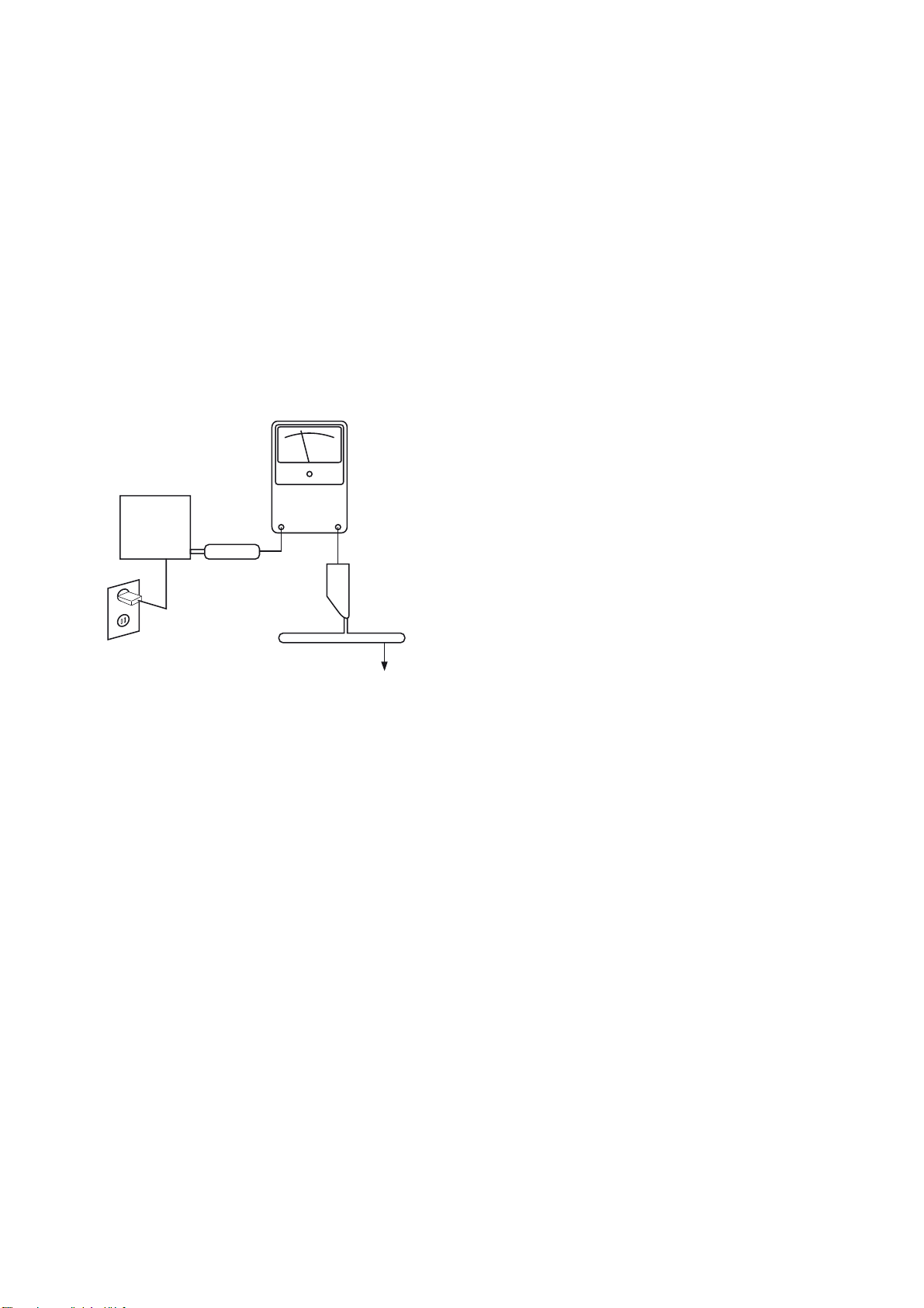
SAFETY PRECAUTIONS
The following check should be performed for the continued
protection of the customer and service technician.
LEAKAGE CURRENT CHECK
Measure leakage current to a known earth ground (water
pipe, conduit, etc.) by connecting a leakage current tester
between the earth ground and all exposed metal parts of the
appliance (input/output terminals, screwheads, metal
overlays, control shaft, etc.). Plug the AC line cord of the
appliance directly into a 120V AC 60Hz outlet and turn the
AC power switch on. Any current measured must not exceed
o.5mA.
Reading should
not be above
0.5mA
Device
under
test
Leakage
current
tester
5
Test all
exposed metal
surfaces
Also test with
plug reversed
(Using AC adapter
plug as required)
Earth
ground
AC Leakage Test
ANY MEASUREMENTS NOT WITHIN THE LIMITS
OUTLINED ABOVE ARE INDICATIVE OF A
POTENTIAL SHOCK HAZARD AND MUST BE
CORRECTED BEFORE RETURNING THE APPLIANCE
TO THE CUSTOMER.
Page 6
1 2
3 4
Disassembly Procedure
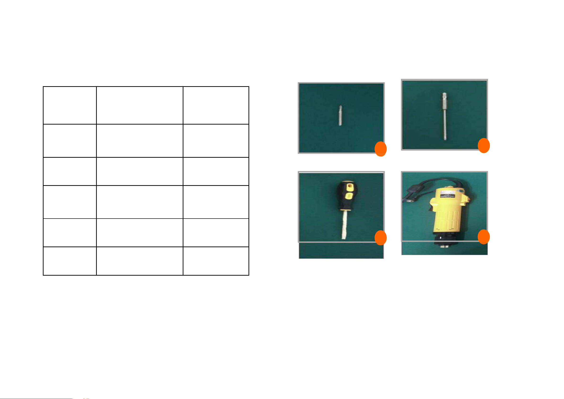
TOOL LIST
Item Description Remark
5
1
2
3 Knife
4 Electrical screw driver
5 Soldering iron
Screw driver(small)
Screw driver(middle)
2.0
3.0
II Itype
knife(wrapped
by tape)
S/N INDICATION (IF VENDOR >=2)
S/N
WITH
LABEL LOCATION ON XXXX STARTING
II
AN
II
Page 7
Dismantling Instruction Pictures
4.Take off out cabinet carefully
5. Hold on the left and right cover and
1. Open the cloth network carefully
by Knife following the direction.
2. Open the cloth network carefully
by Knife following the direction.
Note : firstly open the front cloth
network ,and then take off them.
3. Take off four screws as showed
beside left and right cover
Note : keep the waterproof and
breathable membrane intact showed
the yellow ring part
following the direction
6.Take off the 8 screws .
turn them down following the
direction ,then take out the two covers.
Page 8
Dismantling Instruction Pictures
cables
7. Disconnect two connectors by
soldering iron ,then take out the two
speakers
Take off two
8. Take off the two screws as
showed, then unplug cable on the
board ,then take out battery
9. Take off the 4pcs screws as
showed, then take out usb cover
10.Unplug the cable on the USB
oard .and then take out usb cover
b
11. Unplug 4pcs cables as
showed,and then take out main
board
12. Take off the rubber button
pad following the direction.
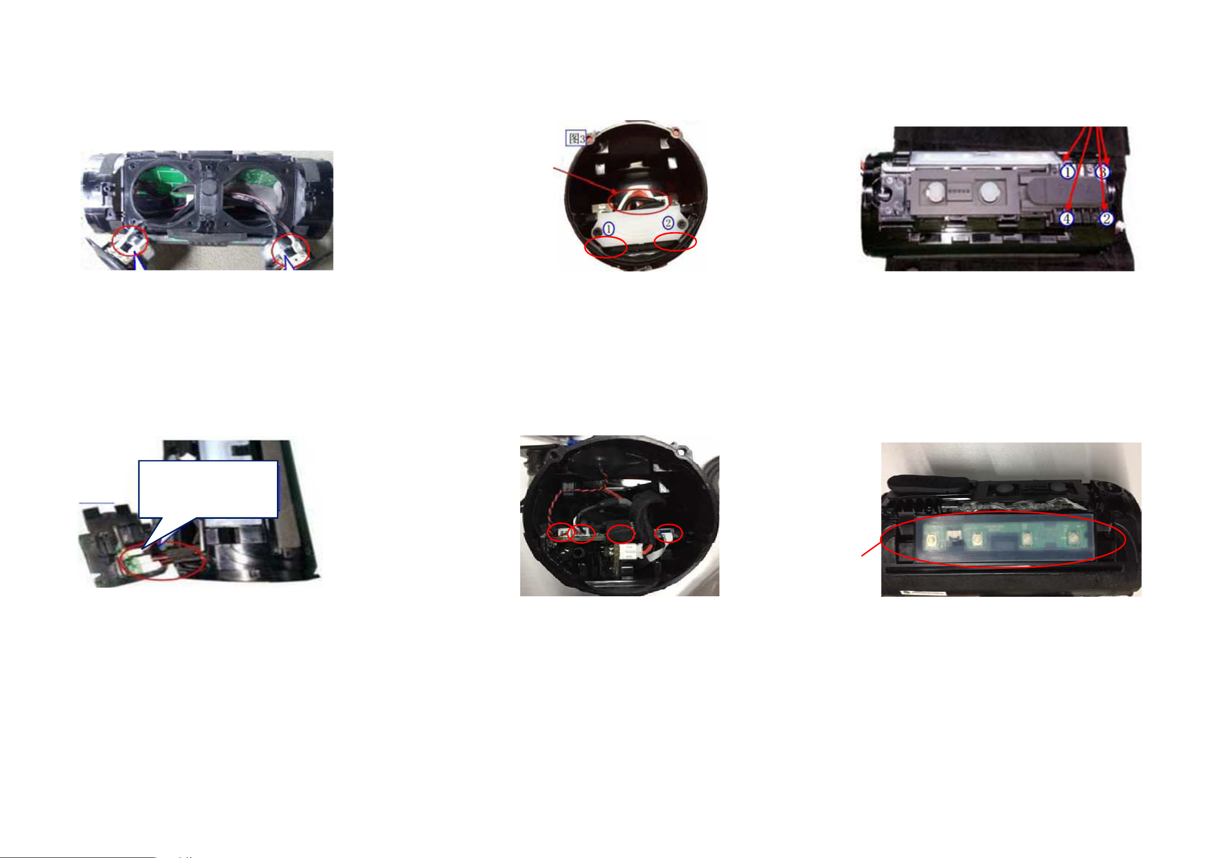
Page 9
Dismantling Instruction Pictures
Take
out KEY board
13. Take out KEY board.
14.Take off the rubber button pad
.
.
15.Unplug the FFC cable and take
Page 10
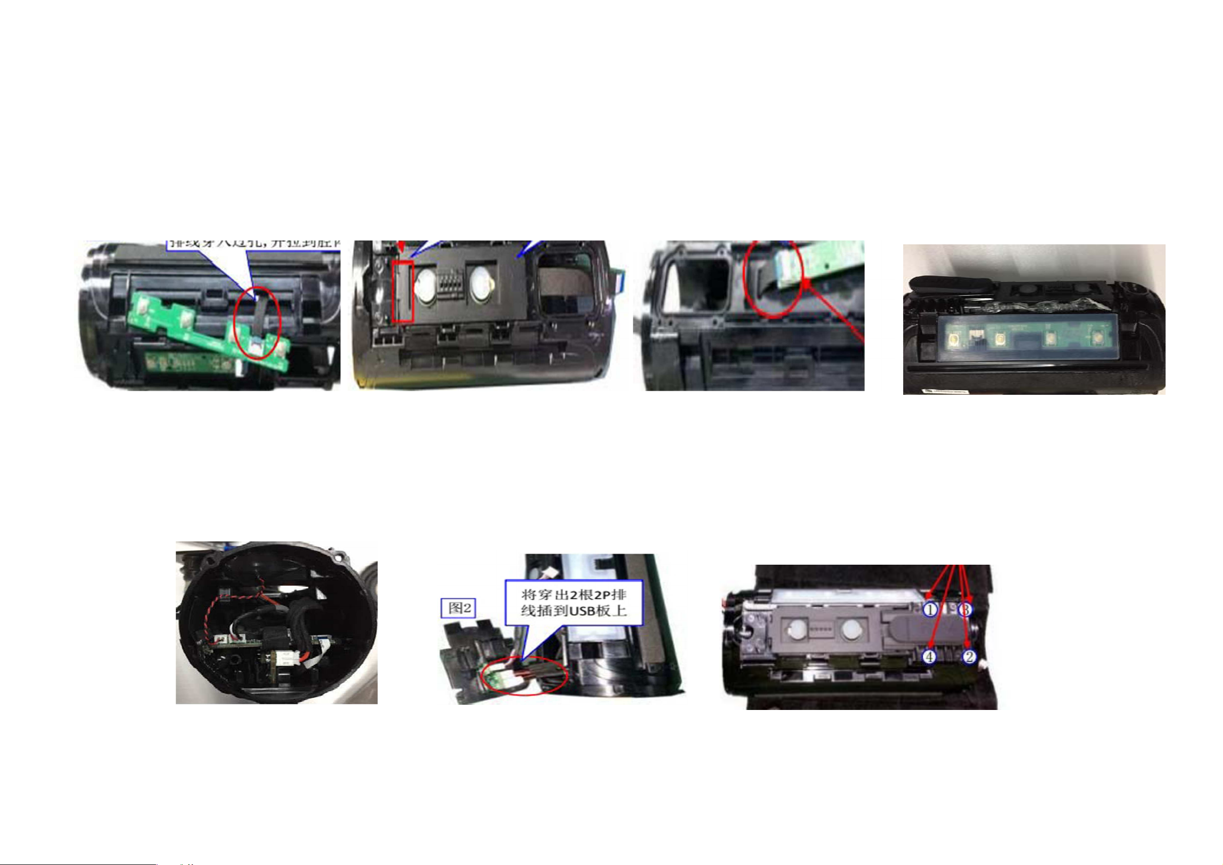
Assembly Procedure
16. Connect the FFC cable to the KEY board and LED board,then put in the cable though the hole. the board can fix the part .
17. Put the main board in the cabinet, and connect 4 cables, then connect usb board with 2 cables,and fix cover on the cabinet
by 4pcs screws.
2017-1-23 C
ONFIDENTIAL 8
Page 11

Key
Process
for
splash
-
proof
or
water
-
proof
Step16
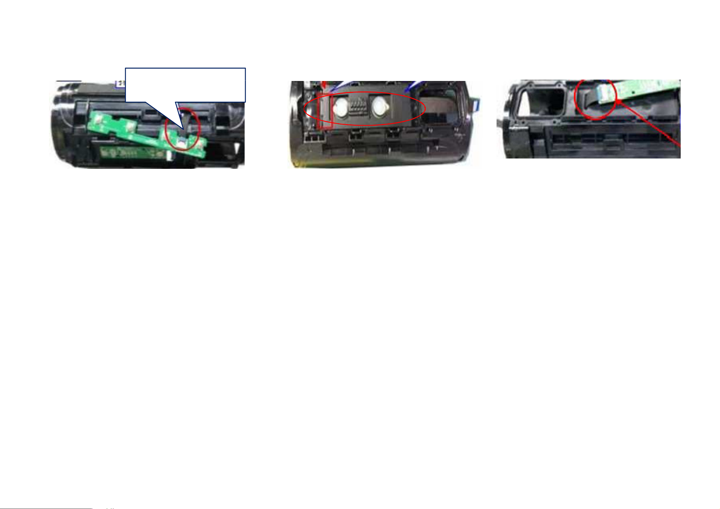
Remark
Reassembling Checkpoint
Process Step
Screws must be fixed tightly;,FFC cable must be fixed evenly and tightly
Step 17
Step 3
Screws must be fixed tightly;,FFC cable must be fixed evenly and tightly
Keep the waterproof and breathable membrane intact
2017-1-23 CONFIDENTIAL 9
Page 12

Potential
scrap
risk on materials
Material PartNumberProcess Stepp
Step1/2 Fabric grille PleaserefertotheSBOM
StStepep3/6/73/6/7
StStepep3/6/73/6/7
Step12 Keyboardrubberbuttonpad
Step14 LEDboardrubberbuttonpad
SpeakSpeakeerr
EVEVAA
Note:
1.
2.
3.
Make sure all the location where need to be fixed by screws must be even.
After reassembly, try to press one passive radiator and observe the another if it can stand up or take more than 10s to
recover flat. If yes, it should be OK if you have no special sealing equipments to test
Before test the set, the glue should be held for 4 hours for drying.
2017-1-23 CONFIDENTIAL 10
Page 13

System Block Diagram
6
Page 14

Circuit Diagram-Main Board
7-1
VCC_switch_3V3
BT_SPK_LP C700
BT_SPK_LN C701
BT_SPK_RN
BT_SPK_RP
C703
C702
5.1R704
C704
1NF
4.7UF
4.7UF
4.7UF
4.7UF
VCC_BT_OP
C765
10UF
10V
C770 /NC
R701 15K
C769 /NC
AGND
R703
C767 NC
C768 NC
BT_OP_REF
R709
22k
C766
100NF
AGND
R711
R70015K
BT_OP_REF
C713
NC
C714
NC
15K
15KR702
15k
R712 C709
15k
C710
47pF
47pF
R710
22k
C705
10UF
10V
AGND
2
A
3
VCC_BT_OP
8 4
U10B
5
B
6
BA4510 SSOP8
C706
100NF
16V
V-
V+
15k
1
15k
R707
R705
7
U10A
NJM4580V
C708
47pF
C707
47pF
R706
1k
1st_2dB
R708
1k
R723
NC
1st_2dB
R724
NC
OUT_2
R732
NC
OUT_1
R729
NC
R728
NC
DS
Q13
NC
G
C782
NC
AGND
R720
NC
NC
R721
C785
3rd_2dB
NC
R770
NC
AGND
R771
R737
NC
DS
Q16
NC
G
AGND
NC
AGND
R722
NC
DS
Q8
NC
G
R726
AGND
R727
NC
NC
2nd_2dB
R731
NC
DS
Q14
NC
R735
NC
2nd_2dB
R733
NC
C780
NC
AGND
G
C783
NC
G
C781
NC
AGND
R736
NC
C784
NC
R725
NC
DS
Q9
NC
R730
NC
3rd_2dB
R734
NC
DS
Q15
NC
G
AGND
AMP_SDZ
VCC_AMP_10V
AGND
VCC_AMP_10V
AMP_MUTE
C735
100NF
16V
R758
10K
OUT_1
AGND
AGND
2.2UF
+
C743
C736
220UF
16V
OUT_2
1
R757
100K
C740 2.2UF
AGND
20K R756
32
AGND
C742 1uF
2.2UFC744
R170
47K
Q20
MMBT3904
C741
2.2UF
R754
100K R7 39
L_in_313
AGND
GVDD
AGND
0
Mute
L705
C759220NF
1 2
R747
22
R748
22
L706
1 2
C757
220NF
25V
R744
22
R743
22
1%
C751 330PF
C752 330PF
AGND
L704
1 2
C746
330PF
C745
330PF
L703
1 2
C747
0.68UF
C753
0.68UF
25V
C754
0.68UF
25V
25V
C748
0.68UF
25V
AGND
AGND
1 2C749
1 2
C750
330pF
C755
330pF
1 2
1 2
C756
330pF
R750
3.3 OHM
R745
3.3 OHM
1%
330pF
R749
1%
R746
3.3 OHM
SPKRP
SPKRN
SPKLP
SPKLN
AGND
AGND
TP23
J3
B 3B-EH-A
TP24
TP25
J6
B 3B-EH-A
TP26
1
2
3
1
2
3
C738
C737
100NF
220UF
16V
M
SDZ
FA
RI
RI
P
L
G
VDD
G
A
GND
LINP
LINN
MUTE
AM2
AM1
AM0
SYNC
ODSE
U
N
N
IM
I
L
P
N
N/SL
AGND
L
TZ
IT
V
ThermalPad
33
AGND
AGND
1KR738
NC
U6
1
2
3
4
5
6
7
8
9
10
11
12
13
14
15
16
TPA3130D2
+
16V
PVCC
PVCC
BSPR
OUTPR
GND
OUTNR
BSNR
GND
BSPL
OUTPL
GND
OUTNL
BSNL
PVCC
PVCC
AVCC
VCC_AMP_10V
C761
220UF
+
16V
32
31
30
29
28
27
26
25
24
23
22
21
20
19
18
17
16V
C763
100NF
C739
1NF
AGND
AGND
AGND
C762
1NF
25V
C758 220NF
25V
C760
220NF
25V
Page 15

Circuit Diagram-Main Board
7-2
C
J1
GND
GND
GND
ATOM Mini RF CONN
Microphone_in
Aux_in_mic_3com1
AUX_in_mic_4Ctr
AUX_IN_L
J7
J5
B 2B-PH-K-S
J50
A1251WV-2P
1
2
TP27
3
2
1
AGND
1
2
TP28
C180
1.5NF
10V
5
TP30
TP31
4
3
2
1
RF
VCC_switch_3V3
COCOM1M1
IIIINN11
NNC1C1
AGND
L102
C181
1.5NF
10V
2
SW1
SD20
6
TP29
AGND AGND
AGND
AGND
R135
10 ohm
5%
1
VV++
NO2
NNO1O1
COM2
IIIINN22
GNGNDD
NNC2C2
7
AUX_IN_R
AGND
1%
3.24K OHM
R128
AUX_R_CH
82nHL101
82nH
AUX_L_CH
R118 1%
3.24K OHM
AGND
C129
1NF
TP33
AGND
C116
NC
R100
0 OHM
5%
C113
10NF
10V
10
9
Aux_in_mic_com 2
AUX_in_mic_Ctr
8
C130
10UF
USB_DUSB_D+
C117
NC
R112100k
VCC_BT
R147
100k
C105
1uF
6.3V
10V C120 10UF AUX_IN_R
10V C80 10UF
R72
1%
6.8K OHM
AGND
AGND
C131
47pF
USB+5V
AGND
BT_module_RF_port
VCC_switch_3V3
5%
AGND
AGND
AGND
VBAT_DCIN_DETECT 33
R113
6.8K OHM
1%
C132
47pF
L106
VBAT_DET
AGND
PWR_LED_white
BT_blue_LED
JBL_link_white_LED
GPIO8
I2C_DAT0
I2C_CLK0
AUX_IN_L
CHARGE_in_STATU(/CHG)
VBAT_DCIN_DETECT1
220R@100MHZ
C109
1uF
6.3V
AGND
BT_SPI_CLK
BT_SPI_MISO
BT_SPI_CSB
BT_SPI_MOSI
R615 15
SYS_PWR_SHUTDOWN
R141
47k
C106
10NF
10V
78
S1_DATA IN
I_MOSI
RT_RTTS
O8
SDA
25
R162
77
GND
Q18
G
32
GPIO8
1kR130
76
VDD_3V3
ME2345A
Q17
MMBT3904
GPIO21
1k
R131
74
73
GND
GPIO3375GPIO34
GPIO1529GPIO1428I2S2_DATA OUT27I2S2_DATA IN26GPIO11
DS
R142
220k
VBAT_DET
R143
100K
5%
R1083.3K
R107
Mic_BIAS_A
72
RF_IN
GPIO1630GPIO1731GPIO1832GPIO1933GPIO2034GPIO2135GND36GPIO2237GPIO2338GPIO24
AMP_MUTE
AMP_SDZ
Audio_Detect
R138
R139
66
69
68
67
70
GND71GND
SPK_RP
SPK_RN
GPIO21
AGND
SPK_LP
65
GND
SPK_LN
MIC_BIAS_A
CHG_EXT
VBAT_SENSE
VDD_MEM
VDD_PADS
I2S2_BCLK
I2S2_LRCLK
33 OHM
33 OHM
C122
10NF
10V
AGND
BT_SPK_RP
BT_SPK_RN
BT_SPK_LP
BT_SPK_LN
5%
3.3K
64
MIC_BIAS_B
MIC_LP
MIC_LN
MIC_RP
MIC_RN
GND
GPIO32
GPIO31
GPIO30
V5.0
VBAT
1V8_ OUT
GND
USB_D-
USB_D+
GND
GPIO27
GPIO26
GPIO25
39
1kR161
I2C_INT
I2C_RESET
AGND
U1
JS-BTM872H
63
62
61
60
59
58
57
56
55
54
53
52
51
50
49
48
47
46
45
44
43
42
41
40
Device_restart
HW_DET
AUX_in_mic_Ctr33 OHM
R188 10K Boost_EN
BT_VDD_MEM
AGND
Power_Off_Ready
Power_On_Off
VBAT_1 USB+5V
10K
R149
1
AIO0
2
AIO1
3
GND
4
I2S1_BCLK
5
I2S1_LRCLK
6
I2S1_ DATA OUT
7
I2
8
GND
9
SPI_CLK
10
SPI_MISO
11
SPI_CSB
12
SP
13
GND
14
RESE
UA
16
UART_CTS
17
UART_TX
18
UART_RX
19
LED0
20
LED1
21
LED2
22
GPI
23
IS2
24
I2S SCL
10V
C110
10V
C118
10UF
10UF 10
VREG_EN
I2C_DAT0
I2C_CLK0
Aux_in_mic_com 1
V
A
GND
10V
R102
C115
C11410UF
AGN
BT_VDD5
16V
AGND
R101
D
R150
22
R126
R137
10UF
BT_1V8
C107
100NF
22
AGND
Aux_in_mic_com 2
1K
R163
10 ohm
C100
1NF
USB_D-
USB_D+
33 OHM
33 OHM
R104
R145
22k
R146
33K
DC_detect
AGND
DC_detect
VCC_BT
C101
10NF
10V
I2C_DAT
I2C_CLK
4.7k R103
4.7k
AGND
C127
10NF
10V
1: GGEC 0 :TCL
HW_DET
BT_1V8 VCC_switch_3V3
USB+5V
VCC_switch_3V3
L105
1.5UH
C102
10UF
6.3V
AUX_L_CH
VCC_BT
VCC_BT
R180
100k
BT_VDD_MEM
AUX_R_CH
33
R106
R181
NC
33
R148
R184
NC
6.3V
AGND
C103
1uF
6.3V
VCC_audio_3V3
R110
2.2M
C104
R783
1uF
ESD0603V12C03
5%
AGND
VCC_audio_3V3
R153
2.2M
1
R782
ESD0603V12C03
R114
12K
1
32
AGND
32
Q10
2SC2712
Q11
2SC2712
R111
12K
MIC_BIAS_A
AGND
D750
2
1
BAT54C
Microphone_ in
R115
1k
C156
C155
10nF
10UF
25V
R120
3
150K
C133
1uF
6.3V
AGND AGND
C124
100NF
16V
R109
2.2k
AGND
1
R121
1M
AGND
Mark
VCC_BT
32
AGND
C125
15PF
25V
R123
27K
Q12
2SC2712
L103
15nH
R122
1K
TP34
C126
39PF
25V
AGND
2
1
AGND
TP47
Audio_Dete
C121
3.3NF
25V
J4
TP35
TP32
Mark
Page 16

Circuit Diagram-Main Board
4
7-3
OUT_1
OUT_2
C829 NC
C830 NC
16V
C825
4.7UF
16V
Bias1
Bias1
c828
4.7UF
16V
16V
10.0K OHM
R801
R802
10.0K OHM
1%
R805
10.0K OHM
1%
R806
10.0K OHM
1%
C826
68PF
25V
R803
10.0K OHM
1%
AGND
1%
2
-In A
-
+
B
Out B
7
1
Out A
A
V+
8
VCC_audio_3V3
U802
NJM2740
AGND
c827
100NF
16V
3
4
V-
+In A
+
-
-In B6+In B
5
R804
10.0K OHM
1%
c805
68PF
25V
AGND
U803
NJM2740
Bias1
Bias1
c806
4.7UF
16V
c807
4.7UF
16V
R807
10.0K OHM
1%
3
2
4
V-
-In A
+In A
-
+
+
B
-
-In B
Out B
+In B
7
6
5
R808
10.0K OHM
1%
D801
1N4148WS
1
Out A
A
V+
8
D802
VCC_audio_3V3
c808
4.7UF
6.3V
AGND
c809
100NF
16V
OUT_1
OUT_2
1N4148WS
U804
NJM2740
R811
10.0K OHM
Bias1
AGND
Bias1
c810
4.7UF
6.3V
c811
4.7UF
6.3V
3
4
V-
+In A
+
-
-In B
+In B
6
5
1%
R810
10.0K OHM
1%
1
2
-In A
Out A
A
+
B
Out B
V+
7
8
D803
1N4148WS
VCC_audio_3V3
c812
4.7UF
6.3V
A
GND AGND
D804
1N4148WS
VCC_audio_3V3
c813
100NF
16V
AGND
1%
R813
100K OHM
c814
10UF
6.3V
AGND
R815
27K OHM
1%
R816
1.2k
1%
R817
1M OHM
1%
A
DC_detect
TP60
R820
VCC_slg46140
TP66
Power_On_ Off
TP68
R821
10
1%
R818
10k
PW_KEY
DC_BIAS
Power_Off_Rea dy
R830
NC
1%
AGND
AGND AGND
c815
100NF
16V
R823 33 ohm
R825 1%
R827 1k
R829 1k
R831
NC
1%
c816
1UF
6.3V
510 ohm3
1
VDD
2
GPI
GPIO
4
GPIO
5
GPIO
NC
1%
13
14
GPIO
GPIO
GPIO
GPIO
GPIO
GPIO
GND
GPIO
GPIO
7
6
U801
SLG46140
12
11
10
9
R828 33 ohm
8
R822 NC
R826 33 ohm
Device_restart
VREG_EN
POWER_ON
TP61
TP62
1.033v
R833
A
3.9k
1%
R834
10K OHM
1%
10K OHM
AGND
R835
VCC_audio_3V3
13K OHM
1%
VCC_audio_3V3
R836
1.00K OHM
1%
Bias1
R837
c819
c817
4.7UF
6.3V
c818
100NF
16V
1.00K OHM
1%
100NF
16V
c820
4.7UF
6.3V
AGND
Page 17

Circuit Diagram-Main Board
Q19
MMBT3904
AGND
Charge_in_EN
32
7-4
VCC_switch_3V3
R136
10
C135
100NF
C134 1NF
33
R609
33
R154 BT Key
R608
33
33
R607 Vol+
R606 Vol-
33
Phone Key
Link key
3rd_2dB
2nd_2dB
1st_2dB
AGND
I2C_DAT
I2C_CLK
AGND
R155
4.7K
AGND
1k
1k R602
1k
1k
1k
VCC_IO_expander_3V3
R156
4.7K
R600
R601
R603
R604
R605
AGND
C152
100NF
U2
1
/INT
2
A1
3
/RESET
4
P00
5
P01
6
P02
7
P03
8
P04
9
P05
10
P06
11
P07
12
GND
VCC
SDA
24
23
22
SCL
21
A0
20
P17
19
P16
18
P15
17
P14
16
P13
15
P12
14
P11
13
P10
AGND
C151
100NF
I2C_INT
10k R6161
I2C_RESET
red_led_battery (5-15)% 1k
white ledbattery(15-30%)
white ledbattery(30-45%)
white ledbattery(45-60%)
white ledbattery(60-75%)
white ledbattery(>75%)
BT Key
Vol-
Vol+
Phone Key
AGND
VCC_switch_3V3
Link key
PW_KEY
PWR_LED_white
BT_blue_LED
JBL_link_white_LED
white ledbattery(>75%)
white ledbattery(60-75%)
white ledbattery(45-60%)
white ledbattery(30-45%)
white ledbattery(15-30%)
red_led_battery (5-15)%
C136
1NF
VCC_IO_expander_3V3
C137
C138
1NF
1NF
C140
1NF
C141
1NF
R610
10k
C139
1NF
R611
10k
C142
1NF
R612
10k
C143
1NF
R613
10k
J10
6
5
4
3
2
1
0.5S-CX-6PWB
C144
1NF
AGND
AGND
TCA1116(PW)
TP6
TP7
TP8
TP9
TP4
C191
100NF
AGND
0.5S-CX-13PWB
J9
C145
1NF
C146
1NF
C147
1NF
C148
1NF
C149
1NF
C150
1NF
AGND
13
12
11
10
9
8
7
6
5
4
3
2
1
TP10
TP11
TP12
TP13
TP14
TP15
TP17
TP18
TP19
TP20
TP21
TP22
BT_SPI_MOSI
BT_SPI_CLK
BT_SPI_MISO
BT_SPI_CSB
AGND
VCC_BT
J2
1
2
3
4
5
6
B6B-PH-K-S
Page 18

Circuit Diagram-Main Board
7-5
charge2_sys_5V
1%
R423
1%
R424
AGND
USB+ 5V
C400
C401
100NF
J401
CONN JST B 5B-PH-K-S(lying)
C430
22UF
22UF
6.3V
6.3V
5
4
3
2
1
TP3
5.36k
NTC
15k
100 @ 100MHz
L402
C414
22UF
AGND AGNDAGND
TP1
C409
100NF
TP2
NTC
C407
22UF
10V
VBAT_1
charge_in_5V
C426
100nF
C406
22UF
charge_in_VCC
C404
AGND
R404
1K
AGND
19
MODE
20
AGND
R432
100K
VIN
21
SYS
22
SW
23
PGND
24
PGND
charge2_sys_5V
C424
C405
1uF
AGNDAGND AGND AGN DAGND
C408
1uF
1uF
22UF
C415
R407
0.02 ohm
5%
0805
charge2_sys_5V
1 2
MCW-0530-2R2-N2
L401
100nF
R414
15K
Charge_in_EN
PWIN
16
13
15
14
17
18
EN
VB
VCC
ILIM
PWIN
N/C1CHG2BOOST3CSP4BATT5AGND
TP401
6
/BOOST
AGND
VCC_switch_3V3
R172
1
10K
TMR
AGND
C410
330nF
REG
ACOK
FB
NTC
ISET
OLIM
R173
100K
32
Q21
MMBT3904
AGND
U9
MP2637
12
/ACOK
11
charge_sys_FB
10
NTC
9
8
7
R420
51k
AGND AGND
TP49
CHARGE_in_STATU(/CHG)
R439
120K OHM
1%
1%
R421
100k
TP400
USB+ 5V
charge_in_5V
1%
R400
15K
1%
R401
5.1k
AGND AGND
Q4
32
MMBT3904
1
AGND
R426
51k
R427
39.2k
AGND
R438
100k
5%
R431
100k
1%
R410
21.5K
1%
R411
5.1k
USB+ 5V
PWIN
R428
470k
5
V+
IN
+
1
AGND
AGND
V-
2
4
3
OUT
-IN
C423
100nF
USB_D-
U8
LMV331TP
R437
10k
AGND
R429
VBAT_1
C501
C503
22uF 25V
22uF 25V
AGND
NC
C502
22uF 25V
R504
R503
R502
R501
different pair
same length
AGND
0.01ohm
0.01ohm
0.01ohm
0.01ohm
R506
100K
L501
1 2
MCF-1040-1R5-N2
C507
100nF
SDR
Boost_10V
Boost_EN
3428_SW
1
2
3
4
5
6
3428_SW
21
BST
SDR
OUT
EN
MODE
SENSE
SW7SW8PGND9PGND
U7
MP9428A
Q1 MTB04N03
S
S
S
G
C504
2.2uF
C511
12
NC
8
D
7
D
6
D
5
D
AGND
AGND
C506 2.2nF
C159
1.5nF
AGND
R507
27k
R511
R513
3k
51
AGND
100uF/16V
+-20%
MP16VL100MC5R7
C508
Boost_10V
C509
+
22UF 25V
25V
R512
100k
AGND
R440
13k
R509
1%
47k
22UF
C510
VCC_AMP_10V
ME4435
Q2
1
3
Q3
AGND
4
C513
100NF
R515
1K
32
1
R514
100K
1 2
AGND
R508
100K
MMBT3904
DC_BIAS
8
7
62
5
R505
SYS_PWR_SHUTDOWN
47K
C512
10NF
TP402
R516
NC
1
2
3
4
AGND
18
SW19SW20SW
10
AGND
PGND17PGND
AGND
COMP
PGND
22
VDD
SDR
16
C505
15
SS
FB
IN
33NF
14
13
12
11
AGND
POWER_ON
R434
47k
1%
VBAT_1
1%
R435
100k
1%
R433
100k
AGND
MMBT3904
1
C402
NC
C427
100nF
Q7
AGND
MTP3401N3
32
12
SS1040(SOD-123)
D404
Q5
32
1
VBAT_1
C128
100NF
10NF
C428
10V
AGND
Q6
3 2
MTP3401N3
R436
10K
AGND
AGND
R442
4.7K
1
U3
1
IN
2
GND
3
EN
SGM2036_3.3V
AGND
OUT
BP/FB
C425
1uF
USB+ 5V
5
4
R443
10 ohm
5%
0603
C432
10NF
SS1040(SOD-123)
D403
VCC_slg46140
C431
100NF
12
100NF
C418
AGND
C419
1NF
C420
10UF
10V
R419
10K
AGND
U5
1
IN
2
GND
3
EN
SGM2036_3.3V
BP/FB
OUT
5
4
AGND
C429
10NF
VCC_switch_3V3
C403
100NF
AGND
10UF
C412
10V
TP48
10NF
10V
C123
VCC_audio_3 V3
R430
5.1
AGND
C417
100NF
Page 19

Circuit Diagram-AUX Board
7-6
J301
CK3.5-97-04
f
e
1
c
d
b
a
C803
ESD0402V18C15
C804
ESD0402V18C15
2
3
J310
Page 20

Circuit Diagram-KEY+LED Board
A K K A K A K A K A K
K K
K
7-7
R190
200 ohm
D12
K
white power
A
R189
200 ohm
D21
R193
power
AGND
R198
200
BT blue LED
D23
R194
NC
R197
200
BT blue LED
D22
NC
VCC_3V3
JBL_Link_key
R199
R200
200 ohm
JBL_Link_white LED
D24
200 ohm
D25
C192 10nF
R201
10K
TP461 TP462
Battery >75% white
A
D15
Battery 60-75% white
A
K
A
D16 D17 D18 D19 D20
Battery 15-30% white
A
A
K
A
10
11
12
13
1
2
3
4
5
6
7
8
9
J11
0.5
S-CX-13PWB
AGND
TP46
TP45
T
P44
TP43
TP42
TP41
TP40
TP39
TP36
TP38
TP37
AGND
AGND AGND AGND AGND AGND AGND
Battery 30-45% white
Battery 45-60% white
Battery <15% Red
Page 21

Circuit Diagram-KEY Board
7-8
R191
NC
BT_Key
V-
R192
NC
V+
TP51 TP54
TP52
TP53
AGND
AGND
TP55
6
5
4
3
2
1
J100
0.5S-CX-6PWB
AGND
R195
NC
phone
R196
NC
Page 22

Circuit Diagram-USB Board
3
SHIED
SHIED
SHIED
7-9
J12
1
2
UN1159C-N1211-7H -A
CON600
VBUS
1
2
D-
D+
4
ID
5
SHIED
GND
9 8 7 6
C800 C801 C802
NC
B 2B-PH-K-S
J120
1
2
A1251WV-2P
AGND
Page 23

Print-Layout-Main Board
7-10
Page 24

Print-Layout-AUX Board
7-11
Page 25

Print-Layout-KEY+LED Board
7-12
Page 26

Print-Layout-USB Board
7-13
Page 27

Print-Layout-KEY Board
7-14
Page 28

MECHANICAL EXPLODED VIEW
s2
C6
P11
P8
24
P12
S1
C2
S13
C3
C10
C3
P2
S28
s2
S20
P12
S5
S4
s2
P4
s3
P3
C9
C8
s3
P7
S27
S29
S4
C5
S6
S6
31
P10
C7
S21
S7
P6
P13
S8
C4
s2
C1
P5
P1
Pos.
No.
C1 CAS32YP337SFBLACKL PASSIVE RADIATOR BLK L FLIP4 AN 1
C1 CAS32YP339SFREDL PASSIVE RADIATOR RED L FLIP4 AN 1
C1 CAS32YP341SFBLUEL PASSIVE RADIATOR BLU L FLIP4 AN 1
C1 CAS32YP343SFGRAYL PASSIVE RADIATOR GRY L FLIP4 AN 1
C1 CAS32YP345SFTEALL PASSIVE RADIATOR TEL L FLIP4 AN 1
C1 CAS32YP347SFWHITEL PASSIVE RADIATOR WHT L FLIP4 AN 1
C2 CAS32YP338SFBLACKR PASSIVE RADIATOR BLK R FLIP4 AN 1
C2 CAS32YP340SFREDR PASSIVE RADIATOR RED R FLIP4 AN 1
C2 CAS32YP342SFBLUER PASSIVE RADIATOR BLU R FLIP4 AN 1
C2 CAS32YP344SFGRAYR PASSIVE RADIATOR GRY R FLIP4 AN 1
C2 CAS32YP346SFTEALR PASSIVE RADIATOR TEL R FLIP4 AN 1
C2 CAS32YP348SFWHITER PASSIVE RADIATOR WHT R FLIP4 AN 1
C3 CAS43FP330SHZ FULLRANGE SPEAKER FLIP4 AN 2
C4 CABGSP87269301 BATTERY 3.7V 3000MAH FLIP4 AN 1
C5 VOP12970B MAIN PCBA W/USB BOARD FLIP4 AN 1
C6 08-0FLIP4-FE0 LED/POWER KEY PCBA FLIP4 1
P1
VGP1A078R79T31W17Z WRAPPING BODY BLK FLIP4 AN (priority) 1
P1 VGP1A078R79T31W17Y WRAPPING BODY BLK FLIP4 AN (2nd choice) 1
P1 VGP1A078R80T31W17Z WRAPPING BODY GRY FLIP4 AN 1
P1 VGP1A078R81T31W17Z WRAPPING BODY RED FLIP4 AN (priority) 1
P1 VGP1A078R81T31W17Y WRAPPING BODY RED FLIP4 AN (2nd choice) 1
P1 VGP1A078R82T31W17Z WRAPPING BODY BLU FLIP4 AN 1
P1 VGP1A078R83T31W17Z WRAPPING BODY TEL FLIP4 AN 1
P1 VGP1A078R84T31W17Z WRAPPING BODY WHT FLIP4 AN 1
P4
VKH1A026R73 STRAP HOLDER BLK FLIP4 AN 1
P4 VKH1A026R74 STRAP HOLDER GRY FLIP4 AN 1
P4 VKH1A026R75 STRAP HOLDER RED FLIP4 AN 1
P4 VKH1A026R76 STRAP HOLDER BLU FLIP4 AN 1
P4 VKH1A026R77 STRAP HOLDER TEL FLIP4 AN 1
P4 VKH1A026R78 STRAP HOLDER WHT FLIP4 AN 1
P5 VGL1A350R73 INDICATOR BUTTON FLIP4 AN 1
P7 CGG1A302J27ZA FABRIC GRILL BKT ASSY BLK FLIP4 AN 1
P7 CGG1A302J28ZA FABRIC GRILL BKT ASSY GRY FLIP4 AN 1
P7 CGG1A302J29ZA FABRIC GRILL BKT ASSY RED FLIP4 AN 1
P7 CGG1A302J30ZA FABRIC GRILL BKT ASSY BLU FLIP4 AN 1
P7 CGG1A302J31ZA FABRIC GRILL BKT ASSY TEL FLIP4 AN 1
P7 CGG1A302J32ZA FABRIC GRILL BKT ASSY WHT FLIP4 AN 1
P8 CKK1A042T32 USB COVER BLK FLIP4 AN 1
P8 CKK1A042T33 USB COVER GRY FLIP4 AN 1
P8 CKK1A042T34 USB COVER RED FLIP4 AN 1
P8 CKK1A042T35 USB COVER BLU FLIP4 AN 1
P8 CKK1A042T36 USB COVER TEL FLIP4 AN 1
P8 CKK1A042T37 USB COVER WHT FLIP4 AN 1
P9 CDV1A019T32 USB BRACKET GASKET FLIP4 AN 1
REBBUR BCP YEK83T120A1VDC01P
P11
08-FLP4K1-PW1 RUBBER POWER KEY FLIP4 1
egasU noitpircseDN/P
1NA 4PILF ABCP YEKDMSB17921PIV7C
1NA/LT 4PILF DRAOB BSU0NI-MN4PLF-808C
1NA/LT 4PILF DRAOB XUA0UA-MN4PLF-809C
1NA 4PILF Y'SSA CIMCIM4PILFXJC01C
1NA 4PILF GNISUOH NIAM66R180A1PGV2P
1NA 4PILF TEKCARB BSU66R720A1HKV3P
1NA 4PILF REVOC YRETTAB76R280A1PGV6P
1
1NA 4PILF KLB PARTSLKB4PILF010A1ZDC31P
1NA 4PILF YRG PARTSYRG4PILF110A1ZDC31P
1NA 4PILF DER PARTSDER4PILF210A1ZDC31P
1NA 4PILF ULB PARTSELB4PILF310A1ZDC31P
1NA 4PILF LET PARTSLET4PILF410A1ZDC31P
1NA 4PILF THW PARTSTHW4PILF510A1ZDC31P
Page 29

Packaging Exploded View
5.Specification box
8.Paper plate(bottom)
9
2.USB cable box
1.USB cable
6.Gift box
7.Gift box bag
4.
Specification bag
3.Specifcation
9.Paper plate(top)
Page 30

JBL FLIP4 AN SPARE PARTS LIST
Pos. No. P/N Description Usage
C1 CAS32YP337SFBLACKL PASSIVE RADIATOR BLK L FLIP4 AN 1
C1 CAS32YP339SFREDL PASSIVE RADIATOR RED L FLIP4 AN 1
C1 CAS32YP341SFBLUEL PASSIVE RADIATOR BLU L FLIP4 AN 1
C1 CAS32YP343SFGRAYL PASSIVE RADIATOR GRY L FLIP4 AN 1
C1 CAS32YP345SFTEALL PASSIVE RADIATOR TEL L FLIP4 AN 1
C1 CAS32YP347SFWHITEL PASSIVE RADIATOR WHT L FLIP4 AN 1
C2 CAS32YP338SFBLACKR PASSIVE RADIATOR BLK R FLIP4 AN 1
C2 CAS32YP340SFREDR PASSIVE RADIATOR RED R FLIP4 AN 1
C2 CAS32YP342SFBLUER PASSIVE RADIATOR BLU R FLIP4 AN 1
C2 CAS32YP344SFGRAYR PASSIVE RADIATOR GRY R FLIP4 AN 1
C2 CAS32YP346SFTEALR PASSIVE RADIATOR TEL R FLIP4 AN 1
C2 CAS32YP348SFWHITER PASSIVE RADIATOR WHT R FLIP4 AN 1
C3 CAS43FP330SHZ FULLRANGE SPEAKER FLIP4 AN 2
C4 CABGSP87269301 BATTERY 3.7V 3000MAH FLIP4 AN 1
C5 VOP12970B MAIN PCBA W/USB BOARD FLIP4 AN 1
C6 08-0FLIP4-FE0 LED/POWER KEY PCBA FLIP4 1
C7 VIP12971BSMD KEY PCBA FLIP4 AN 1
C8 08-FLP4NM-IN0 USB BOARD FLIP4 TL/AN 1
C9 08-FLP4NM-AU0 AUX BOARD FLIP4 TL/AN 1
C10 CJXFLIP4MIC MIC ASS'Y (IPX7 WATERPROOF) FLIP4 AN 1
P1 VGP1A078R79T31W17Z WRAPPING BODY BLK FLIP4 AN (priority) 1
P1 VGP1A078R79T31W17Y WRAPPING BODY BLK FLIP4 AN (2nd choice) 1
P1 VGP1A078R80T31W17Z WRAPPING BODY GRY FLIP4 AN 1
P1 VGP1A078R81T31W17Z WRAPPING BODY RED FLIP4 AN (priority) 1
P1 VGP1A078R81T31W17Y WRAPPING BODY RED FLIP4 AN (2nd choice) 1
P1 VGP1A078R82T31W17Z WRAPPING BODY BLU FLIP4 AN 1
P1 VGP1A078R83T31W17Z WRAPPING BODY TEL FLIP4 AN 1
P1 VGP1A078R84T31W17Z WRAPPING BODY WHT FLIP4 AN 1
P2 VGP1A081R66 MAIN HOUSING FLIP4 AN 1
P3 VKH1A027R66 USB BRACKET FLIP4 AN 1
P4 VKH1A026R73 STRAP HOLDER BLK FLIP4 AN 1
P4 VKH1A026R74 STRAP HOLDER GRY FLIP4 AN 1
P4 VKH1A026R75 STRAP HOLDER RED FLIP4 AN 1
P4 VKH1A026R76 STRAP HOLDER BLU FLIP4 AN 1
P4 VKH1A026R77 STRAP HOLDER TEL FLIP4 AN 1
P4 VKH1A026R78 STRAP HOLDER WHT FLIP4 AN 1
P5 VGL1A350R73 INDICATOR BUTTON FLIP4 AN 1
P6 VGP1A082R67 BATTERY COVER FLIP4 AN 1
P7 CGG1A302J27ZA FABRIC GRILL BKT ASSY BLK FLIP4 AN 1
P7 CGG1A302J28ZA FABRIC GRILL BKT ASSY GRY FLIP4 AN 1
P7 CGG1A302J29ZA FABRIC GRILL BKT ASSY RED FLIP4 AN 1
P7 CGG1A302J30ZA FABRIC GRILL BKT ASSY BLU FLIP4 AN 1
P7 CGG1A302J31ZA FABRIC GRILL BKT ASSY TEL FLIP4 AN 1
P7 CGG1A302J32ZA FABRIC GRILL BKT ASSY WHT FLIP4 AN 1
P8 CKK1A042T32 USB COVER BLK FLIP4 AN 1
P8 CKK1A042T33 USB COVER GRY FLIP4 AN 1
P8 CKK1A042T34 USB COVER RED FLIP4 AN 1
P8 CKK1A042T35 USB COVER BLU FLIP4 AN 1
P8 CKK1A042T36 USB COVER TEL FLIP4 AN 1
P8 CKK1A042T37 USB COVER WHT FLIP4 AN 1
P9 CDV1A019T32 USB BRACKET GASKET FLIP4 AN 1
Page 31

P10 CDV1A021T38 KEY PCB RUBBER AN 1
P11 08-FLP4K1-PW1 RUBBER POWER KEY FLIP4 TL 1
P13 CDZ1A010FLIP4BKL STRAP BLK FLIP4 AN 1
P13 CDZ1A011FLIP4GRY STRAP GRY FLIP4 AN 1
P13 CDZ1A012FLIP4RED STRAP RED FLIP4 AN 1
P13 CDZ1A013FLIP4BLE STRAP BLU FLIP4 AN 1
P13 CDZ1A014FLIP4TEL STRAP TEL FLIP4 AN 1
P13 CDZ1A015FLIP4WHT STRAP WHT FLIP4 AN 1
CWC4G1A06G110B05J0 FFC CABLE (06P, 0.5MM ,110MM) FLIP4 AN 1
CJJ2D050ZD JACK STEREO (3.5MM BLACK) FLIP4 AN 1
CJJ9X037Z JACK MICRO USB B FLIP4 AN 1
CLZ9Z120Z ESD SUPPRESSOR (0R2 0.2PF/12V) FLIP4 AN 1
CLZ9Z280Z ESD SUPPRESSOR (3PF/18V 1608) FLIP4 AN 1
CNVBM875HF3 BT MODULE 4.2 FLIP4 AN 1
CSA3A068Z ANT BT (2.4GHZ FPCB L=40MM ) FLIP4 AN 1
CST1A051ZT SW TACT (H=1.5MM 250GF) FLIP4 AN 1
CVDLTSTC193TBKT5A LED BLUE 1608 FLIP4 AN 1
CVDLTSTC281KRKT LED RED 1005 FLIP4 AN 1
CVDLTWC193TS5L LED WHITE 1608 FLIP4 AN 1
CVDLTWC281DS5 LED WHITE 1005 FLIP4 AN 1
U8 CVILMV331TPTR IC SINGLE COMPARTATOR FLIP4 AN 1
U9 CVIMP2637GRZ IC BATTERY CHARGER FLIP4 AN 1
U7 CVIMP9428AGLZ IC BOOST CONVERTER FLIP4 AN 1
SW1 CVISD20TR IC ANALOG DUAL SWITCH FLIP4 AN 1
U3,U5 CVISD6211TR IC REGULATOR(+3.3V 5P) FLIP4 AN 1
U801 CVISLG4V4826V IC SYSTEM LOGIC 14P FLIP4 AN 1
U2 CVITCA1116PWR IC I/O EXPANDER 24P FLIP4 AN 1
U10,U802,
U803,U804
U6 CVITPA3130D2DAPR IC D-AMP(2X15W/8R 32P) FLIP4 AN 1
CVITP2412TSR IC DUAL AUDIO OPAMP FLIP4 AN 1
CVT2SC2712GRFSBR TR 2SC2712 NPN SOT-23 FSBR FLIP4 AN 1
CWB1D002140AO001 WIRE ASS'Y (2P #22 140MM B/R) FLIP4 AN 1
CWB2A002140AP001 WIRE ASS'Y (2P #28 140MM B/R) FLIP4 AN 1
CWBFLIP4J3 WIRE ASS'Y (3P #22 90MM R/W/B) FLIP4 AN 1
CWBFLIP4J310 WIRE ASS'Y (3P #28 80MM R/W/B) FLIP4 AN 1
CJS9W021Z USB A TO MICRO B CABLE 1.0M FLIP4 AN 1
CPG1A1143UA GIFT BOX ASSY WHT FLIP4 AN (priority) 1
CPG1A1143VA GIFT BOX ASSY TEL FLIP4 AN (priority) 1
CPG1A1143WA GIFT BOX ASSY BLU FLIP4 AN (priority) 1
CPG1A1143XA GIFT BOX ASSY RED FLIP4 AN (priority) 1
CPG1A1143YA GIFT BOX ASSY GRY FLIP4 AN (priority) 1
CPG1A1143ZA GIFT BOX ASSY BLK FLIP4 AN (priority) 1
CPG1A1143Z GIFT BOX FLIP4BLK AN (2nd choice) 1
CPG1A1143U GIFT BOX FLIP4WHT AN (2nd choice) 1
CPG1A1143V GIFT BOX FLIP4TEL AN (2nd choice) 1
CPG1A1143W GIFT BOX FLIP4BLU AN (2nd choice) 1
CPG1A1143X GIFT BOX FLIP4RED AN (2nd choice) 1
CPG1A1143Y GIFT BOX FLIP4GRY AN (2nd choice) 1
VPG1A1143AC GIFT BOX FLIP4BLK AN (3rd choice) 1
VPG1A1143AH GIFT BOX FLIP4WHT AN (3rd choice) 1
VPG1A1143AG GIFT BOX FLIP4TEL AN (3rd choice) 1
VPG1A1143AD GIFT BOX FLIP4BLU AN (3rd choice) 1
VPG1A1143AE GIFT BOX FLIP4RED AN (3rd choice) 1
Page 32

VPG1A1143AF GIFT BOX FLIP4GRY AN (3rd choice) 1
CPN1A042 CORRUGATED BOARD FLIP4 AN 1
Page 33

Version 1.5
* Some P/N and Pos. No. and Description on Exploded View corrected, add Pos. # 10 KEY PCB RUBBER.
2019-03
 Loading...