

Page 1
harman consumer group
SERVICE CENTER TRAINING GUIDE
Servicing Class D Amplifiers
And The Theory of Operation
Page 2
Introduction to Class D Amplifiers
Page 2
Harman Consumer Group 250 Crossways Park Dr. Woodbury, New York 11797
Email [email protected] Web www.harmanservice.com
I. A Brief Description of Other Audio Amplifier Classes
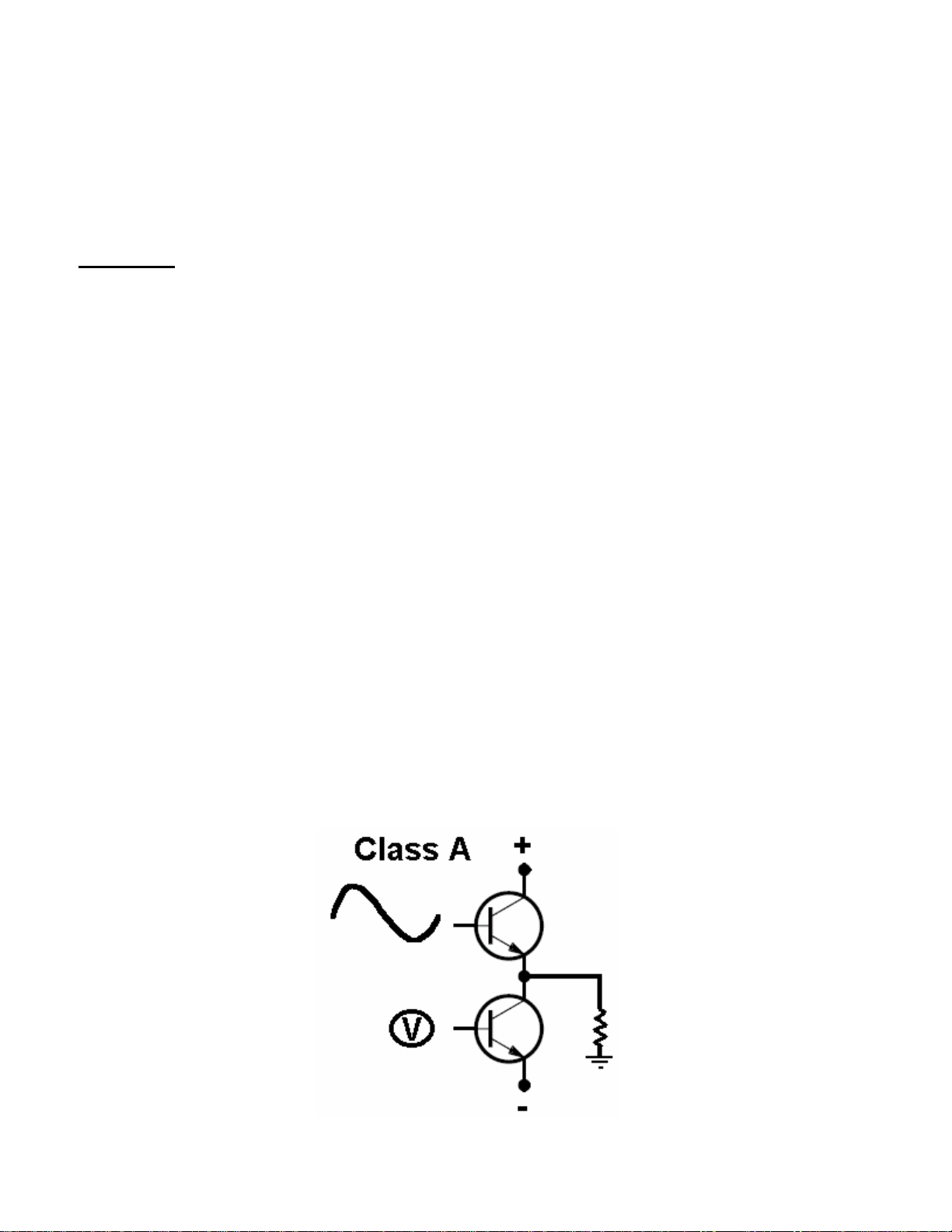
Class A
• Class A amplifiers are biased. The signal operates in the linear
region between cutoff and saturation.
• The output devices conduct continuously, the bias current
flows in the output devices at all times.
• In Class A operation, both devices are always on. There is
never a time when one output or another is turned off.
• Class A is the most inefficient of all power amplifier designs.
• Class A amplifiers are large, very heavy and run very hot. All
of this is due to the amplifier constantly operating at full power.
• Class A designs are the most linear, with the least amount of
distortion.
Page 3
I. A Brief Description of Other Audio Amplifier Classes (cont’d.)
Page 3
Harman Consumer Group 250 Crossways Park Dr. Woodbury, New York 11797
Email [email protected] Web www.harmanservice.com
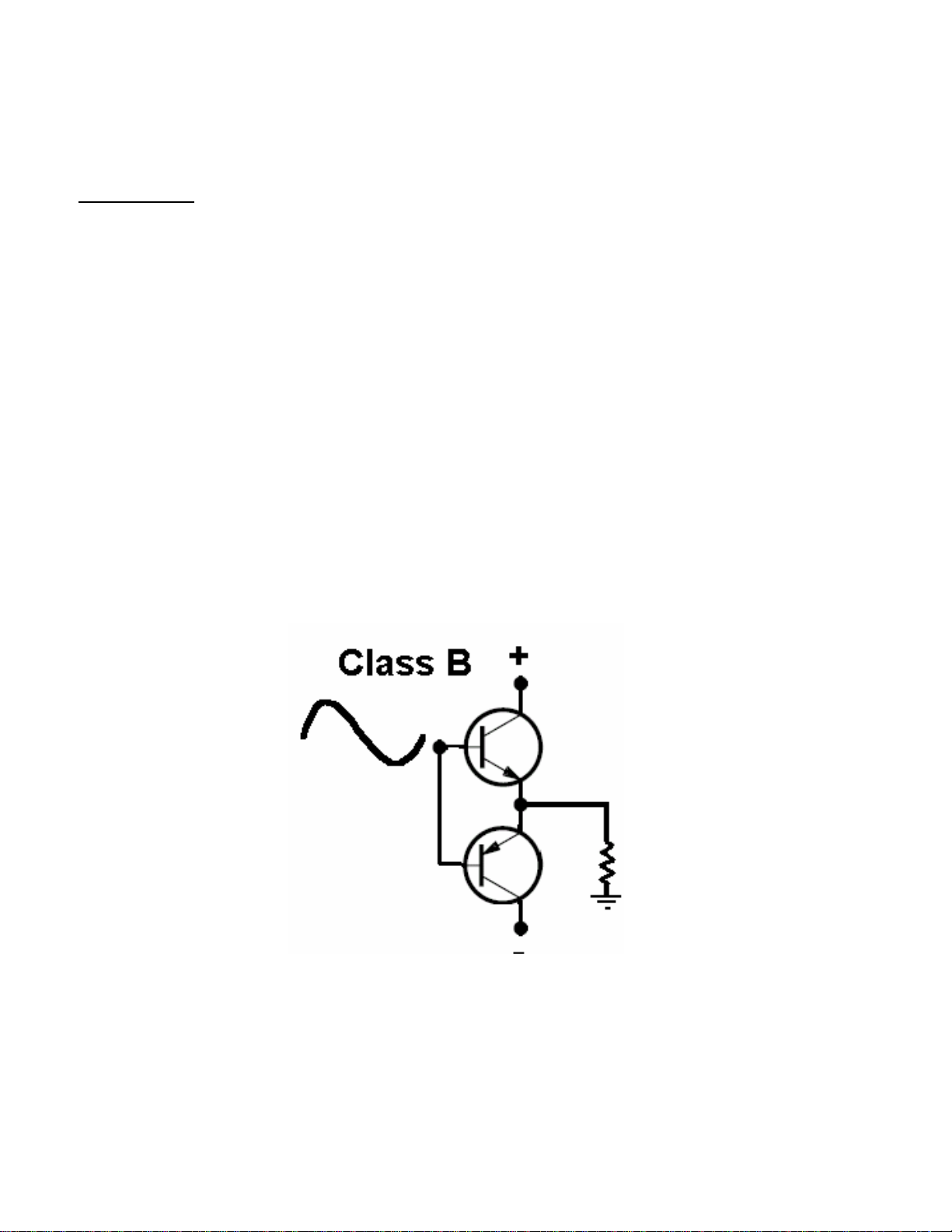
Class B
• Class B operation is the opposite of Class A. Both
output devices are never allowed to be on at the same
time.
• The output devices have no bias (.6 volts is needed to
bias each device).
• Each output device is on for exactly one half of the time.
Class B designs have high efficiency but poor linearity;
this is due to extreme crossover distortion.
Page 4
I. A Brief Description of Other Audio Amplifier Classes (cont’d.)
Page 4
Harman Consumer Group 250 Crossways Park Dr. Woodbury, New York 11797
Email [email protected] Web www.harmanservice.com
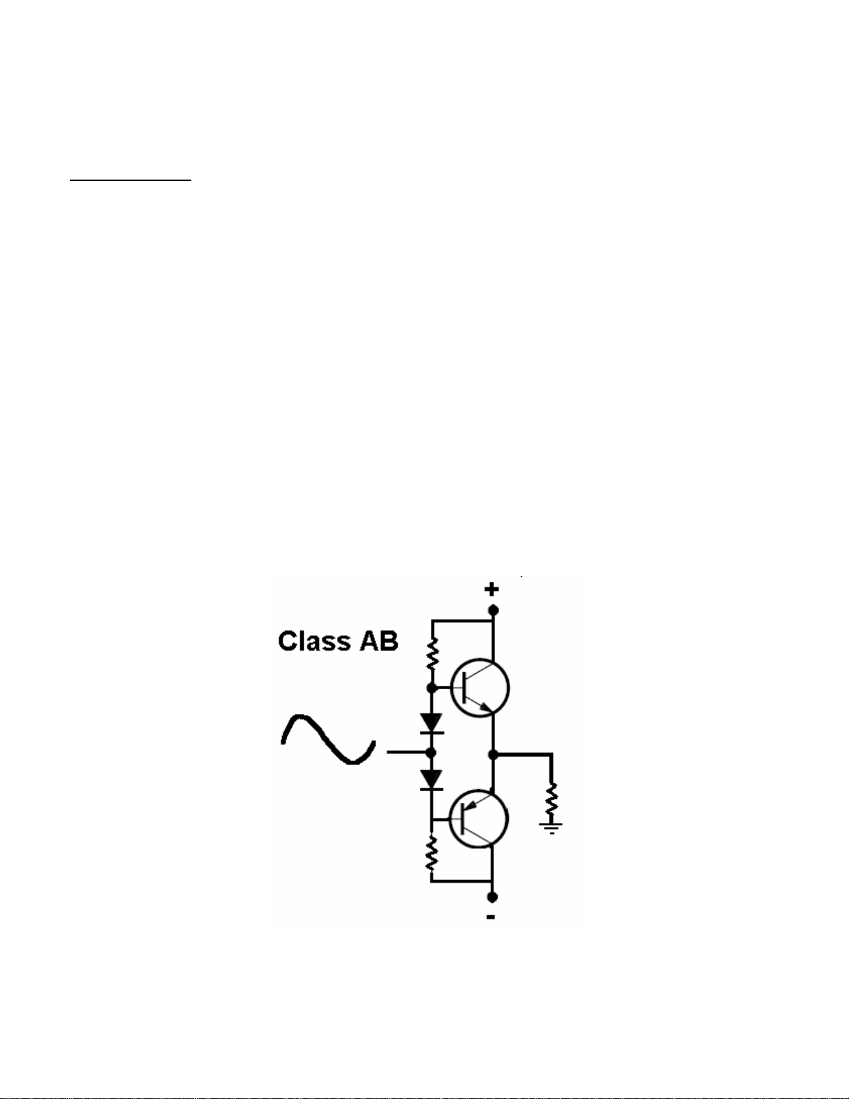
Class A/B
• Class A/B is a combination of Class A and Class B.
• Class A/B operation allows both devices to be on at the
same time that the outputs have a bias voltage, so
current flows to the output devices more than half of the
time but less than the full time of the output wave form.
This is called bias, and bias eliminates extreme crossover
distortion.
Page 5
I. A Brief Description of Other Audio Amplifier Classes (cont’d.)
Page 5
Harman Consumer Group 250 Crossways Park Dr. Woodbury, New York 11797
Email [email protected] Web www.harmanservice.com
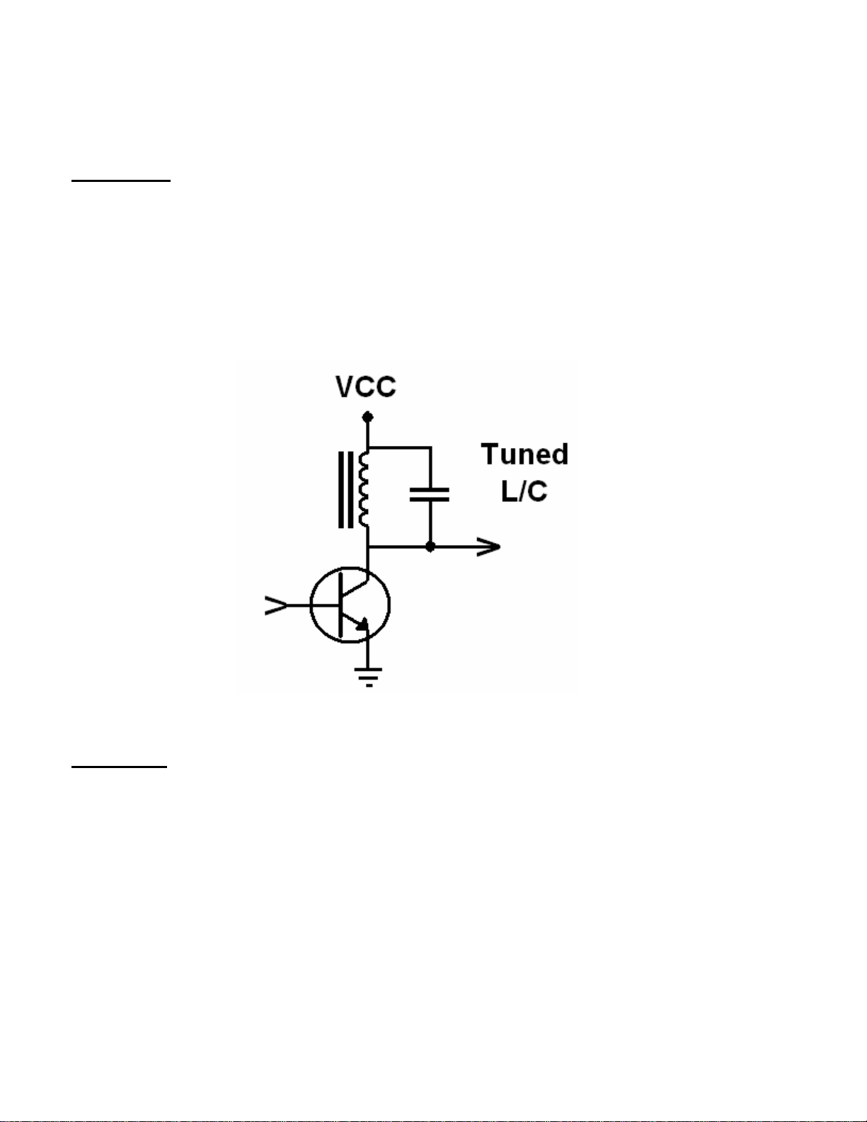
Class C
Class C is used in single frequency RF applications.
(Radio)
Class F
There are no existing products that use this class of
amplifier. (You could be the first!)
Page 6
Page 6
Harman Consumer Group 250 Crossways Park Dr. Woodbury, New York 11797
Email [email protected] Web www.harmanservice.com
I. A Brief Description of Other Audio Amplifier Classes (cont’d.)
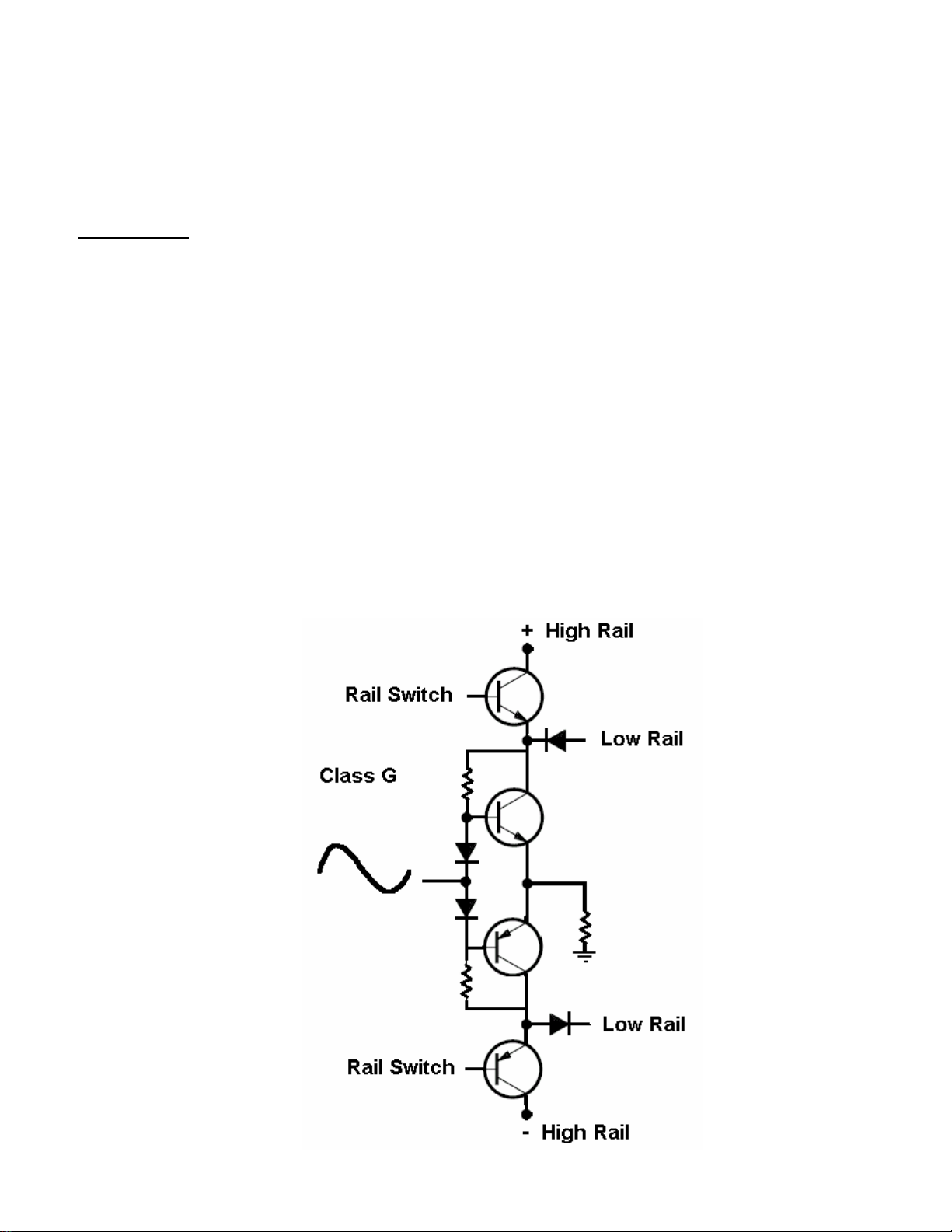
Class G
In Class G operation two power supplies’ voltages are
used. A Class A/B amp is connected to a low voltage rail
and a diode transistor matrix. When the signal is greater
than the lower voltage rail can supply, a transistor switch
connects the output stage to a higher voltage rail. This
involves changing the power supply voltage from a lower
level to a higher level automatically when a larger output
swing is required for large signal peaks.
Page 7
I. A Brief Description of Other Audio Amplifier Classes (cont’d.)
Page 7
Harman Consumer Group 250 Crossways Park Dr. Woodbury, New York 11797
Email [email protected] Web www.harmanservice.com
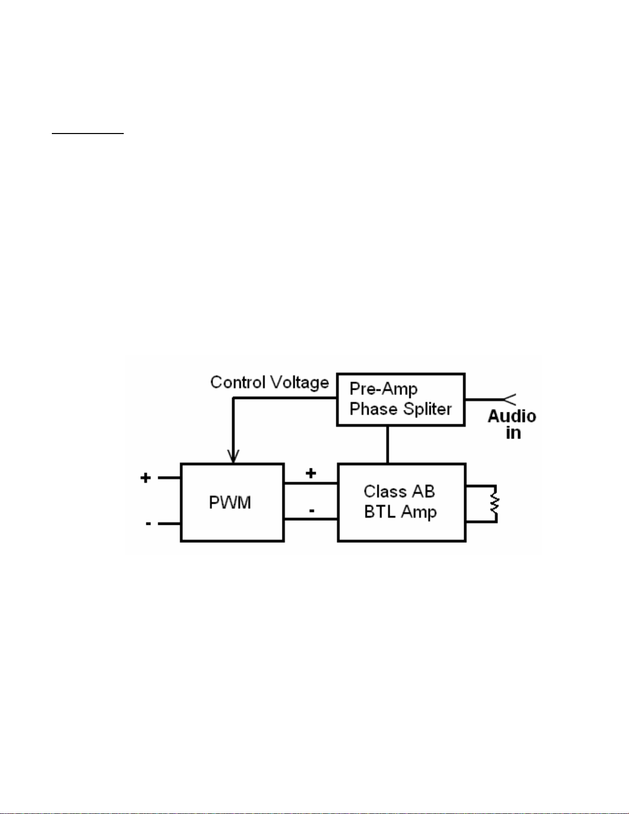
Class H
The Class H design is like the Class G, except that the
power supply tracks the audio input signal. This is the
same as in the Bash power amps that we use in our
amplifiers.
Page 8
II. What Is Class D Amplification?
Page 8
Harman Consumer Group 250 Crossways Park Dr. Woodbury, New York 11797
Email [email protected] Web www.harmanservice.com
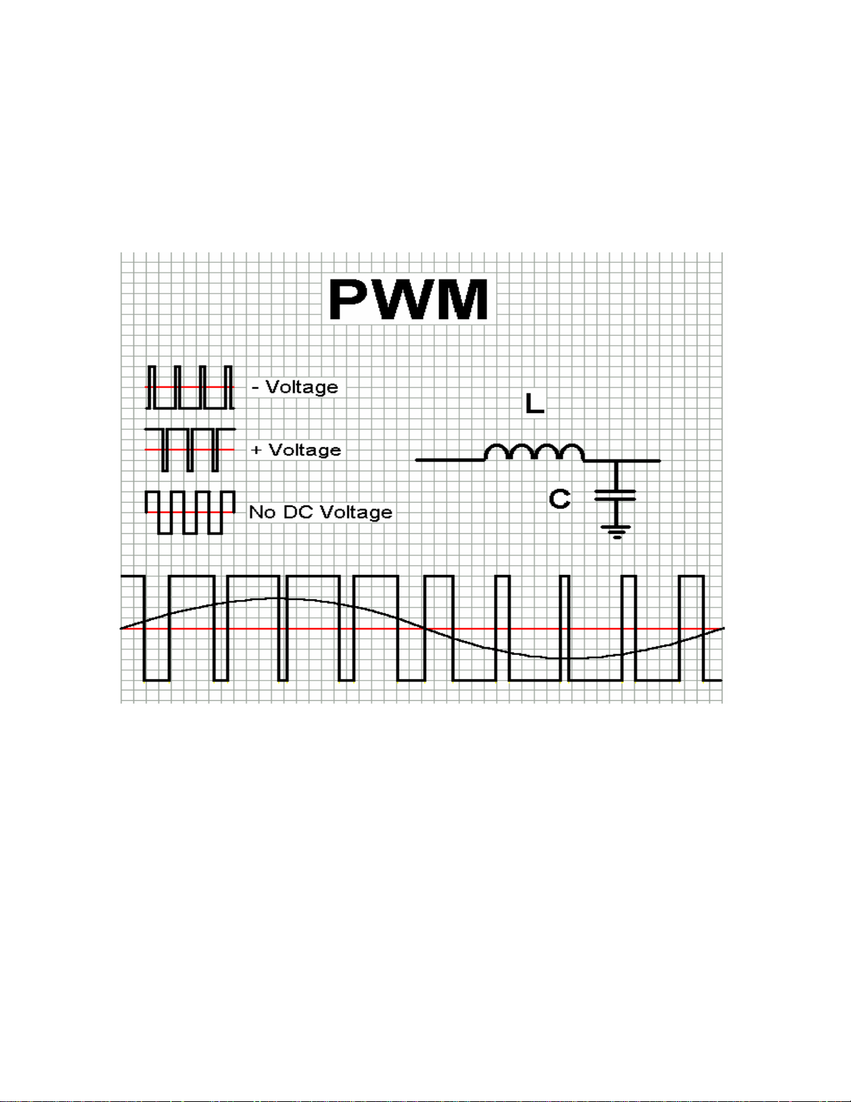
It’s a switched mode amplifier using “Pulse Width
Modulation,” or, PWM.
The output signal is proportional to the ratio of positive and
negative of the square wave. Then it is filtered by a low pass
filter to remove the high frequency content of
the square wave. If the duty cycle is 50% no output from the LC
filter will be produced.
If the positive portion of the square is greater than 50% then the
output will be a positive voltage from the LC network.
If you modulate the square wave the output will vary
proportionally to the modulated signal.
Page 9
Page 9
Harman Consumer Group 250 Crossways Park Dr. Woodbury, New York 11797
Email [email protected] Web www.harmanservice.com
II. What Is Class D Amplification? (cont’d.)
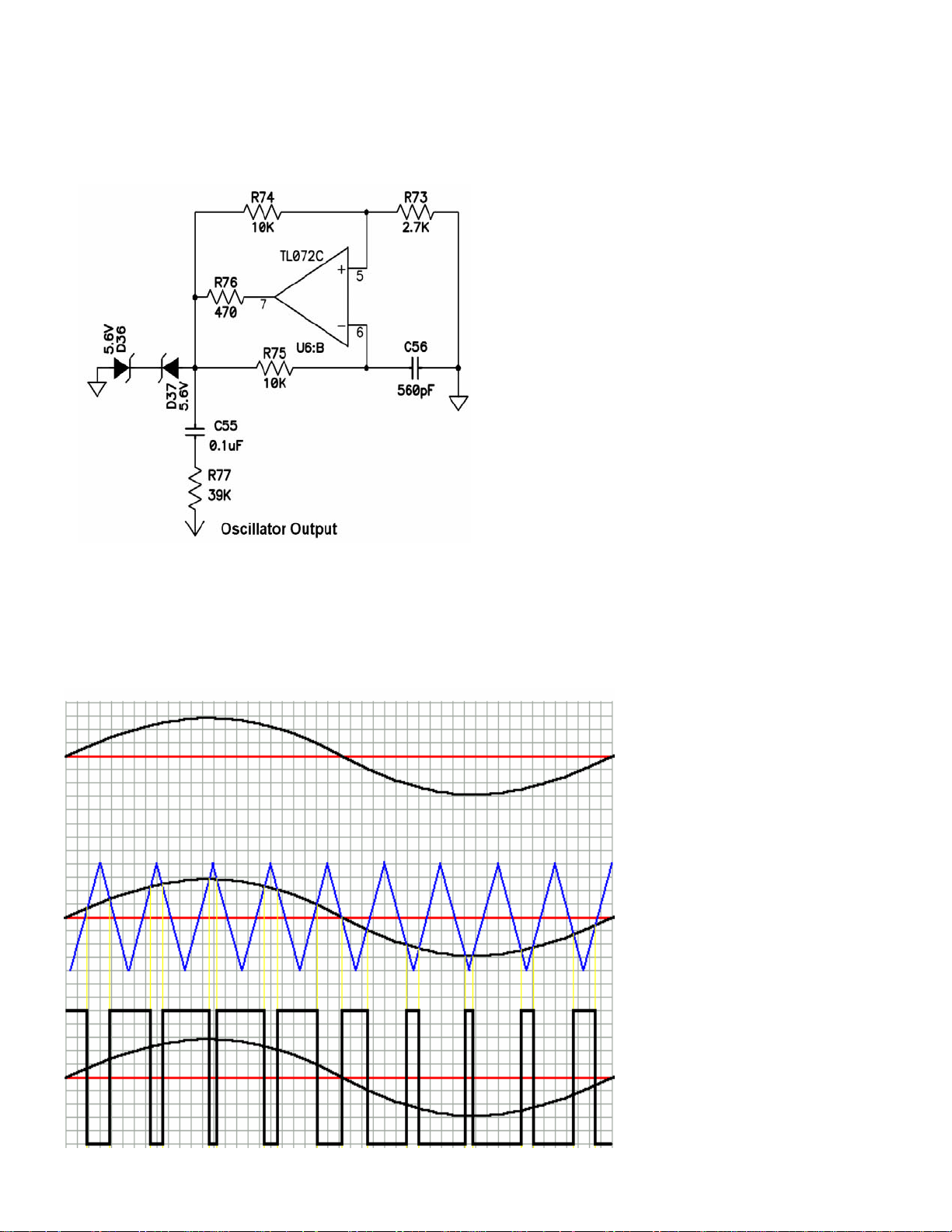
oscillator to the input
The output of the
of the opamp U6:A is
a ramp waveform.
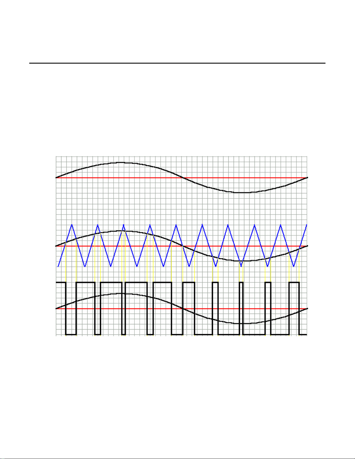
The input signal is modulated with a much higher fixed frequency. The
waveform of the fixed frequency is a saw-tooth signal formed from the
100khz ramp generator.
Fig. A
Fig. B
Fig. C
Page 10

Page 10
Harman Consumer Group 250 Crossways Park Dr. Woodbury, New York 11797
Email [email protected] Web www.harmanservice.com
II. What Is Class D Amplification? (cont’d.)
Class D Modulation is obtained by using an opamp as a
summer to achieve PWM.
On our Class D Amps
the oscillator, feedback and audio all
feed into one input of the opamp.
The result is a summation of all the
signals at pin 2 of IC U6 with a
result of a square wave out at pin 1
of U6.
Note: The opamps gain is very high
due to 2.2meg feedback resistor R50.
Page 11

II. What Is Class D Amplification? (cont’d.)
Page 11
Harman Consumer Group 250 Crossways Park Dr. Woodbury, New York 11797
Email [email protected] Web www.harmanservice.com
Feedback
Purpose:
• To compensate for nonlinearities either in the amplifier stage or the
load with the end purpose of reducing distortion.
• We use two feedback paths for our design; the main one is before the
output inductor (L3 on most amps). It consists of a low pass filter to
remove the carrier and reconstruct the modulated audio signal. This
signal is fed to amplifier U6.
• The second feedback path we will call the AC sine sense, and it’s
taken after the low pass filter. This is a minor feedback and is used for
additional stability.
Page 12

II. What Is Class D Amplification? (cont’d.)
Page 12
Harman Consumer Group 250 Crossways Park Dr. Woodbury, New York 11797
Email [email protected] Web www.harmanservice.com
+15VSW is
referenced
from –V,
not ground
Always check the
+/-15 Volt supply. It is the
supply for all of the opamps.
VCC of U7 (IR2111) is delayed at turn on (mute release). U7 is the drive
that insures that the mosfets never turn on at the same time.
Page 13

II. What Is Class D Amplification? (cont’d.)
Page 13
Harman Consumer Group 250 Crossways Park Dr. Woodbury, New York 11797
Email [email protected] Web www.harmanservice.com
Protect
only
triggers mute
Base of Q10 goes low. Voltage at Q10 goes up, turning on Q7.
This then puts the amp in mute.
Remember!
Protection is only
MUTE (standby mode).
Page 14

Page 14
Harman Consumer Group 250 Crossways Park Dr. Woodbury, New York 11797
Email [email protected] Web www.harmanservice.com
II. What Is Class D Amplification? (cont’d.)
BTL Class D
Opamp
A
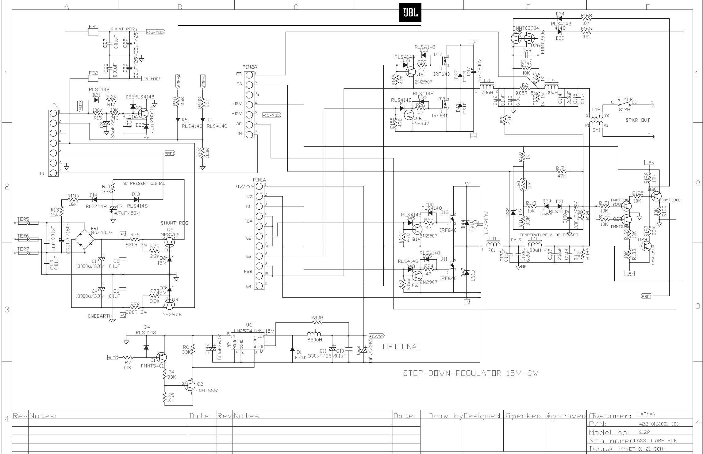
This is the output block of the JBL S120PII. All that was
added to the amp was a second FET output stage and
opamp A. Opamp A has no gain, and is used for phase
nd
inversion of the audio to the 2
FET output stage.
When servicing this amp, please remember that the
speaker out +/- is hot to ground.
Never ground the S-.
Page 15

II. What Is Class D Amplification? (cont’d.)
Page 15
Harman Consumer Group 250 Crossways Park Dr. Woodbury, New York 11797
Email [email protected] Web www.harmanservice.com
Class D Power Amp Harman/Kardon HKTS 10/20
The HKTS10/20 is different from other Class D amps because it
uses discrete components for the FET drivers and the output
FETs themselves.
The drivers and outputs are Class B amps. They are used to
insure that the mosfets never turn on at the same time.
The mosfets are IRF640 and IRF9640. They are built with
Schottky diodes inside the FETs. The amps contain inductors
(low pass filters) and drive loads with
will clamp fly-back voltages and clamp waveforms that have
inductance. The diodes
overshoot.
Page 16

Page 16
Harman Consumer Group 250 Crossways Park Dr. Woodbury, New York 11797
Email [email protected] Web www.harmanservice.com
Service Bulletin JBL2003-06 - April 2003 This is considered a Minor repair
To: All JBL Service Centers
Model: S120PII
Subject: Distortion When Coming Out Of Standby
In the event you receive an S120PII subwoofer with the complaint “There is a brief chirping sound, or
short oscillation that occurs when the unit is in the AUTO mode, in Standby, when it’s triggered ON
with a music signal”, follow the procedure below to correct this condition:
Synopsis: Replace D60 (RLS4148 diode) with a 3.6V Zener Diode; add new Resistor.
1) Remove the amplifier assembly from the subwoofer cabinet (12 Phillips screws).
2) Remove the Plastic Amp Cover from the faceplate (4 Phillips screws).
3) The area of concern is on the Class D Driver PCB (Small Upright PCB on the MAIN AMP PCB). A
long, thin, soldering iron tip is recommended. Care must be taken not to damage surrounding
components, like large inductor pair L8.
4) Locate, remove D60 (RLS4148 diode); replace with a 3.6V zener diode, JBL Part# ZMM5227BCT-ND.
When replacing D60 the polarity of the new (zener) diode should be reversed
5) Add new 27KΩ resistor, JBL Part# 299-27K, to the indicated connections. (This component,
electrically, will be in parallel with R37, reducing its value to <22KΩ). Assure the leads do not come
into contact with any other connections; insulate the leads if necessary.
6) Replace amp cover and return amplifer assembly to cabinet.
7) Test the subwoofer to assure the distortion is no longer present.
Service Bulletin
.
Page 17

Page 17
Troubleshooting tips and solutions to common service problems
For models: PS-10, PS-12, SUB750 TIP# INFTT2003-04
Subject: Replacing MOSFETS Q18, Q22
In the event you need to replace MOSFET transistors Q18 or Q22 as part of a repair, it is important to use
ONLY the Infinity part# FE106401110 or only the brands: International Rectifier, or Fairchild.
Replace both Q18 and Q22 MOSFET’s in the circuit, even if only one seems to be damaged.
Do NOT mix & match these components from different manufacturers, or batches. They should be
identical.
TECH TIPS
Harman Consumer Group 250 Crossways Park Dr. Woodbury, New York 11797
Email [email protected] Web www.harmanservice.com
Page 18

E250P
Page 18
Harman Consumer Group 250 Crossways Park Dr. Woodbury, New York 11797
Email [email protected] Web www.harmanservice.com
DETAILED TROUBLESHOOTING
A. Power Amp Section
Resistance
Check
Resistance from S+ (SPK O/P) to GND should be >1M Ω (NO LOAD)
Resistance from V+ (C6 P+) to V- (C8 P-) gradually Fully CHARGED should read >10k Ω
Resistance from V+ (C6 P+) to S+ (SPK O/P) should read >1MΩ
Resistance from V- (C8 P-) to S+ (SPK O/P) should read >1M Ω
2. Power Up LED RED
With a 5mV signal to Low level input, LED should change to GREEN
-Voltage measurements (DVM)
OP AMP
LED
P-U4(1) P-U4(7)
RED 0Vrms 11.84VDC
GREEN 7.13Vrms -12.93VDC
3. D.C. Operation
-Voltage measurements (DVM) on CLASS D POWER AMP
Between V+ Q4(E) Q1(C)
And This
Point
Get this
Reading
GND V- GND GND GND GND GND GND GND GND
71.7V 0V -71.7V 0V -71.7V -71.5V -71.2V 0V 0V 4.65V
Q10(C)
U7(1) U7(2) U7(4) U7(6) U7(7) U7(8)
4. Check Switching Frequency
• Oscilloscope - USE THE PROBE TIP TO U6(7) TO GND
• Reading 100kHz +/-10%,24Vp-p
B. Pre Amp Section
Line Level Input Sensitivity
-Set up Turn level, X’OVER FREQ POT Fully CW and LFE switch off
Generator Set at 200mV@50Hz
Signal to Line level input
Page 19
E250P
Page 19
Harman Consumer Group 250 Crossways Park Dr. Woodbury, New York 11797
Email [email protected] Web www.harmanservice.com
DETAILED TROUBLESHOOTING (CONT'D)
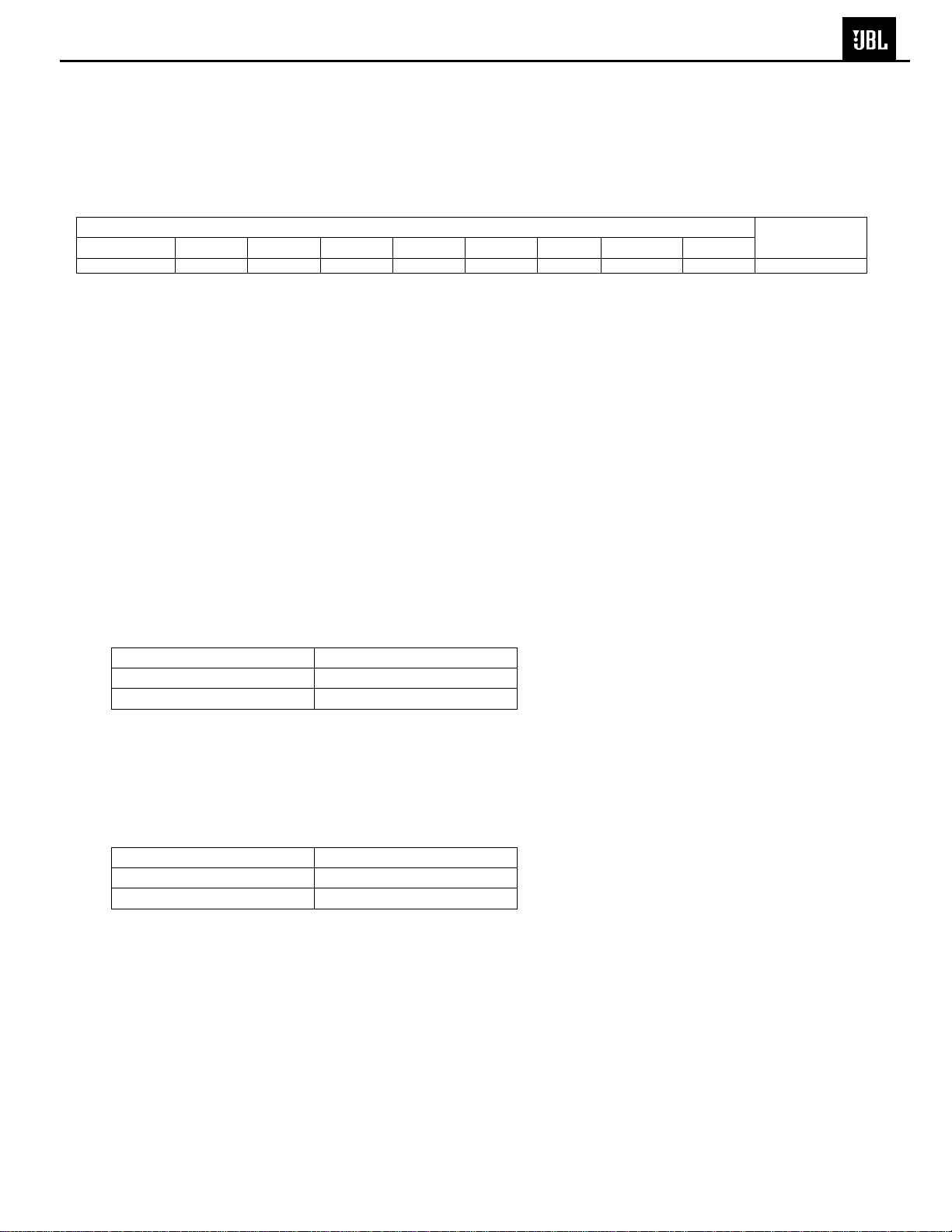
- Voltage measurements
OP AMP
U2(1) U2(14) U2(8) U3(7) U3(1) U3(14) U3(8) U5(7) U5(1)
306.9mV 461mV 460mV 658mV 628mV 598mV 2.326V 2.02V 3.57V 23.33V
2. High Level Input Sensitivity
-Set up Turn level, X’OVER FREQ POT Fully CW and LFE switch off
Set Generator at 1.3V@50Hz
Signal to High level input
-Voltage measurements 15.3V at speaker output
3. Low-Pass
-Set up Set Generator at 200 mV@100Hz
Signal to
Measure voltage at S+ speaker output
-Voltage measurement
X’OVER FREQ. Setting Output
CW 14.03V
CCW 4.8V
Line level input
SPEAKER
O/P
4. LFE
-Set up Set Generator at 200mV@200Hz
Signal to
Measure voltage at S+ speaker output
LFE switch Setting Output
Normal 6V
LFE 18.32V
See flow chart next page for diagnostics.
Line level input
Page 20

,
E250P
Page 20
Harman Consumer Group 250 Crossways Park Dr. Woodbury, New York 11797
Email [email protected] Web www.harmanservice.com
DETAILED TROUBLESHOOTING (CONT'D)
FLOW CHART
TO GROUND. ALL TEST INSTRUMENTS CONNECTED TO THE OUTPUT MUST
BE FLOATING. ATTACH THE SCOPE PROBE TIP TO S - and REFERENCE
LEAD TO S+.
(A 10mV signal may need from the input to trigger the Switch turn on)
START
Resistance check
(no load)
between V+ V-,
V+ O/P,V- O/P
and O/P to GND
is > 10K
no
no
OK
yes
yes
Power up with no
signal input
LED RED
CAUTION : SPEAKER OUTPUT IS FLOATING AND IS NOT PROTECTED AGAINST A SHORT
Check +/-15V-MOD
+/-15V voltage at
U 6(8),U6(4)
Check
FB1,FB2,C45,
Replace
Q18,Q22
OK
I/P:10mv/50HZ
Check +15V/SW
Q4(E) TO V-
C50,C60,C63,
R81,R82
no
no
OK
yes
yes
Check Q4(E)
TO V-
= 0V D.C.
no
no
OK
yes
yes
Use scope to check
switching
frequency U6(7)
100KHz
+/-10% , ~24Vp-p
no
no
OK
yes
yes
CLASS D AMP OK
Discharge C37,
Check fuse
transformer, L4,
rectifier, C6 and C8
Check
MUTE(+8V) and
Q24,Q25,Q26
OK
Check
U7(1) = -58.3V
OK
Use scope to
check O/P U7(6)
and GND
143Vp-p square
wave shown
OK
Check
L2,L3,C71,C72,
C73
C74
Check
MUTE(-12.9V),
And
Q24,Q25,Q26
Check
U7,Q16,Q17,
Q20,Q21,R87,
D26,D35,C64
Page 21

E250P
Page 21
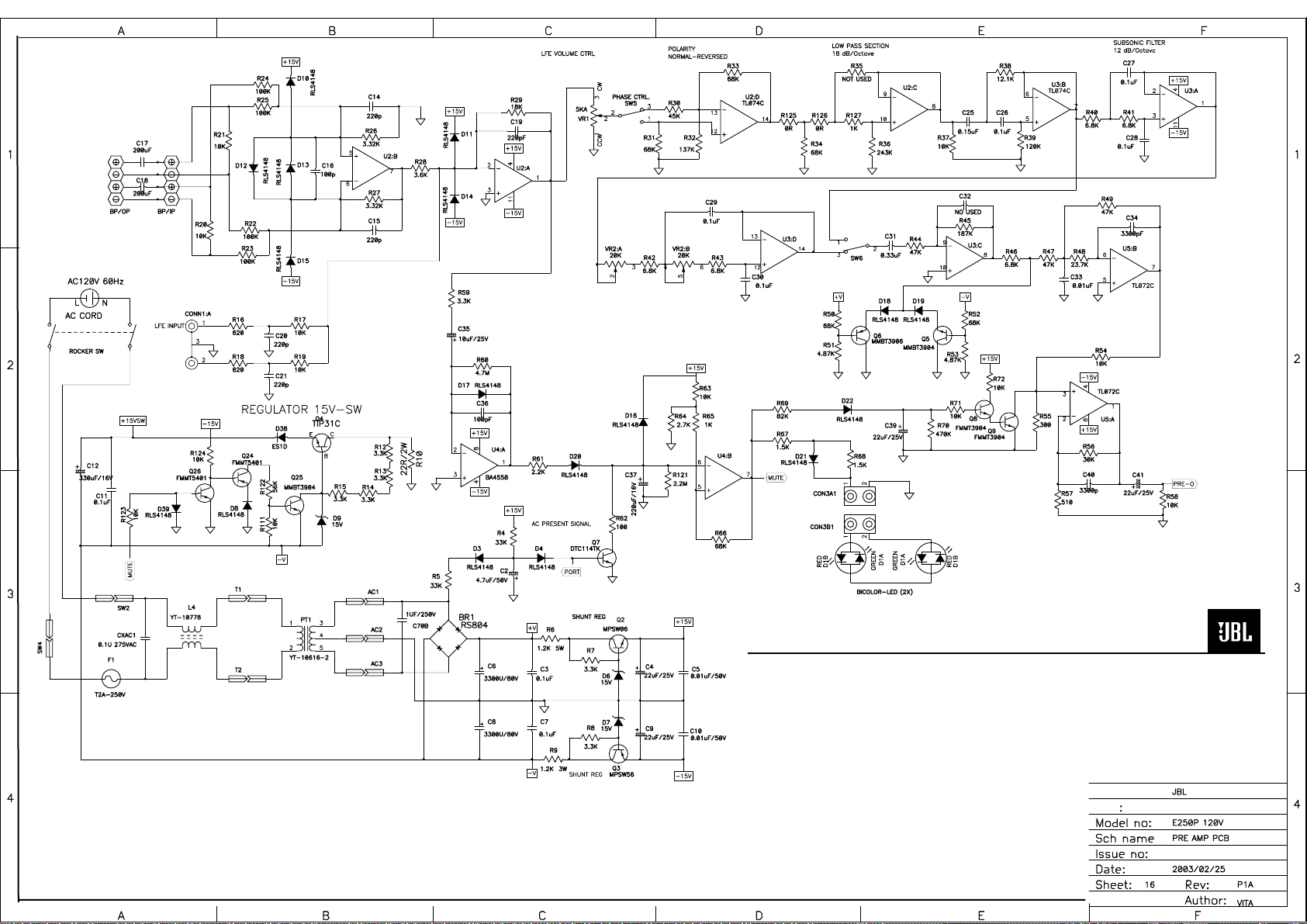
SCHEMATICS
Harman Consumer Group 250 Crossways Park Dr. Woodbury, New York 11797
Email [email protected] Web www.harmanservice.com
Page 22
Page 22
E250P
Harman Consumer Group 250 Crossways Park Dr. Woodbury, New York 11797
Email [email protected] Web www.harmanservice.com
Page 23
S120PII Studio Series
Page 23
Harman Consumer Group 250 Crossways Park Dr. Woodbury, New York 11797
Email [email protected] Web www.harmanservice.com
Page 24

S120PII Studio Series
Page 24
Harman Consumer Group
250 Crossways Park Dr.
Woodbury, New York 11797
Email [email protected]
Web www.harmanservice.com
 Loading...