IXYS IXDP631PI, IXDP630PI Datasheet

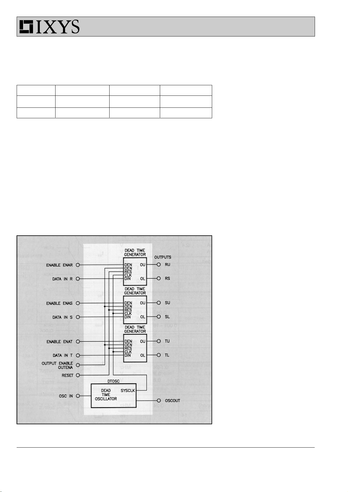
Inverter Interface and Digital Deadtime Generator
for 3-Phase PWM Controls
Type Package Configuration Temp. Range
IXDP630 PI 18-Pin Plastic DIP RC Oscillator -40°C to +85°C
IXDP631 PI 18-Pin Plastic DIP Crystal Oscillator -40°C to +85°C
This 5 V HCMOS integrated circuit is
intended primarily for application in
three-phase, sinusoidally commutated
brushless motor, induction motor, AC
servomotor or UPS PWM modulator
control systems. It injects the required
deadtime to convert a single phase leg
PWM command into the two separate
logic signals required to drive the upper
and lower semiconductor switches in a
PWM inverter. It also provides facilities
for output disable and fast overcurrent
and fault condition shutdown.
In the IXDP630, deadtime programming
is achieved by an internal RC oscillator.
In the IXDP631, programming is
achieved by use of a crystal oscillator.
An alternative for both the IXDP630/
631 is with an external clock signal.
Because of its flexibility, the IXDP630/
631 is easily utilized in a variety of
brushed DC, trapezoidally commutated
brushless DC, hybrid and variable
reluctance step and other more exotic
PWM motor drive power and control
circuit designs.
Block Diagram IXDP 630/IXDP 631
Features
l 5 V HCMOS logic implementation
maintains low power at high speed
l Schmitt trigger inputs and CMOS
logic levels improve noise immunity
l Simultaneously injects equal dead-
time in up to three output phases
l Replaces 10-12 standard SSI/MSI
logic devices
l Allows a wide range of PWM
modulation strategies
l Directly drives high speed
optocouplers
Applications
l 1- and 3- Phase Motion Controls
l 1- and 3- Phase UPS Systems
l General Power Conversion Circuits
l Pulse Timing and Waveform
Generation
l General Purpose Delay and Filter
l General Purpose Three Channel
"One Shot"
IXYS reserves the right to change limits, test conditions and dimensions.
I - 14
© 1998 IXYS All rights reserved

IXDP630
IXDP631
Symbol Definition Maximum Ratings
min. max.
V
CC
V
IN
I
IN
V
0
I
0
T
stg
T
L
Supply Voltage -0.5 7 V
DC Input Voltage -0.5 VCC + 0.5 V
DC Input Current -1 1 mA
DC Output Voltage 0.5 VCC + 0.5 V
DC Output Current -25 25 mA
Storage Temperature -55 150 °C
Lead Soldering (max. 10 s) 300 °C
Recommended Operating Conditions
V
T
l
f
CC
J
0
OSC
Supply Voltage 4.5 5.5 V
Operating Temperature -40 85 °C
Output Current -8 8 mA
Oscillator Frequency 0.001 16/24 MHz
Symbol Definition/Condition Characteristic Values
min. typ. max.
V
V
V
I
C
V
V
I
I
I
t+
t-
HYS
in
in
oh
ol
CC
CCQ
CCQ
Input Hi Threshold 3.6 2.7 V
Input Lo Threshold 1.6 0.8 V
Hysteresis 1.1 V
Input Leakage Current -10 10 µA
Input Capacitance 5 10 pF
Output High Voltage lo = -8 mA 2.4 V
Output Low Voltage lo = 8 mA 0.4 V
Supply Current Outputs Unloaded 5 mA
Quiescent Current Outputs 0.4 1 mA
Unloaded IXDP630
Quiescent Current Outputs 1 10 µA
Unloaded IXDP631
DP630 Oscillator Section
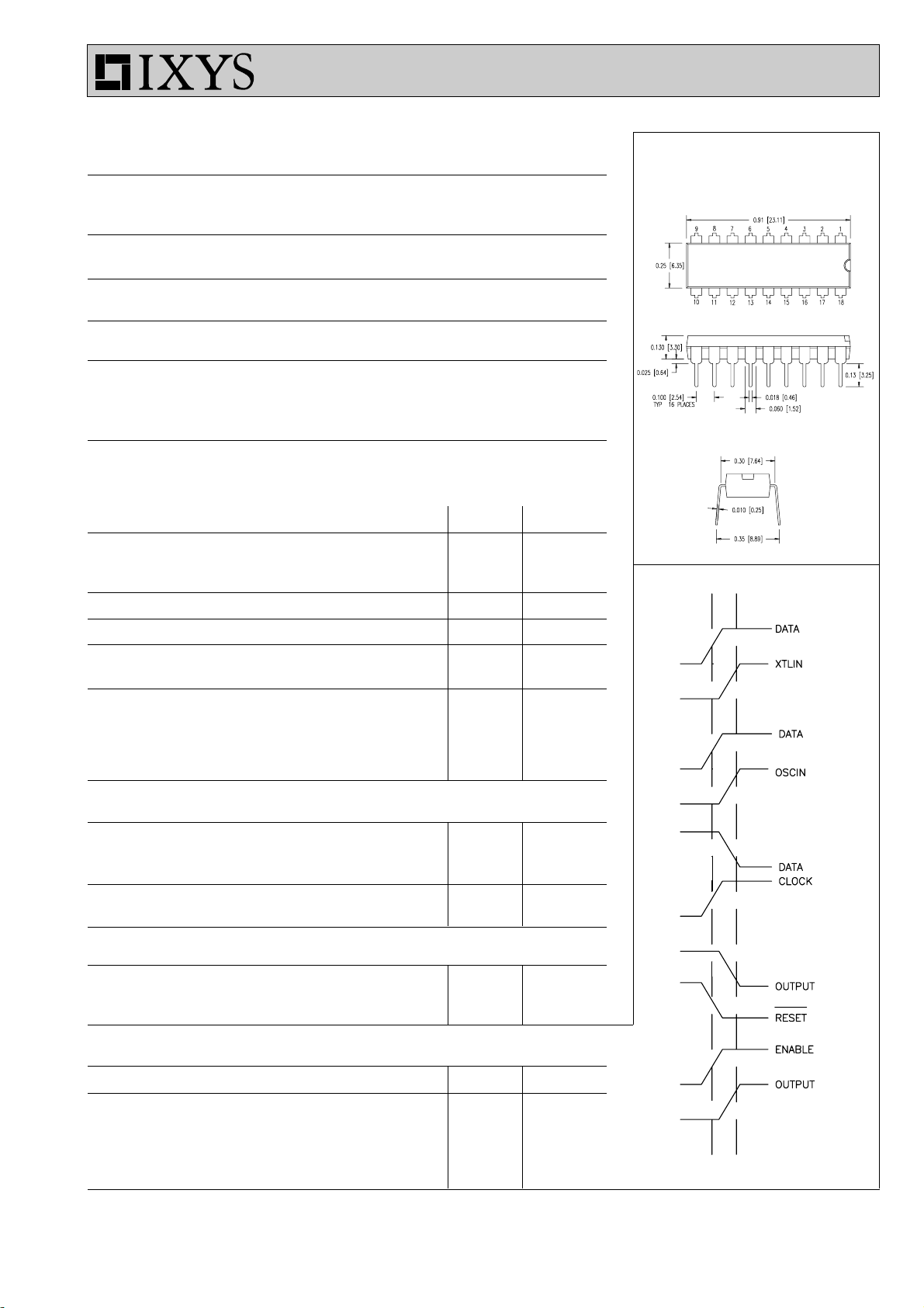
Dimensions in inch (1" = 25.4 mm)
16-Pin Plastic DIP
t
SX
t
SC
C
R
f
OSC
OSC
OSC
Capacitor (RCIN to GND) 0.047 10 nF
Resistor (OSCOUT to RCIN) 1 1000 kΩ
Frequency Range 0.001 - 16 MHz
Initial Tolerance (f
Temperature Coefficient -400 ppm/°C
DP631 Oscillator Section
f
V
V
OSC
INH
INL
Frequency Range 0.1-24 MHz
Oscillator Thresholds (IXTLIN) 3.9 V
External Oscillator
f
t
t
t
t
t
IN
SX
SC
hold
pdro
pdeo
Frequency Range (ODCOUT open) 0-24 MHz
Set Up Time DATA-to-XTLIN 14 nS
Set Up Time DATA-to-OSCIN 22 ns
Hold Time CLOCK-Data 0 ns
Propagation Delay RESET-to-OUTPUT 15 20 ns
Propagation Delay ENABLE-to-OUTPUT 8 16 ns
© 1998 IXYS All rights reserved
≤ 1MHz) 5 %
OSC
0.8 V
t
t
t
hold
pdro
pdeo
I - 15

IXDP630
IXDP631
Pin Description IXDP630
Pin Description IXDP631
Sym. Pin Description
R 1 R, S and T are the three single S 3 phase inputs. Each input is
T 5 expanded into two outputs to
generate non-overlapping drive
signals, RU/RL, SU/SL, and TU/
TL. The delay from the falling
edge of one line to the rising
edge of the other is a function of
the clock.
ENAR 2 High logic input will enable the
ENAS 4 outputs, as set by the proper
ENAT 6 input phase. The ENA (R,S,T)
signals control the drive output
lines. A low logic input will force
both controlled outputs to a low
logic level
OUT 7 High logic level will enable all
ENA outputs to their related phase.
The OUTENA simultaneously
controls all outputs. Low input
logic level will inhibit all outputs
(low).
RESET 8 The RESET signal is active low.
When a logic low RESET is
applied, all outputs will go low.
After releasing the RESET
command within the generated
delay, the outputs will align with
the phase input level after the
programmed delay internal.
Sym. Pin Description
GND 9 CIRCUIT GROUND - 0 Volts
RCIN 10 The first node of the clock
or network. For the IXDP630, the
XTLIN RC input is applied to RCIN. For
OSC 11 This is the output node of the
OUT oscillator. It is connected indi-
TL 12 After the appropriate delay, the
TU 13 external drive outputs (R,S, T) U
SL 14 are in phase with their corres SU 15 ponding inputs; (R,S, T) L are
RL 16 the complementary outputs.
RU 17
V
CC
the IXDP 631, the crystal oscillator is applied to XTLIN. If an
external clock is to be supplied
to the chip it should be connected to this pin.
rectly to the RCIN or XTLIN pins
when using the internal oscillator
as described in the applications
information. It is not recommended for external use.
18 Voltage Supply +5 V ± 10 %
Waveforms
Note: X = Any input, R, S or T.
deadtime
deadtimedeadtime
deadtime deadtime
noise
deadtime
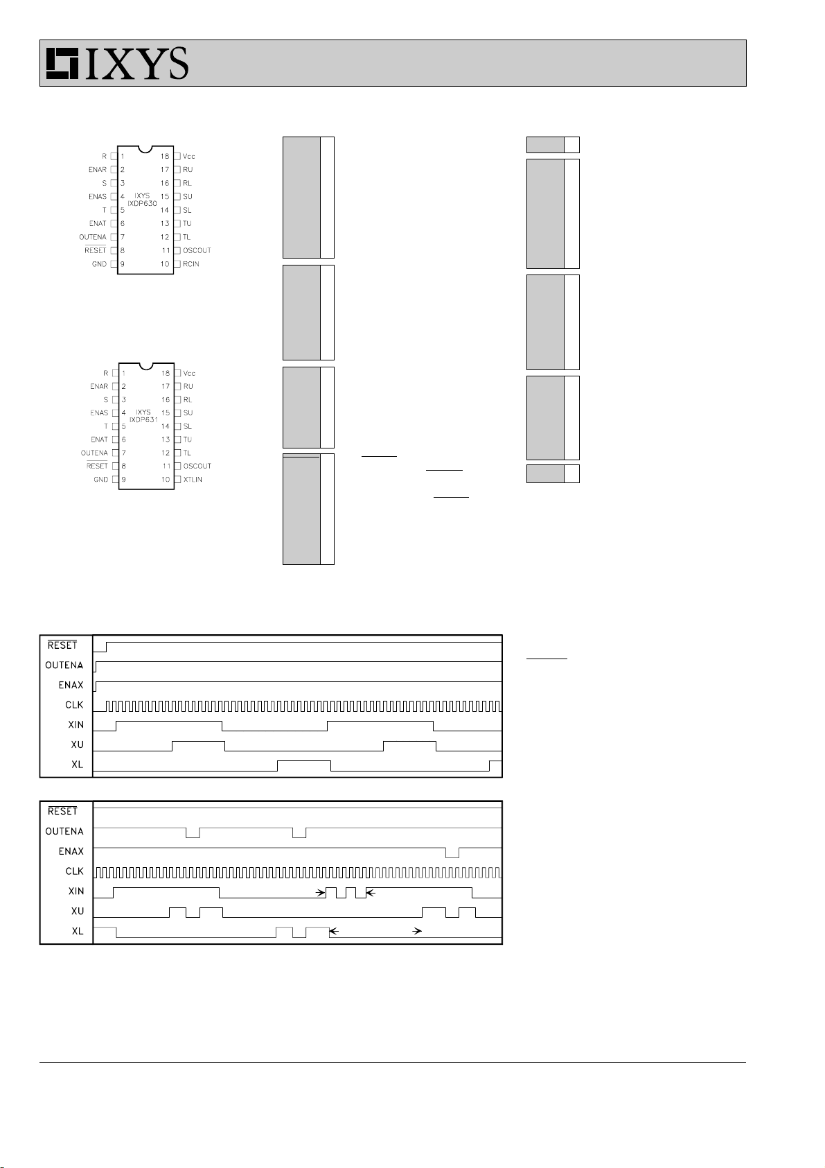
This diagram shows the normal
operation of the IXDP630/631 after the
RESET input is released. The
DEADTIME is the 8 Clock periods
between XU and XL when both XU and
XL are a "0". The length of the
DEADTIME is fixed at 8 times the
period of CLK.
The diagram shows OUTENA and ENAX
asynchronously forcing the XU Output
and the XL Output to the off state.
OUTENA will force all three channels to
the off state. ENAX (where X is one of
the three channels) will only force the
XU and XL Outputs of that channel to
the off state. Note that because ENAX
is asynchronous with respect to the
internal clock and deadtime counters,
when ENAX goes HI whatever state the
deadtime counter was in immediately
propagates to the output. This figure
also shows that noise at the XIN input
will be filtered before the XU Output or
XL Output will become active, which
may extend the deadtime.
I - 16
© 1998 IXYS All rights reserved
 Loading...