IXYS IXDP610PI Datasheet

© 2001 IXYS/DEI All rights reserved
IXDP 610
1
Description
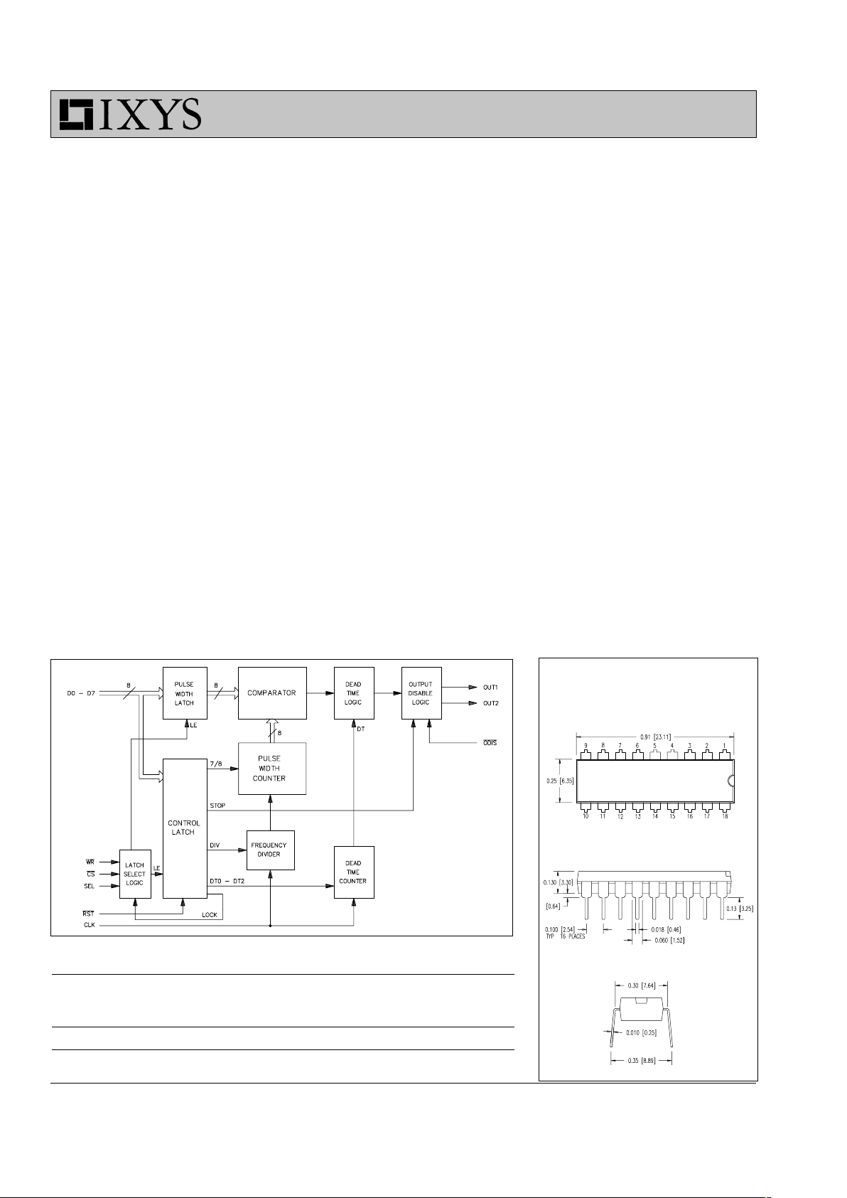
The IXDP610 Digital Pulse Width
Modulator (DPWM) is a programmable
CMOS LSI device which accepts digital
pulse width data from a microprocessor
and generates two complementary,
non-overlapping, pulse width modulated signals for direct digital control of
switching power bridge. The DPWM is
designed to be operated under the
direct control of a microprocessor and
interfaces easily with most standard
microprocessor and microcomputer
buses. The IXDP610 is packaged in an
18-Pin slim DP.
The PWM waveform generated by the
IXDP610 results from comparing the
output of the Pulse Width counter to
the number stored in the Pulse Width
Latch (see below). A programmable
"dead-time" is incorporated into the
PWM waveform. The Dead-Time Logic
disables both outputs on each
transition of the Comparator output for
the required dead-time interval.
The output stage provides complementary PWM output signals capable of
Bus Compatible Digital PWM Controller, IXDP 610
sinking and sourcing 20 mA at TTL
voltage levels. The Output Disable
logic can be activated either by
software or hardware. This facilitates
cycle-by-cycle current-limit, shortcircuit, over-temperature, and
desaturation protection schemes.
The IXDP610 is capable of operating at
PWM frequencies from zero to 390kHz;
the dead-time is programmable from
zero to 14 clock cycles (0 to 11 % of
the PWM cycle), which allows
operation with fast power MOSFETs,
IGBTs, and bipolar power transistors. A
trade-off between PWM frequency and
resolution is provided by selecting the
counter resolution to be 7-bit or 8-bit.
The 20 mA output drive makes the
IXDP610 capable of directly driving
opto isolators and Smart Power
devices. The fast response to pulse
width commands is achieved by
instantaneous change of the outputs to
correspond to the new command. This
eliminates the one-cycle delay usually
associated with other digital PWM
implementations.
Features
● Microcomputer bus compatible
● Two complementary outputs for
direct control of a switching power
bridge
● Dynamically programmable pulse
width ranges from 0 to 100 %
● Two modes of operation: 7-bit or 8-
bit resolution
● Switching frequency range up to
390 kHz
● Programmable Dead-time Counter
prevents switching overlap
● Cycle-by-Cycle disable input to
protect against over-current, overtemperature, etc.
● Outputs may be disabled under
software control
● Special locking bit prevents damage
to the stage in the event of a
software failure
● 18-pin slim DIP package
Dimensions in inch and mm
18-Pin Slim DIP
Symbol Definition Maximum Ratings
V
CC
Supply voltage -0.3 ... 5.5 V
V
IN
Input voltage -0.3 ... VCC + 0.3 V
V
out
Output voltage -0.3 ... VCC + 0.3 V
P
D
Maximum power dissipation 500 mW
T
stg
Storage temperature range -40 ... 125 °C

© 2001 IXYS/DEI All rights reserved 2
IXDP 610
Symbol Definition Maximum Ratings
Operating Range
min. max.
V
CC
Supply voltage 4.5 5.5 V
T
A
Operating free air temperature -40 85 °C
Symbol Definition/Condition Characteristic Values
(Over operating range, unless otherwise specified)
min. typ. max.
V
IH(CMOS)
Input High Voltage ODIS 3.8 VCC +0.3 V
V
IL(CMOS)
Input Low Voltage ODIS -0.3 1.2 V
V
H
Input Hysteresis ODIS 0.3 0.5 V
V
OH
Output High Voltage OUT1 IOH = -20 mA 2.4 V
OUT2
V
OL
Output Low Voltage OUT1 IOL = 20 mA 0.4 V
OUT2
V
IH(TTL)
Input High Voltage All Inputs 2.0 VCC +0.3 V
Except ODIS
V
IL(TTL)
Input Low Voltage All Inputs -0.3 0.8 V
Except ODIS
I
LI
Input Leakage All Inputs -10 -0.1 10 µA
Current 0 < VI < V
CC
I
CC
Power Supply f
CLK
= 5 MHz 3.5 10 mA
Current V
IH
= VCC or 0
Symbol Definition/Condition Characteristic Values
(TA = 25°C, VCC = 5 V ± 10 %, C1 = 50 pF)
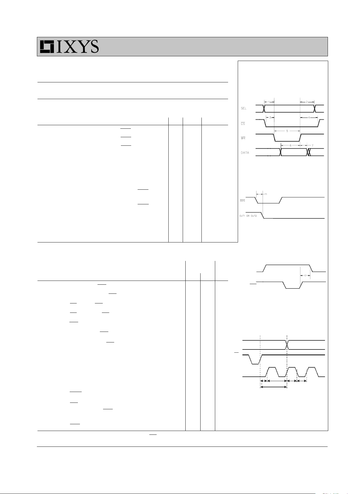
No. see -40...85°C
Fig. 3-6 typ. min. max.
1t
AVWL
SEL Stable to WR Low 5 ns
2t
WHAX
SEL Stable after WR High 10 ns
3t
SLWL
CS Low to WR Low 5 ns
4t
WHSH
CS High after WR High 5 ns
5t
WLWH
WR Pulse Width 8 20 ns
6t
DVWH
Data Valid to WR High 5 ns
7t
WHDX
Data Held after WR High 10 20 ns
8f
CLK
Clock Frequency 50
*
050*MHz
9t
CLCH
Clock Pulse Duration Low 12.5 12.5 ns
t
CHCL
High 12.5 12.5 ns
10 t
CHOV
CLK to Output when 5+½T
CLK
** 5 5+T
CLK
ns
Writing to PW latch
11 t
ODLOL
ODIS Low to Output Low 20 50 ns
12 t
WHOL
WR High to Output Low 30 60 ns
When Writing Stop to the
Control latch
13 t
RLRH
RST Low Time 50 ns
* Output will change 1 rising CLOCK edge +5ns after WR (see Fig. 6)
** T
clk
= 1/f
clk
Numbers in the Fig. 3 to 6 corresponding to the time values on the
bottom left of this page.
Fig. 3 Write operation timing diagram
Fig. 4 Output disable to outputs off
timing
Fig. 5 Stop to outputs off timing
Fig. 6 CLOCK to output when writing
to PW latch
OUT 1 or OUT2
WR
OUT1
OUT2
1
8
10
<5ns 9 9
23
CLK
WR

© 2001 IXYS/DEI All rights reserved
IXDP 610
3
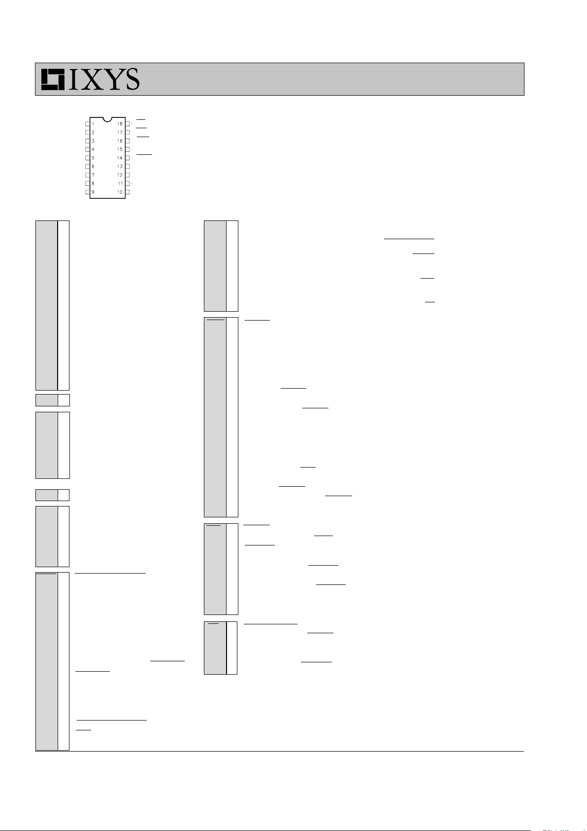
Pin Description IXDP 610PI
Nomenclature of
Digital PWM Controller
Sym. Pin Description
D0 1 DATA BUS - the data bus on
D1 2 the IXDP610 is configured for
D2 3 input only. Data to be written to
D3 4 the IXDP610 is placed on data
D4 5 lines D0 through D7 during a
D5 6 microprocessor write cycle.
D6 7 Data is accepted by the
D7 8 IXDP610 when CHIP SELECT
is low and the WRITE input
goes from a low to a high
state. The SELECT input
determines whether the data
written to the IXDP610 will go
to the Control latch or to the
Pulse Width latch. D0 is the
least significant bit and D7 is
the most significant bit.
GND 9 CIRCUIT GROUND
OUT2 10
COMPLEMENTARY OUTPUTS
OUT1 11 these two outputs provide the
complementary PWM signals.
The base period or cycle time
of these outputs is determined
by the CLOCK and the control
latch.
V
CC
12 POWER SUPPLY (5 V ± 10 %)
CLK 13 CLOCK - the frequency of this
input determines the PWM
base frequency. CLK also
drives the internal state
machines. It has no effect on
any data bus transactions.
ODIS 14 OUTPUT DISABLE - asserting
this Schmitt trigger input forces
the complementary outputs to
be immediately disabled
(OUT1 and OUT2 are forced
low). The complementary
outputs will remain low as long
as long as this input is asserted, and for the duration of the
PWM cycle in which OUTPUT
DISABLE goes from low to
high; i.e., the complementary
outputs are not re-enabled
until the beginning of the next
PWM cycle, and then only if
OUTPUT DISABLE and the
Stop bit in the Control latch are
not asserted.
CS
WR
RST
SEL
ODIS
CLK
V
CC
OUT1
OUT2
D0
D1
D2
D3
D4
D5
D6
D7
GND
SEL 15 SELECT-this input determines
whether data written into the
IXDP610 goes to the internal
Pulse Width (PW) latch or to
the Control latch. A zero on
this input (low voltage) directs
data to the PW latch; a one on
this input (high voltage) directs
data to the Control latch.
RST 16 RESET-this asynchronous,
active low input disables the
outputs, chooses 8-bit count
mode in the PWM counter,
sets the clock to be "divided
by 1", clears Lock bit, and sets
the dead-time counter to 7.
Asserting RESET writes a
01000111 binary to the Control
latch. Asserting RESET is the
only way in which the Lock bit
in the control latch can be
cleared. Writes to the control
latch that occur after the lock
bit has been set to a one, can
only modify the Stop bit. Any
writes to the control latch,
while the RESET input is
asserted, are ignored. RESET
also clears the PW latch.
WR 17 WRITE-a low-to-high transition
on this input, when CHIP
SELECT is low, causes data to
be written to the selected
IXDP610 latch. If SELECT is
low, the data is written to the
pulse width latch. If SELECT is
high, the data is written to the
control latch.
CS 18 CHIP SELECT - this active low
input enables the WRITE input
so that data may be written
into the IXDP610 latch
selected by the SELECT input.
IXDP 610 P I (Example)
IX IXYS
DP 610 Digital PWM Controller
Package Type
P 18-Pin Plastic DIP
Temperature Range
I Industrial
(-40 to 85°C)
IXYS
IXDP610PI
 Loading...