


IT8511E/TE/G
Embedded Controller
Preliminary Specification 0.4.1
ITE TECH. INC.
Specification subject to Change without notice, AS IS and for reference only. For purchasing, please contact sales
representatives.

Copyright © 2006 ITE Tech. Inc.
This is Preliminary document release. All specifications are subject to change without notice.
The material contained in this document supersedes all previous documentation issued for the related products
included herein. Please contact ITE Tech. Inc. for the latest document(s). All sales are subject to ITE’s Standard
Terms and Conditions, a copy of which is included in the back of this document.
ITE, IT8511E/TE/G is a trademark of ITE Tech. Inc.
All other trademarks are claimed by their respective owners.
All specifications are subject to change without notice.
Additional copies of this manual or other ITE literature may be obtained from:
ITE Tech. Inc. Phone: (02) 2912-6889
Marketing Department Fax: (02) 2910-2551, 2910-2552
8F, No. 233-1, Bao Chiao RD., Hsin Tien,
Taipei County 231, Taiwan, R.O.C.
If you have any marketing or sales questions, please contact:
P.Y. Chang, at ITE Taiwan: E-mail: p.y.chang@ite.com.tw, Tel: 886-2-29126889 X6052,
Fax: 886-2-29102551
To find out more about ITE, visit our World Wide Web at:
http://www.ite.com.tw
Or e-mail itesupport@ite.com.tw for more product information/services
Revision History
Section Revision Page No.
7
• In section 7.5.4 Alternate Function Selection, the followings were revised:
1. The “output driving” of GPIOB3-4 was revised to “4“.
2. The “output driving” of GPIOC1-2 was revised to “4“ and GPIOE7 was
revised to “4“.
3. GPIOE0-3 don’t support neither “pull-up” nor “pull-down”.
4. The “default pull” of GPIOI7 was revised to “Up“.
181
www.ite.com.tw IT8511E/TE/G V0.4.1
1 1

Contents
CONTENTS
1. Features ....................................................................................................................................................... 1
2. General Description ....................................................................................................................................... 3
3. System Block Diagram................................................................................................................................... 5
3.1 Block Diagram..................................................................................................................................... 5
3.2 Host/EC Mapped Memory Space ....................................................................................................... 6
3.3 EC Mapped Memory Space................................................................................................................ 9
3.4 Register Abbreviation........................................................................................................................ 10
4. Pin Configuration ......................................................................................................................................... 11
4.1 Top View ........................................................................................................................................... 11
5. Pin Descriptions ........................................................................................................................................... 17
5.1 Pin Descriptions ................................................................................................................................ 17
5.2 Chip Power Planes and Power States.............................................................................................. 23
5.3 Pin Power Planes and States ........................................................................................................... 24
5.4 PWRFAIL# Interrupt to INTC ........................................................................................................... 28
5.5 Reset Sources and Types................................................................................................................. 29
5.5.1 Relative Interrupts to INTC................................................................................................... 29
5.6 Chip Power Mode and Clock Domain............................................................................................... 30
5.7 Pins with Pull, Schmitt-Trigger or Open-Drain Function ................................................................... 34
5.8 Power Consumption Consideration .................................................................................................. 35
6. Host Domain Functions................................................................................................................................ 37
6.1 Low Pin Count Interface.................................................................................................................... 37
6.1.1 Overview............................................................................................................................... 37
6.1.2 Features ............................................................................................................................... 37
6.1.3 Accepted LPC Cycle Type ................................................................................................... 37
6.1.4 Debug Port Function ............................................................................................................ 38
6.1.5 Serialized IRQ (SERIRQ) ..................................................................................................... 39
6.1.6 Relative Interrupts to WUC................................................................................................... 39
6.1.7 LPCPD# and CLKRUN#....................................................................................................... 39
6.1.8 Check Items.......................................................................................................................... 39
6.2 Plug and Play Configuration (PNPCFG)........................................................................................... 40
6.2.1 Logical Device Assignment .................................................................................................. 42
6.2.2 Super I/O Configuration Registers .......................................................................................43
6.2.2.1 Logical Device Number (LDN)................................................................................. 43
6.2.2.2 Chip ID Byte 1 (CHIPID1)........................................................................................ 43
6.2.2.3 Chip ID Byte 2 (CHIPID2)........................................................................................ 43
6.2.2.4 Chip Version (CHIPVER)......................................................................................... 43
6.2.2.5 Super I/O Control Register (SIOCTRL) ................................................................... 43
6.2.2.6 Super I/O IRQ Configuration Register (SIOIRQ)..................................................... 44
6.2.2.7 Super I/O General Purpose Register (SIOGP)........................................................ 44
6.2.2.8 Super I/O Power Mode Register (SIOPWR) ........................................................... 44
6.2.3 Standard Logical Device Configuration Registers................................................................ 45
6.2.3.1 Logical Device Activate Register (LDA)................................................................... 45
6.2.3.2 I/O Port Base Address Bits [15:8] for Descriptor 0 (IOBAD0[15:8]) ........................ 45
6.2.3.3 I/O Port Base Address Bits [7:0] for Descriptor 0 (IOBAD0[7:0]) ............................ 45
6.2.3.4 I/O Port Base Address Bits [15:8] for Descriptor 1 (IOBAD1[15:8]) ........................ 46
6.2.3.5 I/O Port Base Address Bits [7:0] for Descriptor 1 (IOBAD1[7:0]) ............................ 46
6.2.3.6 Interrupt Request Number and Wake-Up on IRQ Enable (IRQNUMX)................... 46
6.2.3.7 Interrupt Request Type Select (IRQTP) .................................................................. 46
6.2.3.8 DMA Channel Select 0 (DMAS0) ............................................................................ 47
6.2.3.9 DMA Channel Select 0 (DMAS1) ............................................................................ 47
6.2.4 System Wake-Up Control (SWUC) Configuration Registers ............................................... 47
6.2.4.1 Logical Device Activate Register (LDA)................................................................... 48
www.ite.com.tw IT8511E/TE/G V0.4.1
i

IT8511E/TE/G
6.2.4.2 I/O Port Base Address Bits [15:8] for Descriptor 0 (IOBAD0[15:8]) ........................ 48
6.2.4.3 I/O Port Base Address Bits [7:0] for Descriptor 0 (IOBAD0[7:0]) ............................ 48
6.2.4.4 I/O Port Base Address Bits [15:8] for Descriptor 1 (IOBAD1[15:8]) ........................ 48
6.2.4.5 I/O Port Base Address Bits [7:0] for Descriptor 1 (IOBAD1[7:0]) ............................ 48
6.2.4.6 Interrupt Request Number and Wake-Up on IRQ Enable (IRQNUMX)................... 48
6.2.4.7 Interrupt Request Type Select (IRQTP) .................................................................. 48
6.2.5 KBC / Mouse Interface Configuration Registers .................................................................. 49
6.2.5.1 Logical Device Activate Register (LDA)................................................................... 49
6.2.5.2 I/O Port Base Address Bits [15:8] for Descriptor 0 (IOBAD0[15:8]) ........................ 49
6.2.5.3 I/O Port Base Address Bits [7:0] for Descriptor 0 (IOBAD0[7:0]) ............................ 49
6.2.5.4 I/O Port Base Address Bits [15:8] for Descriptor 1 (IOBAD1[15:8]) ........................ 49
6.2.5.5 I/O Port Base Address Bits [7:0] for Descriptor 1 (IOBAD1[7:0]) ............................ 50
6.2.5.6 Interrupt Request Number and Wake-Up on IRQ Enable (IRQNUMX)................... 50
6.2.5.7 Interrupt Request Type Select (IRQTP) .................................................................. 50
6.2.6 KBC / Keyboard Interface Configuration Registers.............................................................. 50
6.2.6.1 Logical Device Activate Register (LDA)................................................................... 50
6.2.6.2 I/O Port Base Address Bits [15:8] for Descriptor 0 (IOBAD0[15:8]) ........................ 50
6.2.6.3 I/O Port Base Address Bits [7:0] for Descriptor 0 (IOBAD0[7:0]) ............................ 51
6.2.6.4 I/O Port Base Address Bits [15:8] for Descriptor 1 (IOBAD1[15:8]) ........................ 51
6.2.6.5 I/O Port Base Address Bits [7:0] for Descriptor 1 (IOBAD1[7:0]) ............................ 51
6.2.6.6 Interrupt Request Number and Wake-Up on IRQ Enable (IRQNUMX)................... 51
6.2.6.7 Interrupt Request Type Select (IRQTP) .................................................................. 51
6.2.7 Shared Memory/Flash Interface (SMFI) Configuration Registers ........................................ 51
6.2.7.1 Logical Device Activate Register (LDA)................................................................... 52
6.2.7.2 I/O Port Base Address Bits [15:8] for Descriptor 0 (IOBAD0[15:8]) ........................ 52
6.2.7.3 I/O Port Base Address Bits [7:0] for Descriptor 0 (IOBAD0[7:0]) ............................ 52
6.2.7.4 I/O Port Base Address Bits [15:8] for Descriptor 1 (IOBAD1[15:8]) ........................ 52
6.2.7.5 I/O Port Base Address Bits [7:0] for Descriptor 1 (IOBAD1[7:0]) ............................ 52
6.2.7.6 Interrupt Request Number and Wake-Up on IRQ Enable (IRQNUMX)................... 52
6.2.7.7 Interrupt Request Type Select (IRQTP) .................................................................. 52
6.2.7.8 Shared Memory Configuration Register (SHMC) .................................................... 53
6.2.8 Real Time Clock (RTC) Configuration Registers ................................................................. 53
6.2.8.1 Logical Device Activate Register (LDA)................................................................... 53
6.2.8.2 I/O Port Base Address Bits [15:8] for Descriptor 0 (IOBAD0[15:8]) ........................ 53
6.2.8.3 I/O Port Base Address Bits [7:0] for Descriptor 0 (IOBAD0[7:0]) ............................ 54
6.2.8.4 I/O Port Base Address Bits [15:8] for Descriptor 1 (IOBAD1[15:8]) ........................ 54
6.2.8.5 I/O Port Base Address Bits [7:0] for Descriptor 1 (IOBAD1[7:0]) ............................ 54
6.2.8.6 Interrupt Request Number and Wake-Up on IRQ Enable (IRQNUMX)................... 54
6.2.8.7 Interrupt Request Type Select (IRQTP) .................................................................. 54
6.2.8.8 RAM Lock Register (RLR) ....................................................................................... 54
6.2.8.9 Date of Month Alarm Register Offset (DOMAO) ..................................................... 55
6.2.8.10 Month Alarm Register Offset (MONAO) .................................................................. 55
6.2.8.11 P80L Begin Index (P80LB) ...................................................................................... 55
6.2.8.12 P80L End Index (P80LE)......................................................................................... 55
6.2.8.13 P80L Current Index (P80LC) ................................................................................... 55
6.2.9 Power Management I/F Channel 1 Configuration Registers................................................ 56
6.2.9.1 Logical Device Activate Register (LDA)................................................................... 56
6.2.9.2 I/O Port Base Address Bits [15:8] for Descriptor 0 (IOBAD0[15:8]) ........................ 56
6.2.9.3 I/O Port Base Address Bits [7:0] for Descriptor 0 (IOBAD0[7:0]) ............................ 56
6.2.9.4 I/O Port Base Address Bits [15:8] for Descriptor 1 (IOBAD1[15:8]) ........................ 56
6.2.9.5 I/O Port Base Address Bits [7:0] for Descriptor 1 (IOBAD1[7:0]) ............................ 57
6.2.9.6 Interrupt Request Number and Wake-Up on IRQ Enable (IRQNUMX)................... 57
6.2.9.7 Interrupt Request Type Select (IRQTP) .................................................................. 57
6.2.10 Power Management I/F Channel 2 Configuration Registers................................................ 57
6.2.10.1 Logical Device Activate Register (LDA)................................................................... 57
6.2.10.2 I/O Port Base Address Bits [15:8] for Descriptor 0 (IOBAD0[15:8]) ........................ 58
www.ite.com.tw IT8511E/TE/G V0.4.1
ii

Contents
6.2.10.3 I/O Port Base Address Bits [7:0] for Descriptor 0 (IOBAD0[7:0]) ............................ 58
6.2.10.4 I/O Port Base Address Bits [15:8] for Descriptor 1 (IOBAD1[15:8]) ........................ 58
6.2.10.5 I/O Port Base Address Bits [7:0] for Descriptor 1 (IOBAD1[7:0]) ............................ 58
6.2.10.6 I/O Port Base Address Bits [15:8] for Descriptor 2 (IOBAD2[15:8]) ........................ 58
6.2.10.7 I/O Port Base Address Bits [7:0] for Descriptor 2 (IOBAD2[7:0]) ............................ 58
6.2.10.8 Interrupt Request Number and Wake-Up on IRQ Enable (IRQNUMX)................... 59
6.2.10.9 Interrupt Request Type Select (IRQTP) .................................................................. 59
6.2.11 Programming Guide ............................................................................................................. 60
6.3 Shared Memory Flash Interface Bridge (SMFI) ................................................................................ 62
6.3.1 Overview............................................................................................................................... 62
6.3.2 Features ............................................................................................................................... 62
6.3.3 Function Description............................................................................................................. 62
6.3.3.1 Supported Flash ...................................................................................................... 62
6.3.3.2 Host to M Bus Translation ....................................................................................... 62
6.3.3.3 Memory Mapping ..................................................................................................... 62
6.3.3.4 Host-Indirect Memory Read/Write Transaction ....................................................... 63
6.3.3.5 EC-Indirect Memory Read/Write Transaction.......................................................... 63
6.3.3.6 Locking Between Host and EC Domains................................................................. 64
6.3.3.7 Host Access Protection............................................................................................ 64
6.3.3.8 Response to a Forbidden Access............................................................................ 64
6.3.3.9 Scratch SRAM ......................................................................................................... 64
6.3.3.10 DMA for Scratch SRAM........................................................................................... 66
6.3.3.11 Trusted ROM/RAM .................................................................................................. 66
6.3.3.12 Flash Programming via Host LPC Interface with Scratch SRAM............................ 66
6.3.4 EC Interface Registers ......................................................................................................... 67
6.3.4.1 FBIU Configuration Register (FBCFG) .................................................................... 68
6.3.4.2 Flash Programming Configuration Register (FPCFG)............................................. 68
6.3.4.3 Flash EC Code Banking Select Register (FECBSR)............................................... 69
6.3.4.4 Flash Memory Size Select Register (FMSSR) ........................................................ 70
6.3.4.5 Shared Memory EC Control and Status Register (SMECCS)................................. 71
6.3.4.6 Shared Memory Host Semaphore Register (SMHSR) ............................................ 71
6.3.4.7 Shared Memory EC Override Read Protect Registers 0-1 (SMECORPR0-1) ........ 72
6.3.4.8 Shared Memory EC Override Write Protect Registers 0-1 (SMECOWPR0-1) ....... 72
6.3.4.9 Host Control 2 Register (HCTRL2R) ....................................................................... 72
6.3.4.10 Trusted ROM Register (TROMR) ............................................................................ 73
6.3.4.11 EC-Indirect Memory Address Register 0 (ECINDAR0) ........................................... 73
6.3.4.12 EC-Indirect Memory Address Register 1 (ECINDAR1) ........................................... 73
6.3.4.13 EC-Indirect Memory Address Register 2 (ECINDAR2) ........................................... 73
6.3.4.14 EC-Indirect Memory Address Register 3 (ECINDAR3) ........................................... 73
6.3.4.15 EC-Indirect Memory Data Register (ECINDDR)...................................................... 73
6.3.4.16 Scratch SRAM 0 Address Low Byte Register (SCAR0L) ........................................ 74
6.3.4.17 Scratch SRAM 0 Address Middle Byte Register (SCAR0M)................................... 74
6.3.4.18 Scratch SRAM 0 Address High Byte Register (SCAR0H)....................................... 74
6.3.4.19 Scratch SRAM 1 Address Low Byte Register (SCAR1L) ........................................ 74
6.3.4.20 Scratch SRAM 1 Address Middle Byte Register (SCAR1M)................................... 74
6.3.4.21 Scratch SRAM 1 Address High Byte Register (SCAR1H)....................................... 74
6.3.4.22 Scratch SRAM 2 Address Low Byte Register (SCAR2L) ........................................ 75
6.3.4.23 Scratch SRAM 2 Address Middle Byte Register (SCAR2M)................................... 75
6.3.4.24 Scratch SRAM 2 Address High Byte Register (SCAR2H)....................................... 75
6.3.4.25 Scratch SRAM 3 Address Low Byte Register (SCAR3L) ........................................ 75
6.3.4.26 Scratch SRAM 3 Address Middle Byte Register (SCAR3M)................................... 75
6.3.4.27 Scratch SRAM 3 Address High Byte Register (SCAR3H)....................................... 75
6.3.4.28 Scratch SRAM 4 Address Low Byte Register (SCAR4L) ........................................ 76
6.3.4.29 Scratch SRAM 4 Address Middle Byte Register (SCAR4M)................................... 76
6.3.4.30 Scratch SRAM 4 Address High Byte Register (SCAR4H)....................................... 76
6.3.5 Host Interface Registers....................................................................................................... 76
www.ite.com.tw IT8511E/TE/G V0.4.1
iii

IT8511E/TE/G
6.3.5.1 Shared Memory Indirect Memory Address Register 0 (SMIMAR0) ........................ 76
6.3.5.2 Shared Memory Indirect Memory Address Register 1 (SMIMAR1) ........................ 77
6.3.5.3 Shared Memory Indirect Memory Address Register 2 (SMIMAR2) ........................ 77
6.3.5.4 Shared Memory Indirect Memory Address Register 3 (SMIMAR3) ........................ 77
6.3.5.5 Shared Memory Indirect Memory Data Register (SMIMDR) ................................... 77
6.3.5.6 Shared Memory Host Semaphore Register (SMHSR) ............................................ 77
6.3.5.7 M-Bus Control Register (MBCTRL) ......................................................................... 78
6.4 System Wake-Up Control (SWUC) ................................................................................................... 79
6.4.1 Overview............................................................................................................................... 79
6.4.2 Features ............................................................................................................................... 79
6.4.3 Functional Description.......................................................................................................... 79
6.4.3.1 Wake-Up Status....................................................................................................... 79
6.4.3.2 Wake-Up Events...................................................................................................... 80
6.4.3.3 Wake-Up Output Events.......................................................................................... 81
6.4.3.4 Other SWUC Controlled Options............................................................................. 81
6.4.4 Host Interface Registers....................................................................................................... 83
6.4.4.1 Wake-Up Event Status Register (WKSTR) ............................................................. 83
6.4.4.2 Wake-Up Event Enable Register (WKER)............................................................... 84
6.4.4.3 Wake-Up Signals Monitor Register (WKSMR) ........................................................ 84
6.4.4.4 Wake-Up ACPI Status Register (WKACPIR) .......................................................... 85
6.4.4.5 Wake-Up SMI Enable Register (WKSMIER)........................................................... 85
6.4.4.6 Wake-Up IRQ Enable Register (WKIRQER)........................................................... 86
6.4.5 EC Interface Registers ......................................................................................................... 86
6.4.5.1 SWUC Control Status 1 Register (SWCTL1) ..........................................................86
6.4.5.2 SWUC Control Status 2 Register (SWCTL2) ..........................................................87
6.4.5.3 SWUC Control Status 3 Register (SWCTL3) ..........................................................88
6.4.5.4 SWUC Host Configuration Base Address Low Byte Register (SWCBALR)............ 88
6.4.5.5 SWUC Host Configuration Base Address High Byte Register (SWCBAHR) .......... 88
6.4.5.6 SWUC Interrupt Enable Register (SWCIER)........................................................... 88
6.4.5.7 SWUC Host Event Status Register (SWCHSTR).................................................... 89
6.4.5.8 SWUC Host Event Interrupt Enable Register (SWCHIER) ..................................... 90
6.5 Keyboard Controller (KBC) ............................................................................................................... 91
6.5.1 Overview............................................................................................................................... 91
6.5.2 Features ............................................................................................................................... 91
6.5.3 Functional Description.......................................................................................................... 91
6.5.4 Host Interface Registers....................................................................................................... 92
6.5.4.1 KBC Data Input Register (KBDIR)........................................................................... 93
6.5.4.2 KBC Data Output Register (KBDOR) ...................................................................... 93
6.5.4.3 KBC Command Register (KBCMDR) ...................................................................... 93
6.5.4.4 KBC Status Register (KBSTR) ................................................................................ 93
6.5.5 EC Interface Registers ......................................................................................................... 94
6.5.5.1 KBC Host Interface Control Register (KBHICR)...................................................... 94
6.5.5.2 KBC Interrupt Control Register (KBIRQR)............................................................... 95
6.5.5.3 KBC Host Interface Keyboard/Mouse Status Register (KBHISR) ........................... 96
6.5.5.4 KBC Host Interface Keyboard Data Output Register (KBHIKDOR) ........................ 96
6.5.5.5 KBC Host Interface Mouse Data Output Register (KBHIMDOR) ............................ 96
6.5.5.6 KBC Host Interface Keyboard/Mouse Data Input Register (KBHIDIR) ................... 97
6.6 Power Management Channel (PMC)................................................................................................ 98
6.6.1 Overview............................................................................................................................... 98
6.6.2 Features ............................................................................................................................... 98
6.6.3 Functional Description.......................................................................................................... 98
6.6.3.1 General Description ................................................................................................. 98
6.6.3.2 Compatible Mode..................................................................................................... 99
6.6.3.3 Enhanced PM mode .............................................................................................. 100
6.6.3.4 PMC2EX ................................................................................................................ 101
6.6.4 Host Interface Registers..................................................................................................... 102
www.ite.com.tw IT8511E/TE/G V0.4.1
iv

Contents
6.6.4.1 PMC Data Input Register (PMDIR)........................................................................ 102
6.6.4.2 PMC Data Output Register (PMDOR) ................................................................... 103
6.6.4.3 PMC Command Register (PMCMDR) ................................................................... 103
6.6.4.4 Status Register (PMSTR) ...................................................................................... 103
6.6.5 EC Interface Registers ....................................................................................................... 104
6.6.5.1 PM Status Register (PMSTS)................................................................................ 104
6.6.5.2 PM Data Out Port (PMDO) .................................................................................... 105
6.6.5.3 PM Data Out Port with SCI (PMDOSCI)................................................................ 105
6.6.5.4 PM Data Out Port with SMI (PMDOSMI)............................................................... 105
6.6.5.5 PM Data In Port (PMDI)......................................................................................... 106
6.6.5.6 PM Data In Port with SCI (PMDISCI) .................................................................... 106
6.6.5.7 PM Control (PMCTL) ............................................................................................. 106
6.6.5.8 PM Interrupt Control (PMIC).................................................................................. 107
6.6.5.9 PM Interrupt Enable (PMIE) .................................................................................. 107
6.6.5.10 PM Interrupt Enable (PMIE) .................................................................................. 108
6.6.5.11 16-byte PMC2EX Mailbox 0-15 (MBXEC0-15)...................................................... 108
6.7 Trusted Mobile KBC (TMKBC)........................................................................................................ 109
6.7.1 Overview............................................................................................................................. 109
6.7.2 Features ............................................................................................................................. 109
6.7.3 Functional Description........................................................................................................ 109
6.7.4 Host Interface Registers..................................................................................................... 109
6.7.4.1 TMKBC Vendor ID Register (TVENDID) ............................................................... 109
6.7.4.2 TMKBC Device ID Register (TDEVID) .................................................................. 110
6.7.4.3 TMKBC Version Register (TVER) ......................................................................... 110
6.7.4.4 Generic Capabilities Reporting Register (CAP) .................................................... 110
6.7.4.5 TMKBC Revision ID Register (TREVID)................................................................ 110
6.7.4.6 Configuration Register (CNF) ................................................................................ 111
6.7.4.7 Control Register (CNT).......................................................................................... 111
6.7.4.8 IRQ Capabilities Reporting Register (IRQCAP) .................................................... 112
6.7.4.9 Status Register (STS)............................................................................................ 112
6.7.4.10 Extended Status Register (EXTSTS) .................................................................... 112
6.7.4.11 Interrupt Trigger Enable Register (INTTRIG) ........................................................113
6.7.4.12 TMKBC Data Input Register (TDATIN).................................................................. 113
6.7.4.13 TMKBC Data Output Register (TDATOUT)........................................................... 113
6.7.5 EC Interface Registers ....................................................................................................... 114
6.7.5.1 EC Side Configuration Register (ECCON) ............................................................ 114
6.7.5.2 Status Control Register (STSCON) ....................................................................... 114
6.7.5.3 EC Data Input Register (EDATIN) ......................................................................... 115
6.7.5.4 EC Data Output Register (EDATOUT) .................................................................. 115
6.7.5.5 EC Buffer Status Register (EBUFSTS) ................................................................. 115
6.7.5.6 EC Status Register (ESTS) ...................................................................................115
6.7.5.7 EC Vendor ID Low Register (EVENL) ................................................................... 116
6.7.5.8 EC Vendor ID High Register (EVENH).................................................................. 116
6.7.5.9 EC Device ID Low Register (EDEVL).................................................................... 116
6.7.5.10 EC Device ID High Register (EDEVH) .................................................................. 116
6.7.5.11 EC Version Low Register (EVERL) ....................................................................... 116
6.7.5.12 EC Version High Register (EVERH)...................................................................... 117
6.7.5.13 EC Revision ID Register (EREVID)....................................................................... 117
6.8 Real-Time Clock (RTC)................................................................................................................... 118
6.8.1 Overview............................................................................................................................. 118
6.8.2 Feature ............................................................................................................................... 118
6.8.3 Functional Description........................................................................................................ 118
6.8.3.1 Timekeeping .......................................................................................................... 118
6.8.3.2 Update Cycles ....................................................................................................... 118
6.8.3.3 Interrupts................................................................................................................ 118
6.8.3.4 P80L ...................................................................................................................... 119
www.ite.com.tw IT8511E/TE/G V0.4.1
v

IT8511E/TE/G
6.8.4 Host Interface Registers..................................................................................................... 119
6.8.4.1 RTC Bank 0 Register............................................................................................. 121
6.8.4.1.1 Seconds Register (SECREG) ....................................................... 121
6.8.4.1.2 Seconds Alarm 1 Register (SECA1REG) ...................................... 121
6.8.4.1.3 Minutes Register (MINREG) ......................................................... 122
6.8.4.1.4 Minutes Alarm 1 Register (MINA1REG) ........................................ 122
6.8.4.1.5 Hours Register (HRREG)............................................................... 122
6.8.4.1.6 Hours Alarm 1 Register (HRA1REG)............................................. 122
6.8.4.1.7 Day Of Week Register (DOWREG) ............................................... 122
6.8.4.1.8 Date Of Month Register (DOMREG).............................................. 123
6.8.4.1.9 Month Register (MONREG) ........................................................... 123
6.8.4.1.10 Year Register (YRREG) ................................................................. 123
6.8.4.1.11 RTC Control Register A (CTLREGA)............................................. 123
6.8.4.1.12 RTC Control Register B (CTLREGB)............................................. 124
6.8.4.1.13 RTC Control Register C (CTLREGC) ............................................ 125
6.8.4.1.14 RTC Control Register D (CTLREGD) ............................................ 126
6.8.4.1.15 Date of Month Alarm 1 Register (DOMA1REG)............................. 126
6.8.4.1.16 Month Alarm 1 Register (MONA1REG) ......................................... 126
6.8.4.2 RTC Bank 1 Register............................................................................................. 126
6.8.4.2.1 Seconds Alarm 2 Register (SECA2REG) ...................................... 126
6.8.4.2.2 Minutes Alarm 2 Register (MINA2REG) ........................................ 126
6.8.4.2.3 Hours Alarm 2 Register (HRA2REG)............................................. 127
6.8.4.2.4 Date of Month Alarm 2 Register (DOMA2REG)............................. 127
6.8.4.2.5 Month Alarm 2 Register (MONA2REG) ......................................... 127
6.8.4.3 RTC I/O Register ................................................................................................... 127
6.8.4.3.1 RTC Index Register of Bank 0 (RIRB0) ......................................... 127
6.8.4.3.2 RTC Data Register of Bank 0 (RDRB0)......................................... 127
6.8.4.3.3 RTC Index Register of Bank 1 (RIRB1) ......................................... 128
6.8.4.3.4 RTC Data Register of Bank 1 (RDRB1)......................................... 128
7. EC Domain Functions ................................................................................................................................ 131
7.1 8032 Embedded Controller (EC)..................................................................................................... 131
7.1.1 Overview............................................................................................................................. 131
7.1.2 Features ............................................................................................................................. 131
7.1.3 General Description............................................................................................................ 131
7.1.4 Functional Description....................................................................................................... 131
7.1.5 Memory Organization ......................................................................................................... 132
7.1.6 On-Chip Peripherals........................................................................................................... 133
7.1.7 Timer / Counter................................................................................................................... 135
7.1.8 Idle and Doze/Sleep Mode ................................................................................................. 144
7.1.9 EC Internal Register Description........................................................................................ 144
7.1.9.1 Port 0 Register (P0R) ............................................................................................ 145
7.1.9.2 Stack Pointer Register (SPR) ................................................................................ 145
7.1.9.3 Data Pointer Low Register (DPLR)........................................................................ 145
7.1.9.4 Data Pointer High Register (DPHR) ...................................................................... 145
7.1.9.5 Data Pointer 1 Low Register (DP1LR)................................................................... 145
7.1.9.6 Data Pointer 1 High Register (DP1HR) ................................................................. 145
7.1.9.7 Data Pointer Select Register (DPSR).................................................................... 145
7.1.9.8 Power Control Register (PCON)............................................................................ 146
7.1.9.9 Timer Control Register (TCON)............................................................................. 146
7.1.9.10 Timer Mode Register (TMOD) ............................................................................... 147
7.1.9.11 Timer 0 Low Byte Register (TL0R) ........................................................................ 147
7.1.9.12 Timer 1 Low Byte Register (TL1R) ........................................................................ 147
7.1.9.13 Timer 0 High Byte Register (TH0R)....................................................................... 147
7.1.9.14 Timer 1 Low Byte Register (TH1R) ....................................................................... 148
7.1.9.15 Clock Control Register (CKCON) .......................................................................... 148
7.1.9.16 Port 1 Register (P1R) ............................................................................................148
www.ite.com.tw IT8511E/TE/G V0.4.1
vi

Contents
7.1.9.17 Serial Port Control Register (SCON)..................................................................... 149
7.1.9.18 Serial Port Buffer Register (SBUFR) ..................................................................... 149
7.1.9.19 Port 2 Register (P2R) ............................................................................................149
7.1.9.20 Interrupt Enable Register (IE)................................................................................ 150
7.1.9.21 Port 3 Register (P3R) ............................................................................................150
7.1.9.22 Interrupt Priority Register (IP)................................................................................ 151
7.1.9.23 Status Register (STATUS) ................................................................................... 151
7.1.9.24 Timer 2 Control Register (T2CON)........................................................................ 151
7.1.9.25 Timer Mode Register (T2MOD) ............................................................................. 152
7.1.9.26 Timer 2 Capture Low Byte Register (RCAP2LR) .................................................. 152
7.1.9.27 Timer 2 Capture High Byte Register (RCAP2HR)................................................. 152
7.1.9.28 Timer 2 Low Byte Register (TL2R) ........................................................................ 152
7.1.9.29 Timer 2 High Byte Register (TH2R)....................................................................... 153
7.1.9.30 Program Status Word Register (PSW) .................................................................. 153
7.1.9.31 Watch Dog Timer Control Register (WDTCON).................................................... 153
7.1.9.32 Accumulator Register (ACC) ................................................................................. 154
7.1.9.33 B Register (BR)...................................................................................................... 154
7.1.10 Programming Guide ........................................................................................................... 154
7.1.10.1 Code Snippet of Entering Idle/Doze/Sleep Mode.................................................. 154
7.1.10.2Code snippet of Copying Flash Content to Scratch ROM 4 (MOVC-MOVX by PIO)
.........................................................................................................................................
................................................................................................................................... 155
7.1.10.3 Code snippet of Copying Flash Content to Scratch ROM (DMA) ......................... 156
7.2 Interrupt Controller (INTC) .............................................................................................................. 157
7.2.1 Overview............................................................................................................................. 157
7.2.2 Features ............................................................................................................................. 157
7.2.3 Functional Description........................................................................................................ 157
7.2.3.1 Power Fail Interrupt ...............................................................................................157
7.2.3.2 ROM Match Interrupt ............................................................................................. 157
7.2.3.3 Programmable Interrupts....................................................................................... 157
7.2.4 EC Interface Registers ....................................................................................................... 158
7.2.4.1 Interrupt Status Register 0 (ISR0) ......................................................................... 159
7.2.4.2 Interrupt Status Register 1 (ISR1) ......................................................................... 159
7.2.4.3 Interrupt Status Register 2 (ISR2) ......................................................................... 160
7.2.4.4 Interrupt Status Register 3 (ISR3) ......................................................................... 160
7.2.4.5 Interrupt Enable Register 0 (IER0) ........................................................................160
7.2.4.6 Interrupt Enable Register 1 (IER1) ........................................................................161
7.2.4.7 Interrupt Enable Register 2 (IER2) ........................................................................161
7.2.4.8 Interrupt Enable Register 3 (IER3) ........................................................................161
7.2.4.9 Interrupt Edge/Level-Triggered Mode Register 0 (IELMR0).................................. 161
7.2.4.10 Interrupt Edge/Level-Triggered Mode Register 1 (IELMR1).................................. 162
7.2.4.11 Interrupt Edge/Level-Triggered Mode Register 2 (IELMR2).................................. 162
7.2.4.12 Interrupt Edge/Level-Triggered Mode Register 3 (IELMR3).................................. 162
7.2.4.13 Interrupt Polarity Register 0 (IPOLR0)................................................................... 162
7.2.4.14 Interrupt Polarity Register 1 (IPOLR1)................................................................... 163
7.2.4.15 Interrupt Polarity Register 2 (IPOLR2)................................................................... 163
7.2.4.16 Interrupt Polarity Register 3 (IPOLR3)................................................................... 163
7.2.4.17 Interrupt Vector Register (IVCT)............................................................................ 163
7.2.4.18 8032 INT0# Status (INT0ST)................................................................................. 164
7.2.4.19 Power Fail Register (PFAILR) ............................................................................... 164
7.2.5 INTC Interrupt Assignments ............................................................................................... 165
7.2.6 Programming Guide ........................................................................................................... 167
7.3 Wake-Up Control (WUC) ................................................................................................................ 168
7.3.1 Overview............................................................................................................................. 168
7.3.2 Features ............................................................................................................................. 168
7.3.3 Functional Description........................................................................................................ 168
www.ite.com.tw IT8511E/TE/G V0.4.1
vii

IT8511E/TE/G
7.3.4 EC Interface Registers ....................................................................................................... 168
7.3.4.1 Wake-Up Edge Mode Register (WUEMR1) .......................................................... 168
7.3.4.2 Wake-Up Edge Mode Register (WUEMR2) .......................................................... 169
7.3.4.3 Wake-Up Edge Mode Register (WUEMR3) .......................................................... 169
7.3.4.4 Wake-Up Edge Mode Register (WUEMR4) .......................................................... 169
7.3.4.5 Wake-Up Edge Sense Register (WUESR1).......................................................... 169
7.3.4.6 Wake-Up Edge Sense Register (WUESR2).......................................................... 170
7.3.4.7 Wake-Up Edge Sense Register (WUESR3).......................................................... 170
7.3.4.8 Wake-Up Edge Sense Register (WUESR4).......................................................... 170
7.3.4.9 Wake-Up Enable Register (WUENR1) .................................................................. 171
7.3.4.10 Wake-Up Enable Register (WUENR2).................................................................. 171
7.3.4.11 Wake-Up Enable Register (WUENR3).................................................................. 171
7.3.4.12 Wake-Up Enable Register (WUENR4).................................................................. 171
7.3.5 WUC Input Assignments .................................................................................................... 172
7.3.6 Programming Guide ........................................................................................................... 173
7.4 Keyboard Matrix Scan Controller .................................................................................................... 174
7.4.1 Overview............................................................................................................................. 174
7.4.2 Features ............................................................................................................................. 174
7.4.3 EC Interface Registers ....................................................................................................... 174
7.4.3.1 Keyboard Scan Out Low Byte Data Register (KSOL) ........................................... 174
7.4.3.2 Keyboard Scan Out High Byte Data 1 Register (KSOH1)..................................... 174
7.4.3.3 Keyboard Scan Out Control Register (KSOCTRL)................................................ 174
7.4.3.4 Keyboard Scan Out High Byte Data 2 Register (KSOH2)..................................... 175
7.4.3.5 Keyboard Scan In Data Register (KSIR) ............................................................... 175
7.4.3.6 Keyboard Scan In Control Register (KSICTRLR).................................................. 175
7.5 General Purpose I/O Port (GPIO) ................................................................................................... 176
7.5.1 Overview............................................................................................................................. 176
7.5.2 Features ............................................................................................................................. 176
7.5.3 EC Interface Registers ....................................................................................................... 176
7.5.3.1 General Control Register (GCR) ........................................................................... 176
7.5.3.2 Port Data Registers A-M (GPDRA-GPDRM)......................................................... 177
7.5.3.3 Port Data Mirror Registers A-M (GPDMRA-GPDMRM) ........................................177
7.5.3.4 Port Control n Registers (GPCRn, n = A0-I7)........................................................ 178
7.5.3.5 Output Type Registers A-I (GPOTA-GPOTI)......................................................... 180
7.5.4 Alternate Function Selection .............................................................................................. 181
7.5.5 Programming Guide ........................................................................................................... 186
7.6 EC Clock and Power Management Controller (ECPM) .................................................................. 187
7.6.1 Overview............................................................................................................................. 187
7.6.2 Features ............................................................................................................................. 187
7.6.3 EC Interface Registers ....................................................................................................... 187
7.6.3.1 Clock Frequency Select Register (CFSELR) ........................................................ 187
7.6.3.2 Clock Gating Control 1 Register (CGCTRL1R) ..................................................... 187
7.6.3.3 Clock Gating Control 2 Register (CGCTRL2R) ..................................................... 188
7.6.3.4 Clock Gating Control 3 Register (CGCTRL3R) ..................................................... 189
7.6.3.5 PLL Control (PLLCTRL) ........................................................................................ 189
7.6.3.6 Auto Clock Gating (AUTOCG)............................................................................... 189
7.7 SM Bus Interface (SMB) ................................................................................................................. 191
7.7.1 Overview............................................................................................................................. 191
7.7.2 Features ............................................................................................................................. 191
7.7.3 Functional Description........................................................................................................ 191
7.7.3.1 SMBUS Master Interface....................................................................................... 191
7.7.3.2 SMBUS Porting Guide ........................................................................................... 192
7.7.4 EC Interface Registers ....................................................................................................... 196
7.7.4.1 Host Status Register (HOSTA).............................................................................. 196
7.7.4.2 Host Control Register (HOCTL)............................................................................. 197
7.7.4.3 Host Command Register (HOCMD) ...................................................................... 198
www.ite.com.tw IT8511E/TE/G V0.4.1
viii

Contents
7.7.4.4 Transmit Slave Address Register (TRASLA) ........................................................ 198
7.7.4.5 Data 0 Register (D0REG)...................................................................................... 198
7.7.4.6 Data 1 Register (D1REG)...................................................................................... 198
7.7.4.7 Host Block Data Byte Register (HOBDB) .............................................................. 198
7.7.4.8 Packet Error Check Register (PECERC)............................................................... 199
7.7.4.9 SMBUS Pin Control Register (SMBPCTL) ............................................................ 199
7.7.4.10 Host Control Register 2 (HOCTL2)........................................................................ 199
7.7.4.11 4.7 μs Low Register (4P7USL) .............................................................................. 200
7.7.4.12 4.0 μs Low Register (4P0USL) .............................................................................. 200
7.7.4.13 300 ns Register (300NSREG) ............................................................................... 200
7.7.4.14 250 ns Register (250NSREG) ............................................................................... 200
7.7.4.15 25 ms Register (25MSREG).................................................................................. 200
7.7.4.16 45.3 μs Low Register (45P3USLREG) .................................................................. 201
7.7.4.17 45.3 μs High Register (45P3USHREG)................................................................. 201
7.7.4.18 4.7 μs And 4.0 μs High Register (4p7A4P0H) ....................................................... 201
7.8 PS/2 Interface .................................................................................................................................202
7.8.1 Overview............................................................................................................................. 202
7.8.2 Features ............................................................................................................................. 202
7.8.3 Functional Description........................................................................................................ 202
7.8.3.1 Hardware Mode Selected ...................................................................................... 202
7.8.3.2 Software Mode Selected ....................................................................................... 203
7.8.4 EC Interface Registers ....................................................................................................... 203
7.8.4.1 PS/2 Control Register 1-4 (PSCTL1-4) ................................................................. 203
7.8.4.2 PS/2 Interrupt Control Register 1-4 (PSINT1-4).................................................... 204
7.8.4.3 PS/2 Status Register 1-4 (PSSTS1-4)................................................................... 204
7.8.4.4 PS/2 Data Register 1-4 (PSDAT1-4) ..................................................................... 205
7.9 Digital To Analog Converter (DAC)................................................................................................. 206
7.9.1 Overview............................................................................................................................. 206
7.9.2 Feature ............................................................................................................................... 206
7.9.3 Functional Description........................................................................................................ 206
7.9.4 EC Interface Registers ....................................................................................................... 206
7.9.4.1 DAC Control Register (DACCTRL)........................................................................ 206
7.9.4.2 DAC Data Channel 0~3 Register (DACDAT0~3) .................................................. 207
7.9.4.3 DAC Power Down Register (DACPDREG) ...........................................................207
7.10 Analog to Digital Converter (ADC).................................................................................................. 208
7.10.1 Overview............................................................................................................................. 208
7.10.2 Features ............................................................................................................................. 208
7.10.3 Functional Description........................................................................................................ 208
7.10.3.1 ADC General Description ......................................................................................209
7.10.3.2 Voltage Measurement and Automatic Hardware Calibration ................................ 209
7.10.3.3 ADC Operation ...................................................................................................... 210
7.10.4 EC Interface Registers ....................................................................................................... 211
7.10.4.1 ADC Status Register (ADCSTS) ........................................................................... 211
7.10.4.2 ADC Configuration Register (ADCCFG)................................................................ 212
7.10.4.3 ADC Clock Control Register (ADCCTL) ................................................................ 213
7.10.4.4 Voltage Channel 0 Control Register (VCH0CTL) .................................................. 213
7.10.4.5 Calibration Data Control Register (KDCTL) .......................................................... 214
7.10.4.6 Voltage Channel 1 Control Register (VCH1CTL) .................................................. 215
7.10.4.7 Volt Channel 1 Data Buffer LSB (VCH1DATL)...................................................... 215
7.10.4.8 Volt Channel 1 Data Buffer MSB (VCH1DATM).................................................... 215
7.10.4.9 Voltage Channel 2 Control Register (VCH2CTL) .................................................. 216
7.10.4.10 Volt Channel 2 Data Buffer LSB (VCH2DATL)...................................................... 216
7.10.4.11 Volt Channel 2 Data Buffer MSB (VCH2DATM).................................................... 216
7.10.4.12 Voltage Channel 3 Control Register (VCHN3CTL) ............................................... 216
7.10.4.13 Volt Channel 3 Data Buffer LSB (VCH3DATL)...................................................... 217
7.10.4.14 Volt Channel 3 Data Buffer MSB (VCH3DATM).................................................... 217
www.ite.com.tw IT8511E/TE/G V0.4.1
ix

IT8511E/TE/G
7.10.4.15 Volt High Scale Calibration Data Buffer LSB (VHSCDBL) .................................... 217
7.10.4.16 Volt High Scale Calibration Data Buffer MSB (VHSCDBM) .................................. 217
7.10.4.17 Voltage Channel 0 Data Buffer LSB (VCH0DATL)................................................ 218
7.10.4.18 Voltage Channel 0 Data Buffer MSB (VCH0DATM).............................................. 218
7.10.4.19 Volt High Scale Gain-Error Calibration Data Buffer LSB (VHSGCDBL) ............... 218
7.10.4.20 Volt High Scale Gain-Error Calibration Data Buffer MSB (VHSGCDBM) ............. 218
7.10.5 ADC Programming Guide................................................................................................... 219
7.11 PWM and SmartAuto Fan Control (PWM) ...................................................................................... 222
7.11.1 Overview............................................................................................................................. 222
7.11.2 Features ............................................................................................................................. 222
7.11.3 Functional Description........................................................................................................ 222
7.11.3.1 General Description............................................................................................... 222
7.11.3.2 CR256 Description................................................................................................. 224
7.11.3.3 How to Decide CR256 Duty Time.......................................................................... 224
7.11.3.4 How to Program CR256 PWM............................................................................... 225
7.11.3.5 SmartAuto Fan Control Mode................................................................................ 226
7.11.3.6 Manual Fan Control Mode ..................................................................................... 228
7.11.4 EC Interface Registers ....................................................................................................... 229
7.11.4.1 Channel 0 Clock Prescaler Register (C0CPRS) ................................................... 229
7.11.4.2 Cycle Time Register (CTR) ................................................................................... 230
7.11.4.3 PWM Duty Cycle Register 0 to 7(DCRi) ................................................................ 230
7.11.4.4 PWM Polarity Register (PWMPOL)....................................................................... 230
7.11.4.5 Prescaler Clock Frequency Select Register (PCFSR) .......................................... 231
7.11.4.6 Prescaler Clock Source Select Group Low (PCSSGL) ......................................... 231
7.11.4.7 Prescaler Clock Source Select Group High (PCSSGH)........................................ 232
7.11.4.8 CR256 Prescaler Clock Source Select Group (CR256PCSSG) ........................... 232
7.11.4.9 Prescaler Clock Source Gating Register (PCSGR)............................................... 233
7.11.4.10 Fan 1 Configuration Register (FAN1CNF)............................................................. 233
7.11.4.11 Fan 2 Configuration Register (FAN2CNF)............................................................. 234
7.11.4.12 SmartAuto Fan Minimum-region Speed Range Register (AFMISRR) .................. 235
7.11.4.13 SmartAuto Fan Maximum-region Speed Range Register (AFMASRR)................ 236
7.11.4.14 Min/Off PWM Limit Register (MOPL)..................................................................... 237
7.11.4.15 Fan 1 Minimum PWM Duty Cycle Register (F1MPDCR) ...................................... 237
7.11.4.16 Fan 2 Minimum PWM Duty Cycle Register (F2MPDCR) ...................................... 237
7.11.4.17 Fan 1 Temperature LIMIT Register (F1TLIMITR) ................................................. 238
7.11.4.18 Fan 2 Temperature LIMIT Register (F2TLIMITR) ................................................. 238
7.11.4.19 Fan 1 Absolute Temperature LIMIT Register (F1ATLIMITR)................................ 238
7.11.4.20 Fan 2 Absolute Temperature LIMIT Register (F2ATLIMITR)................................ 239
7.11.4.21 Zone Hysteresis Register (ZHYSR)....................................................................... 239
7.11.4.22 Fan 1 Temperature Record Register (F1TRR)...................................................... 239
7.11.4.23 Fan 2 Temperature Record Register (F2TRR)...................................................... 240
7.11.4.24 Fan 1 Tachometer LSB Reading Register (F1TLRR) ........................................... 240
7.11.4.25 Fan 1 Tachometer MSB Reading Register (F1TMRR) ......................................... 240
7.11.4.26 Fan 2 Tachometer LSB Reading Register (F2TLRR) ........................................... 240
7.11.4.27 Fan 2 Tachometer MSB Reading Register (F2TMRR) ......................................... 240
7.11.4.28 Zone Interrupt Status Control Register (ZINTSCR)............................................... 241
7.11.4.29 Zone Temperature Interrupt Enable Register (ZTIER).......................................... 241
7.11.4.30 Channel 4 Clock Prescaler Register (C4CPRS) ................................................... 242
7.11.4.31 Channel 4 Clock Prescaler MSB Register (C4MCPRS)........................................ 242
7.11.4.32 Channel 6 Clock Prescaler Register (C6CPRS) ................................................... 242
7.11.4.33 Channel 6 Clock Prescaler MSB Register (C6MCPRS)........................................ 243
7.11.4.34 Channel 7 Clock Prescaler Register (C7CPRS) ................................................... 243
7.11.4.35 Channel 7 Clock Prescaler MSB Register (C7MCPRS)........................................ 243
7.11.4.36 Fan 1 Temperature Criterion Register 1-3 (F1TC1-3)........................................... 244
7.11.4.37 Fan 2 Temperature Criterion Register 1-3(F2TC1-3)............................................ 244
7.11.4.38 Fan 1 PWM Duty Cycle Criterion Register 1-3(F1PDC1-3) ..................................244
www.ite.com.tw IT8511E/TE/G V0.4.1
x

Contents
7.11.4.39 Fan 2 PWM Duty Cycle Criterion Register 1-3(F2PDC1-3) ..................................244
7.11.5 PWM Programming Guide .................................................................................................245
7.12 EC Access to Host Controlled Modules (EC2I Bridge)................................................................... 248
7.12.1 Overview............................................................................................................................. 248
7.12.2 Features ............................................................................................................................. 248
7.12.3 Functional Description........................................................................................................ 248
7.12.4 EC Interface Registers ....................................................................................................... 248
7.12.4.1 Indirect Host I/O Address Register (IHIOA)........................................................... 249
7.12.4.2 Indirect Host Data Register (IHD).......................................................................... 249
7.12.4.3 Lock Super I/O Host Access Register (LSIOHA) .................................................. 249
7.12.4.4 Super I/O Access Lock Violation Register (SIOLV)............................................... 250
7.12.4.5 EC to I-Bus Modules Access Enable Register (IBMAE)........................................ 250
7.12.4.6 I-Bus Control Register (IBCTL).............................................................................. 250
7.12.5 EC2I Programming Guide .................................................................................................. 252
7.13 External Timer and External Watchdog (ETWD) ............................................................................ 254
7.13.1 Overview............................................................................................................................. 254
7.13.2 Features ............................................................................................................................. 254
7.13.3 Functional Description........................................................................................................ 254
7.13.3.1 External Timer Operation ...................................................................................... 254
7.13.3.2 External WDT Operation ....................................................................................... 255
7.13.4 EC Interface Registers ....................................................................................................... 255
7.13.4.1 External Timer/WDT Configuration Register (ETWCFG) ...................................... 255
7.13.4.2 External Timer Prescaler Register (ETPSR) ......................................................... 256
7.13.4.3 External Timer Counter High Byte (ETCNTLHR) .................................................. 256
7.13.4.4 External Timer Counter Low Byte (ETCNTLLR) ................................................... 256
7.13.4.5 External Timer/WDT Control Register (ETWCTRL) .............................................. 256
7.13.4.6 External WDT Counter High Byte (EWDCNTLHR) ............................................... 257
7.13.4.7 External WDT Low Counter (EWDCNTLLR)......................................................... 257
7.13.4.8 External WDT Key Register (EWDKEYR)............................................................. 257
7.13.4.9 Reset Scratch Register (RSTSCR) ....................................................................... 257
7.14 General Control (GCTRL) ............................................................................................................... 259
7.14.1 Overview............................................................................................................................. 259
7.14.2 Features ............................................................................................................................. 259
7.14.3 Functional Description........................................................................................................ 259
7.14.4 EC Interface Registers ....................................................................................................... 259
7.14.4.1 Chip ID Byte 1 (ECHIPID1) ................................................................................... 259
7.14.4.2 Chip ID Byte 2 (ECHIPID2) ................................................................................... 260
7.14.4.3 Chip Version (ECHIPVER) .................................................................................... 260
7.14.4.4 Identify Input Register (IDR) .................................................................................. 260
7.14.4.5 Reset Status (RSTS) ............................................................................................. 260
7.14.4.6 Reset Control 1 (RSTC1) ...................................................................................... 261
7.14.4.7 Reset Control 2 (RSTC2) ...................................................................................... 261
7.14.4.8 Reset Control 3 (RSTC3) ...................................................................................... 262
7.14.4.9 Wait Next Clock Rising (WNCKR) ......................................................................... 262
7.14.4.10 Oscillator Control Register (OSCTRL)................................................................... 262
7.14.4.11 Special Control 1 (SPCTRL1)................................................................................ 262
7.14.4.12 Reset Control Host Side (RSTCH) ........................................................................ 263
7.15 Battery-backed SRAM (BRAM)....................................................................................................... 265
7.15.1 Overview............................................................................................................................. 265
7.15.2 Features ............................................................................................................................. 265
7.15.3 Functional Description........................................................................................................ 265
7.15.3.1 P80L ...................................................................................................................... 265
7.15.4 EC Interface Registers ....................................................................................................... 266
7.15.4.1 SRAM Byte n Registers (SBTn, n= 0-255). ........................................................... 266
7.16 Consumer IR (CIR) ......................................................................................................................... 267
7.16.1 Overview............................................................................................................................. 267
www.ite.com.tw IT8511E/TE/G V0.4.1
xi

IT8511E/TE/G
7.16.2 Features ............................................................................................................................. 267
7.16.3 Functional Description........................................................................................................ 267
7.16.3.1 Transmit Operation ................................................................................................ 268
7.16.3.2 Receive Operation ................................................................................................. 268
7.16.3.3 Wakeup(Power On) Controller Programming Sequence ...................................... 268
7.16.4 EC Interface Registers ....................................................................................................... 269
7.16.4.1 CIR Data Register (C0DR) ....................................................................................269
7.16.4.2 CIR Master Control Register (C0MSTCR)............................................................. 270
7.16.4.3 CIR Interrupt Enable Register (C0IER) ................................................................. 270
7.16.4.4 CIR Interrupt Identification Register (C0IIR).......................................................... 271
7.16.4.5 CIR Carrier Frequency Register (C0CFR)............................................................. 271
7.16.4.6 CIR Receiver Control Register (C0RCR) .............................................................. 273
7.16.4.7 CIR Transmitter Control Register (C0TCR)........................................................... 275
7.16.4.8 CIR Slow Clock Control Register (C0SCK) ........................................................... 276
7.16.4.9 CIR Baud Rate Divisor Low Byte Register (C0BDLR) .......................................... 277
7.16.4.10 CIR Baud Rate Divisor High Byte Register (C0BDHR) ......................................... 277
7.16.4.11 CIR Transmitter FIFO Status Register (C0TFSR)................................................. 277
7.16.4.12 CIR Receiver FIFO Status Register (C0RFSR) .................................................... 278
7.16.4.13 CIR Wakeup Code Length Register (C0WCL) ...................................................... 278
7.16.4.14 CIR Wakeup Code Read/Write Register (C0WCR) .............................................. 278
7.16.4.15 CIR Wakeup Power Control/Status Register (C0WPS) ........................................279
7.17 Debugger (DBGR)........................................................................................................................... 280
7.17.1 Overview............................................................................................................................. 280
7.17.2 Features ............................................................................................................................. 280
7.17.3 Functional Description........................................................................................................ 280
7.17.3.1 ROM Address Match Interrupt............................................................................... 280
7.17.3.2 EC Memory Snoop (ECMS) .................................................................................. 280
7.17.4 EC Interface Registers ....................................................................................................... 281
7.17.4.1 Trigger 1 Address Low Byte Register (BKA1L) ..................................................... 281
7.17.4.2 Trigger 1 Address Middle Byte Register (BKA1M) ................................................ 281
7.17.4.3 Trigger 1 Address High Byte Register (BKA1H).................................................... 281
7.17.4.4 Trigger 2 Address Low Byte Register (BKA2L) ..................................................... 281
7.17.4.5 Trigger 2 Address Middle Byte Register (BKA2M) ................................................ 281
7.17.4.6 Trigger 2 Address High Byte Register (BKA2H).................................................... 282
7.17.4.7 Trigger 3 Address Low Byte Register (BKA3L) ..................................................... 282
7.17.4.8 Trigger 3 Address Middle Byte Register (BKA3M) ................................................ 282
7.17.4.9 Trigger 3 Address High Byte Register (BKA3H).................................................... 282
7.18 Parallel Port (PP) ............................................................................................................................ 283
7.18.1 Overview............................................................................................................................. 283
7.18.2 Features ............................................................................................................................. 283
7.18.3 Functional Description........................................................................................................ 283
7.18.3.1 KBS Connection with Parallel Port Connector ...................................................... 283
7.18.3.2 In-System Programming Operation ....................................................................... 283
8. Register List ............................................................................................................................................... 285
9. DC Characteristics ..................................................................................................................................... 295
10. AC Characteristics ..................................................................................................................................... 297
11. Analog Device Characteristics................................................................................................................... 305
12. Package Information.................................................................................................................................. 307
13. Ordering Information.................................................................................................................................. 311
14. Top Marking Information............................................................................................................................ 313
FIGURES
Figure 3-1. Host/Flash and EC/Flash Mapping (General)................................................................................... 6
www.ite.com.tw IT8511E/TE/G V0.4.1
xii

Contents
Figure 3-2. Host/Flash and EC/Flash Mapping (Flash Size = 512k, EC Code = 64k, a specific example) ........ 7
Figure 3-3. EC 8032 Data/Code Memory Map.................................................................................................... 9
Figure 5-1. Power State Transitions.................................................................................................................. 23
Figure 5-2. Clock Tree....................................................................................................................................... 31
Figure 5-3. LED connection............................................................................................................................... 36
Figure 6-1. Host View Register Map via Index-Data Pair ................................................................................. 42
Figure 6-2. Program Flow Chart for PNPCFG .................................................................................................. 61
Figure 6-3. Scratch SRAM in Data Space......................................................................................................... 65
Figure 6-4. Wakeup Event and Gathering Scheme .......................................................................................... 79
Figure 6-5. KBRST# Output Scheme................................................................................................................ 82
Figure 6-6. GA20 Output Scheme..................................................................................................................... 82
Figure 6-7. KBC Host Interface Block Diagram................................................................................................. 91
Figure 6-8. IRQ Control in KBC Module............................................................................................................ 92
Figure 6-9. PMC Host Interface Block Diagram ................................................................................................ 98
Figure 6-10. EC Interrupt Request for PMC...................................................................................................... 99
Figure 6-11. IRQ/SCI#/SMI# Control in PMC Compatible Mode .................................................................... 100
Figure 6-12. IRQ/SCI#/SMI# Control in PMC Enhanced Mode ...................................................................... 101
Figure 6-13. Typical PMC2EX Mailbox Operation .......................................................................................... 102
Figure 6-14. Register Map of RTC .................................................................................................................. 120
Figure 7-1. Interrupt Control System Configuration ........................................................................................ 133
Figure 7-2. Interrupt Response Time .............................................................................................................. 134
Figure 7-3. Timer 0/1 in Mode 0 and Mode 1.................................................................................................. 135
Figure 7-4. Timer 0/1 in Mode 2, Auto-Reload................................................................................................ 136
Figure 7-5. Timer 0 in Mode 3 Two 8-bit Timers ............................................................................................. 136
Figure 7-6. Timer 2: Capture Mode................................................................................................................. 137
Figure 7-7. Timer 2: Auto Reload (DECN = 0) ................................................................................................ 138
Figure 7-8. Timer 2: Auto Reload Mode (DECN = 1) ...................................................................................... 139
Figure 7-9. Timer 2: Clock Out Mode.............................................................................................................. 140
Figure 7-10. Watchdog Timer.......................................................................................................................... 140
Figure 7-11. Serial Port Block Diagram........................................................................................................... 141
Figure 7-12. Data Frame (Mode 1, 2 and 3) ................................................................................................... 142
Figure 7-13. Timer 2 in Baud Rate Generator Mode ...................................................................................... 143
Figure 7-14. INTC Simplified Diagram ............................................................................................................ 166
Figure 7-15. Program Flow Chart for INTC ..................................................................................................... 167
Figure 7-16. WUC Simplified Diagram ............................................................................................................ 173
Figure 7-17. Program Flow Chart for WUC..................................................................................................... 173
Figure 7-18. GPIO Simplified Diagram............................................................................................................ 186
Figure 7-19. ADC Channels Control Diagram................................................................................................. 208
Figure 7-20. ADC Software Calibration Flow .................................................................................................. 220
Figure 7-21. ADC Software Calibration Flow in a Special Case ..................................................................... 221
Figure 7-22. PWM & SmartAuto Fan Block..................................................................................................... 222
Figure 7-23. PWM Clock Tree......................................................................................................................... 223
www.ite.com.tw IT8511E/TE/G V0.4.1
xiii

IT8511E/TE/G
Figure 7-24. CR256 PWM Block Diagram ...................................................................................................... 224
Figure 7-25. CR256 Base Pulse vs. Additional Pulse..................................................................................... 226
Figure 7-26. SmartAuto Mode 0 Fan PWM output vs. Temperature Reading................................................ 227
Figure 7-27. SmartAuto Mode 1 Fan PWM output vs. Temperature Reading................................................ 228
Figure 7-28. Program Flow Chart for PWM Channel Output .......................................................................... 245
Figure 7-29. Program Flow Chart for CR256 PWM Channel Output.............................................................. 246
Figure 7-30. Program Flow Chart for SmartAuto Fan Channel Output........................................................... 247
Figure 7-31. Program Flow Chart for EC2I Read............................................................................................ 252
Figure 7-32. Program Flow Chart for EC2I Write............................................................................................ 253
Figure 7-33. Simplified Diagram...................................................................................................................... 254
Figure 7-34. BRAM Mapping Diagram ............................................................................................................ 265
Figure 7-35. Simplified Diagram...................................................................................................................... 267
Figure 7-36. Parallel Port Female 25-Pin Connector ...................................................................................... 283
Figure 10-1. VSTBY Power-on Reset Timing ................................................................................................. 297
Figure 10-2. Reset Timing.............................................................................................................................. 297
Figure 10-3. Warm Reset Timing .................................................................................................................... 298
Figure 10-4. Wakeup from Doze Mode Timing ............................................................................................... 298
Figure 10-5. Wake Up from Sleep Mode Timing............................................................................................. 298
Figure 10-6. Asynchronous External Wakeup/Interrupt Source Edge Detected Timing................................. 298
Figure 10-7. LPC and SERIRQ Timing ........................................................................................................... 299
Figure 10-8. SWUC Wake Up Timing ............................................................................................................ 299
Figure 10-9. Flash Read Cycle Timing............................................................................................................ 300
Figure 10-10. Flash Write Cycle Timing......................................................................................................... 300
Figure 10-11. PWM Output Timing ................................................................................................................ 301
Figure 10-12. PMC SMI#/SCI# Timing........................................................................................................... 301
Figure 10-13. PMC IBF/SCI# Timing ............................................................................................................. 302
Figure 10-14. PS/2 Receive/Transmit Timing ................................................................................................ 302
Figure 10-15. SMBUS Timing ........................................................................................................................ 303
Figure 10-16. Consumer IR (CIR) Timing ....................................................................................................... 304
TABLES
Table 3-1. Host/Flash Mapping ........................................................................................................................... 7
Table 3-2. EC/Flash Mapping ............................................................................................................................. 8
Table 3-3. Flash Read/Write Protection Controlled by EC Side ......................................................................... 8
Table 3-4. Trusted ROM Range.......................................................................................................................... 8
Table 4-1. Pins Listed in Numeric Order (176-pin LQFP/TQFP) ...................................................................... 13
Table 4-2. Pins Listed in Numeric Order (180-pin TFBGA) .............................................................................. 14
Table 4-3. Pins Listed in Alphabetical Order..................................................................................................... 15
Table 5-1. Pin Descriptions of LPC Bus Interface............................................................................................. 17
Table 5-2. Pin Descriptions of External Flash Interface.................................................................................... 17
Table 5-3. Pin Descriptions of Keyboard Matrix Scan Interface ....................................................................... 18
www.ite.com.tw IT8511E/TE/G V0.4.1
xiv

Contents
Table 5-4. Pin Descriptions of SM Bus Interface .............................................................................................. 18
Table 5-5. Pin Descriptions of PS/2 Interface ................................................................................................... 18
Table 5-6. Pin Descriptions of PWM Interface .................................................................................................. 18
Table 5-7. Pin Descriptions of Wake Up Control Interface ............................................................................... 19
Table 5-8. Pin Descriptions of UART Interface ................................................................................................. 19
Table 5-9. Pin Descriptions of CIR Interface..................................................................................................... 19
Table 5-10. Pin Descriptions of Parallel Port Interface ..................................................................................... 19
Table 5-11. Pin Descriptions of GPIO Interface ................................................................................................ 20
Table 5-12. Pin Descriptions of Hardware Strap............................................................................................... 20
Table 5-13. Pin Descriptions of ADC Input Interface ........................................................................................ 20
Table 5-14. Pin Descriptions of DAC Output Interface ..................................................................................... 21
Table 5-15. Pin Descriptions of Clock ............................................................................................................... 21
Table 5-16. Pin Descriptions of Power/Ground Signals.................................................................................... 21
Table 5-17. Power States.................................................................................................................................. 23
Table 5-18. Quick Table of Power Plane for Pins ............................................................................................. 24
Table 5-19. Pin States of LPC Bus Interface .................................................................................................... 24
Table 5-20. Pin States of External Flash Interface............................................................................................ 25
Table 5-21. Pin States of Keyboard Matrix Scan Interface ............................................................................... 25
Table 5-22. Pin States of SM Bus Interface ...................................................................................................... 25
Table 5-23. Pin States of PS/2 Interface........................................................................................................... 25
Table 5-24. Pin States of PWM Interface.......................................................................................................... 26
Table 5-25. Pin States of Wake Up Control Interface ....................................................................................... 26
Table 5-26. Pin States of UART Interface......................................................................................................... 26
Table 5-27. Pin States of CIR Interface ............................................................................................................ 26
Table 5-28. Pin States of GPIO Interface.......................................................................................................... 26
Table 5-29. Pin States of ADC Input Interface.................................................................................................. 27
Table 5-30. Pin States of DAC Output Interface ............................................................................................... 27
Table 5-31. Pin States of Clock......................................................................................................................... 27
Table 5-32. Reset Sources................................................................................................................................ 29
Table 5-33. Reset Types and Applied Module.................................................................................................. 29
Table 5-34. Clock Types ................................................................................................................................... 30
Table 5-35. Power Saving by EC Clock Operation Mode ................................................................................. 32
Table 5-36. Module Status in Each Power State/Clock Operation ................................................................... 33
Table 5-37. Pins with Pull Function................................................................................................................... 34
Table 5-38. Pins with Schmitt-Trigger Function ................................................................................................ 34
Table 5-39. Signals with Open-Drain Function ................................................................................................. 34
Table 6-1. LPC/FWH Response........................................................................................................................ 38
Table 6-2. Host View Register Map, PNPCFG ................................................................................................. 40
Table 6-3. Host View Register Map, Logical Devices ....................................................................................... 40
Table 6-4. Host View Register Map via Index-Data I/O Pair, Standard Plug and Play Configuration Registers41
Table 6-5. Interrupt Request (IRQ) Number Assignment, Logical Device IRQ via SERIRQ ............................ 41
Table 6-6. Logical Device Number (LDN) Assignments ................................................................................... 42
www.ite.com.tw IT8511E/TE/G V0.4.1
xv

IT8511E/TE/G
Table 6-7. Host View Register Map via Index-Data I/O Pair, SWUC Logical Device ....................................... 47
Table 6-8. Host View Register Map via Index-Data I/O Pair, KBC / Mouse Interface Logical Device.............. 49
Table 6-9. Host View Register Map via Index-Data I/O Pair, KBC / Keyboard Interface Logical Device ......... 50
Table 6-10. Host View Register Map via Index-Data I/O Pair, SMFI Interface Logical Device ........................ 51
Table 6-11. Host View Register Map via Index-Data I/O Pair, RTC Logical Device......................................... 53
Table 6-12. Host View Register Map via Index-Data I/O, PM1 Logical Device ................................................ 56
Table 6-13. Host View Register Map via Index-Data I/O, PM2 Logical Device ................................................ 57
Table 6-14. Mapped Host Memory Address ..................................................................................................... 62
Table 6-15. EC View Register Map, SMFI ........................................................................................................ 67
Table 6-16. Host View Register Map, SMFI...................................................................................................... 76
Table 6-17. Host View Register Map, SWUC ................................................................................................... 83
Table 6-18. EC View Register Map, SWUC...................................................................................................... 86
Table 6-19. Host View Register Map, KBC ....................................................................................................... 92
Table 6-20. EC View Register Map, KBC ......................................................................................................... 94
Table 6-21. Host View Register Map, PMC .................................................................................................... 102
Table 6-22. EC View Register Map, PMC....................................................................................................... 104
Table 6-23. Host View Register Map, TMKBC................................................................................................ 109
Table 6-24. EC View Register Map, TMKBC .................................................................................................. 114
Table 6-25. Host View Register Map, RTC ..................................................................................................... 119
Table 6-26. Host View Register Map via Index-Data I/O Pair, RTC Bank 0 ................................................... 121
Table 6-27. Host View Register Map via Index-Data I/O Pair, RTC Bank 1 ................................................... 121
Table 7-1. 8032 Port Usage ........................................................................................................................... 131
Table 7-2. System Interrupt Table................................................................................................................... 133
Table 7-3. Timer 2 Modes of Operation .......................................................................................................... 139
Table 7-4. Serial Port Signals.......................................................................................................................... 141
Table 7-5. Selecting the Baud Rate Generator(s)........................................................................................... 143
Table 7-6. Internal RAM Map .......................................................................................................................... 144
Table 7-7. EC View Register Map, INTC ........................................................................................................ 158
Table 7-8. INTC Interrupt Assignments........................................................................................................... 165
Table 7-9. EC View Register Map, WUC ........................................................................................................ 168
Table 7-10. WUC Input Assignments.............................................................................................................. 172
Table 7-11. EC View Register Map, KB Scan................................................................................................. 174
Table 7-12. EC View Register Map, GPIO...................................................................................................... 176
Table 7-13. GPIO Alternate Function.............................................................................................................. 181
Table 7-14. EC View Register Map, ECPM .................................................................................................... 187
Table 7-15. EC View Register Map, SMBUS.................................................................................................. 196
Table 7-16. EC View Register Map, PS/2 ....................................................................................................... 203
Table 7-17. EC View Register Map, DAC ....................................................................................................... 206
Table 7-18. EC View Register Map, ADC ....................................................................................................... 211
Table 7-19. Detail Step of ADC Channel Conversion ..................................................................................... 219
Table 7-20. CR256 Waveform ........................................................................................................................ 225
Table 7-21. CR256 Added Additional Pulse Position...................................................................................... 226
www.ite.com.tw IT8511E/TE/G V0.4.1
xvi

Contents
Table 7-22. EC View Register Map, PWM ...................................................................................................... 229
Table 7-23. EC View Register Map, EC2I....................................................................................................... 249
Table 7-24. EC View Register Map, ETWD .................................................................................................... 255
Table 7-25. EC View Register Map, GCTRL................................................................................................... 259
Table 7-26. Modulation Carrier Frequency ..................................................................................................... 272
Table 7-27. Receiver Demodulation Low Frequency (HCFS = 0) .................................................................. 274
Table 7-28. Receiver Demodulation High Frequency (HCFS = 1).................................................................. 275
Table 7-29. I2EC/D2EC Accessable Targets.................................................................................................. 280
Table 7-30. EC View Register Map, DBGR .................................................................................................... 281
Table 9-1. Power Consumption....................................................................................................................... 296
Table 10-1. VSTBY Power-on Reset AC Table .............................................................................................. 297
Table 10-2. Reset AC Table............................................................................................................................ 297
Table 10-3. Warm Reset AC Table ................................................................................................................. 298
Table 10-4. Wakeup from Doze Mode AC Table ............................................................................................ 298
Table 10-5. Wake Up from Sleep Mode AC Table.......................................................................................... 298
Table 10-6. Asynchronous External Wakeup/Interrupt Source Edge Detected AC Table.............................. 299
Table 10-7. LPC and SERIRQ AC Table ........................................................................................................ 299
Table 10-8. SWUC Wake Up AC Table .......................................................................................................... 299
Table 10-9. Flash Read Cycle AC Table......................................................................................................... 300
Table 10-10. Flash Write Cycle AC Table....................................................................................................... 300
Table 10-11. PWM Output AC Table .............................................................................................................. 301
Table 10-12. PMC SMI#/SCI# AC Table......................................................................................................... 301
Table 10-13. PMC IBF/SCI# AC Table ........................................................................................................... 302
Table 10-14. PS/2 Receive/Transmit AC Table .............................................................................................. 302
Table 10-15. SMBUS AC Table ...................................................................................................................... 303
Table 10-16. Consumer IR (CIR) AC Table .................................................................................................... 304
Table 11-1. ADC Characteristics..................................................................................................................... 305
Table 11-2. DAC Characteristics..................................................................................................................... 305
www.ite.com.tw IT8511E/TE/G V0.4.1
xvii

Features
1. Features
8032 Embedded Controller
− Twin Turbo version/3-stage pipeline
− 10MHz for EC domain and 8032 internal timer
− 10MHz for 8032 code-fetch
− Instruction set compatible with standard 8051/2
LPC Bus Interface
− Compatible with the LPC specification v1.1
− Supports I/O read/write
− Supports TMKBC trusted port cycle
− Supports Memory read/write
− Supports FWH read/write
− Serial IRQ
Flash Interface
− Supports external parallel flash with 10 MHz
base clock
− Up to 4M bytes Flash space shared by the host
and EC side (Parallel flash)
− 8-bit data bus
SM Bus Controller
− SM Bus spec. 2.0
− SM Bus host only
− 2 SM Bus channels
System Wake Up Control
− Modem RI# wake up
− Telephone RING# wake up
− IRQ/SMI routing
EC Wake Up Control
− 32 external/internal wake up events
Interrupt Controller
− 32 interrupt events to EC
− Fixed priority
Timer / Watch Dog Timer
− 3 16-bit multi-function timers inside 8032, which
is based on EC clock
− 1 watch dog timer inside 8032, which is based
on EC clock
− 1 external timer in ETWD module, which is
based on 32.768 k clock source
− 1 external WDT in ETWD module, which is
based on 32.768 k clock source
UART
− Full duplex UART
www.ite.com.tw IT8511E/TE/G V0.4.1
ITPM-PN-200644
Specifications subject to Change without Notice By Jimmy Hou, 10/26/2006
ACPI Power Management Channel
− 2 Power Management channels
− Compatible and enhanced mode
−
RTC
− Supports 2 lockable memory areas
− Supports power-switch circuit
− Supports two alarms
Battery-backed SRAM
− EC registers shared with host RTC SRAM
GPIO
− Supports 98-bit GPIO
− Programmable pull up/pull down
− Schmitt trigger for input
KBC Interface
− 8042 style KBC interface
− Legacy IRQ1 and IRQ12
− Fast A20G and KB reset
ADC
− 14 ADC channels (10 external)
− 10-bit ADC resolution (accuracy ±4LSB)
− Digital filter for noise reduction
− Conversion time for 14 channels within 100 ms
DAC
− 4 DAC channels
− 8-bit DAC
PWM with SmartAuto Fan Control
− 8 PWM channels
− SmartAuto Fan control
− Base clock frequency is 32.768 kHz
− 8/16-bit duty cycle resolution
− 8/16-bit common input clock prescaler
− 4 prescalers for 8 PWM output used for devices
with different frequencies
− 2 Tachometers for measuring fan speed
− Complete resolution 256 PWM output
supported. (CR256)”
PS/2 Interface
− 4 PS/2 interface
− Hardware/Software mode selection
KB Matrix Scan
− Hardware keyboard scan
− 18x8 keyboard matrix scan
1

IT8511E/TE/G
In-System Programming
− ISP via parallel port interface on existing KBS
connector
− Fast flash programming with software provided
by ITE
Consumer IR
− Supports 27-58 KHz, 400-500 KHz device
− Supports remote power-on switch
TMKBC
− Supports v0.95
Power Consumption
− Standby with Sleep mode current: 100 μA
Package
− LQFP 176/TQFP 176/TFBGA 180
www.ite.com.tw IT8511E/TE/G V0.4.1
2

General Description
2. General Description
The IT8511 is a highly integrated embedded controller with system functions suitable for mobile system
applications. The IT8511 directly interfaces to the LPC bus and provides ACPI embedded controller function,
keyboard controller (KBC) and matrix scan, external flash interface for system BIOS and EC code, PWM, ADC
and SmartAuto Fan control for hardware monitor, PS/2 interface for external keyboard/mouse devices, RTC,
BRAM, CIR and system wake up functions for system power management. It also supports the external flash
( or EPROM) to be shared by the host and EC side.
www.ite.com.tw IT8511E/TE/G V0.4.1
3

IT8511E/TE/G
This page is intentionally left blank.
www.ite.com.tw IT8511E/TE/G V0.4.1
4
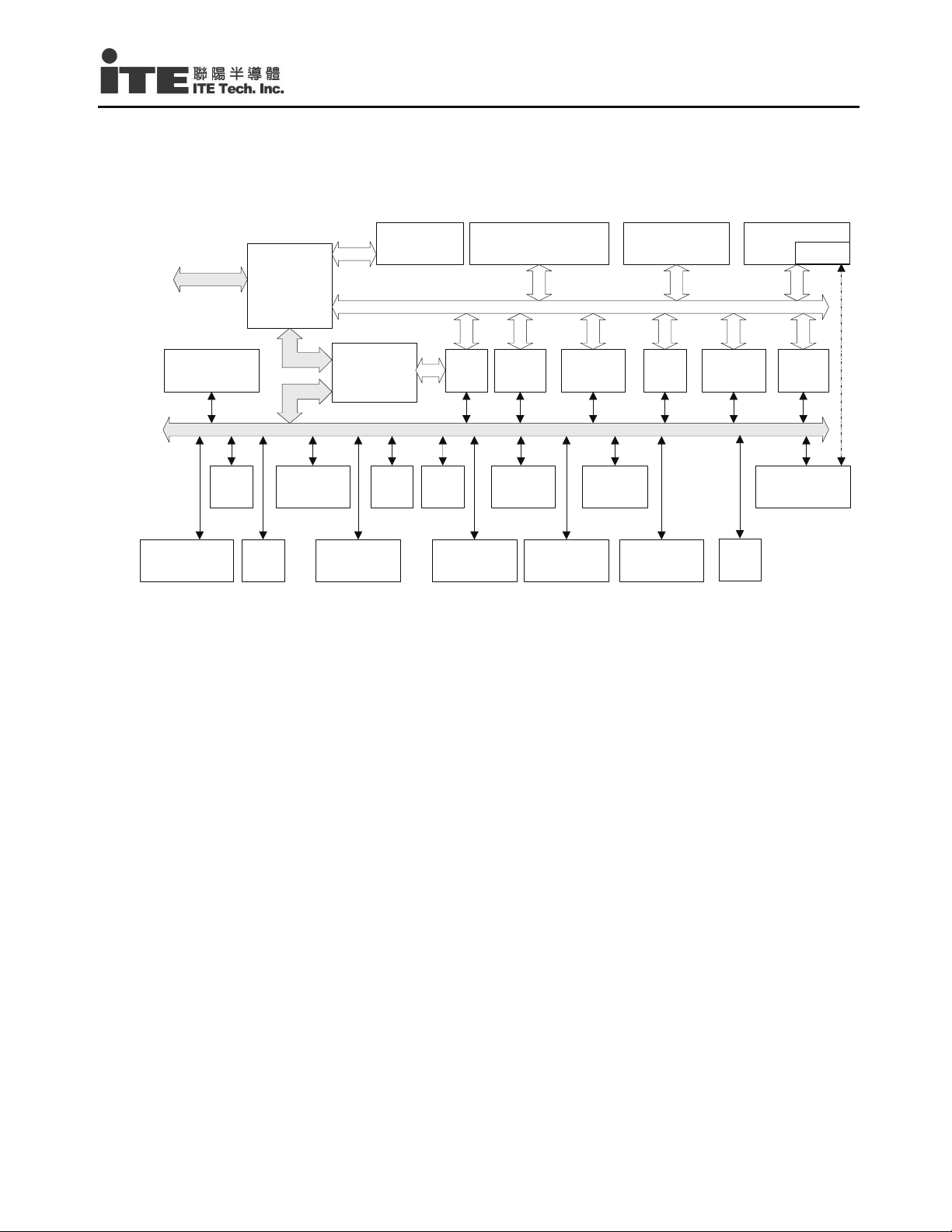
3. System Block Diagram
3.1 Block Diagram
Parallel Flash
M Bus
SMFI
(Flash
Controller)
PP(Parallel
Port)
System Block Diagram
LPC to I Bus / SERIRQ
PNPCFG Regs
Internal Bus(I Bus)
I Bus Arbiter
RTC
SRAM
2K Scratch
SRAM
GCTRL(Gernal
Control)
GPIO
PWM/
SmartAuto
Fan
PS/2
EC
(R8032TT)
DAC
ADC
EC2I
EC Dedicated Bus (EC Bus)
WUC(
SM Bus
ECPM(PMU
Clock Gen)
INTC
WakeUp Ctrl)
TMKBCI2EC
KB Scan
KBC SWUCPMC1/2
ETWD
BRAM(Batterybacked SRAM)
CIR
• Host Domain:
LPC, PNPCFG, RTC logic device, host parts of SMFI/SWUC/KBC/PMC/TMKBC logical devices and host
parts of EC2I.
• EC Domain:
EC 8032, INTC, WUC KB Scan, GPIO, ECPM, SMB, PS/2, DAC, ADC, PWM, HWS, ETWD, EC2I, BRAM,
GCTRL, CIR, EGPC, DBGR, EC parts of SMFI/SWUC/KBC/PMC/TMKBC and EC parts of EC2I.
www.ite.com.tw IT8511E/TE/G V0.4.1
5
IT8511E/TE/G
3.2 Host/EC Mapped Memory Space
Figure 3-1. Host/Flash and EC/Flash Mapping (General)
EC
Code Memory Space
Common Bank
32k
32k
FFFF_FFFFh
FFFF_0000h
FFFE_FFFFh
FFFE_0000h
FFFD_FFFFh
Variable, not necessary
on 32k boundary
1_0000_0000h - Flash_Size
FFFF_FFFFh - Flash_Siz e
Host Memory Space
(byte) (byte)
4G Top Flash Space Top
RANGE 1
RANGE 2
64k
64k
RANGE 3
EC Code:
RANGE 4
Max 160k
Flash_Size
Flash_Size - 1
Flash_Size - 01_0000h
Flash_Size - 01_0001h
Flash_Size - 02_0000h
Flash_Size - 02_0001h
Variable, not necessary
on 32k boundary
00_0000h
Expansion Flash Space
RANGE 1
RANGE 2
RANGE 3
RANGE 4
The range 4 shows space used by EC code and five banks are
all used.
The interface line will be lower if EC code size is smaller than 160K.
(byte)
Bank 3 (32k)
Bank 2 (32k)
Bank 1 (32k)
Bank 0 (32k)
Common Bank (32k)
FFFFh
Bank 0 Bank 1 Bank 3Bank 2
8000h
7FFFh
0000h
000F_FFFFh
000F_0000h
000E_FFFFh
000E_0000h
000D_FFFFh
0000_0000h
Out of Range
RANGE 1
RANGE 2
Out of Range
These five banks are arragned in order and totally 160K mapped.
Each bank is always mapped but it is only valid if it is used by EC code.
If EC code size <= 64K, Bank 0 is valid to be selected.
If EC code size <= 96K, Bank 0-1 are valid to be selected.
If EC code size <= 128K, Bank 0-2 are valid to be selected.
If EC code size <= 160K, Bank 0-3 are valid to be selected.
If EC code size is not mutiple of 32K, the remainder can be
used by host memory.
64k
64k
Bank 0, 1, 2 and 3 occupy the same code memory space.
Only one of these four banks can be selected at once time.
It is selected by ECBB or P1 register.
www.ite.com.tw IT8511E/TE/G V0.4.1
6
System Block Diagram
Figure 3-2. Host/Flash and EC/Flash Mapping (Flash Size = 512k, EC Code = 64k, a specific example)
EC
Code Memory Space
Bank 0
Common Bank
32k
32k
FFFF_FFFFh
FFFF_0000h
FFFE_FFFFh
FFFE_0000h
FFFD_FFFFh
FFF8_FFFFh
FFF8_0000h
FFF7_FFFFh
Host Memory Space
4G Top Flash Space Top
RANGE 1
RANGE 2
RANGE 3
RANGE 4
Out of Range
64k
64k
512k
64k
(byte)(byte)
07_FFFFh
07_0000h
06_FFFFh
06_0000h
05_FFFFh
01_0000hFFF9_0000h
00_FFFFh
00_0000h
Expansion Flash Space
RANGE 1
RANGE 2
RANGE 3
RANGE 4
(byte)
Bank 0 (32k)
Common Bank (32k)
Bank 1-3 are not valid to be selected and are not shown.
FFFFh
8000h
7FFFh
0000h
000F_FFFFh
000F_0000h
000E_FFFFh
000E_0000h
000D_FFFFh
0000_0000h
RANGE 1
RANGE 2
Out of Range
64k
64k
The flash memory space is shared between the host side and EC side, and it is shown in Figure 3-1.
An example of 512k flash size, 64k EC code size is shown in Figure 3-2.
The host memory 4G byte top is always mapped into the top of flash space and the host processor fetches the
first instruction after reset at FFFF_FFF0h in the host memory, which is 16 bytes below the uppermost flash
space.
The bottom of EC code is always mapped into the bottom of flash space and EC R8032TT micro-controller
fetches the first instruction after reset at 00_0000h in the EC code memory, which is 1 byte in the lowermost
flash space.
The interface line of host memory and EC code is variable and not necessary on 32k boundary.
Table 3-1. Host/Flash Mapping
Host Memory Space
on LPC Bus (byte)
(1_0000_0000h–Flash_Size)~
FFFF_FFFFh
000F_0000h ~
000F_FFFFh
000E_0000h ~
000E_FFFFh
Expansion Flash Space (byte)
00_0000h~
(Flash_Size-1)
(Flash_Size-01_0000h)~
(Flash_Size-1)
(Flash_Size-02_0000h)~
(Flash_Size-01_0001h)
Mapped
Size
(byte)
Mapping
Condition
Flash_Size Always
64k Always
64k BIOSEXTS=
1
Note: The host side can map all flash range regardless of EC code space.
Note: All host mappings are controlled by HBREN bit in HCTRL2R register.
Note: Flash Size is defined in FMSSR register.
www.ite.com.tw IT8511E/TE/G V0.4.1
7
IT8511E/TE/G
Table 3-2. EC/Flash Mapping
EC Code
Memory Space (byte)
Flash Address Range
Mapped
(byte)
Size
(byte
)
Mapping
Conditio
n
Bank Selected
Condition
Bank 3: 8000h ~ FFFFh 02_0000h ~ 02_7FFFh 32k Always ECBB=11
Bank 2: 8000h ~ FFFFh 01_8000h ~ 01_FFFFh 32k Always ECBB=10
Bank 1: 8000h ~ FFFFh 01_0000h ~ 01_7FFFh 32k Always ECBB=01
Bank 0: 8000h ~ FFFFh 00_8000h ~ 00_FFFFh 32k Always ECBB=00
Common Bank: 0000h ~ 7FFFh 00_0000h ~ 00_7FFFh 32k Always Always
Note: EC code can use the maximum 160k by banking.
Note: All EC code memory space is mapped to both EC and host side at the same time. The EC size is not
necessary on 32k boundary.
Note:
Note: If BSO=1, ECBB is replaced with P1 register of 8032.
ECBB means ECBB field in FECBSR register.
BSO means BSO bit in FPCFG register.
Table 3-3. Flash Read/Write Protection Controlled by EC Side
Flash Address
Range (byte)
Read Control
Register Bits
Write Control
Register Bits
Note
02_8000h ~ Top ORPLA8 in SMECORPR1 ORPLA8 in SMECOWPR1 Remainder
02_0000h ~ 02_7FFFh ORPLA7 in SMECORPR0 ORPLA7 in SMECOWPR0 32K bytes
01_8000h ~ 01_FFFFh ORPLA6 in SMECORPR0 ORPLA6 in SMECOWPR0 32K bytes
01_0000h ~ 01_7FFFh ORPLA5 in SMECORPR0 ORPLA5 in SMECOWPR0 32K bytes
00_8000h ~ 00_FFFFh ORPLA4 in SMECORPR0 ORPLA4 in SMECOWPR0 32K bytes
00_6000h ~ 00_7FFFh ORPLA3 in SMECORPR0 ORPLA3 in SMECOWPR0 8K bytes
00_4000h ~ 00_5FFFh ORPLA2 in SMECORPR0 ORPLA2 in SMECOWPR0 8K bytes
00_2000h ~ 00_3FFFh ORPLA1 in SMECORPR0 ORPLA1 in SMECOWPR0 8K bytes
00_0000h ~ 00_1FFFh ORPLA0 in SMECORPR0 ORPLA0 in SMECOWPR0 8K bytes
All ranges are write-control by
HOSTWA, too.
Table 3-4. Trusted ROM Range
Flash Address
Trusted ROM Range Enable Note
Range (byte)
02_0000h ~ 02_7FFFh TROMRNG7 in TROMR 32K bytes
01_8000h ~ 01_FFFFh TROMRNG6 in TROMR 32K bytes
01_0000h ~ 01_7FFFh TROMRNG5 in TROMR 32K bytes
00_8000h ~ 00_FFFFh TROMRNG4 in TROMR 32K bytes
00_6000h ~ 00_7FFFh TROMRNG3 in TROMR 8K bytes
00_4000h ~ 00_5FFFh TROMRNG2 in TROMR 8K bytes
00_2000h ~ 00_3FFFh TROMRNG1 in TROMR 8K bytes
00_0000h ~ 00_1FFFh Always 8K bytes
Trusted ROM is where TMKBC firmware locates.
Only Trusted ROM can access Trusted RAM,
which is Scratch RAM with asserted Trust Flag
(TRSF bit in SCAR0H~SCAR4H registers,
respectively). TROMR register can be modified
only by Trusted ROM.
www.ite.com.tw IT8511E/TE/G V0.4.1
8

3.3 EC Mapped Memory Space
Figure 3-3. EC 8032 Data/Code Memory Map
EC Internal EC External EC
Data Memory Space Data Memory Space Code Memory Space
FFFFh
2600h
2500h
2400h
2300h
2200h
2100h
2000h
1F00h
1E00h
1D00h
1C00h
1B00h
1A00h
1900h
1800h
1700h
1600h
1500h
1400h
1300h
1200h
1100h
1000h
0800h
0700h
FFh
7fh
00h
Indirect SFR
Direct & Indirect
corresponging move corresponging read/write corresponging read
instruction: MOV instruction: MOVX instruction: MOVC
0600h
0400h
0000h
System Block Diagram
Reserved
DBGR (byte)
TMKBC
CIR
BRAM
Reserved
GCTRL
ETWD Bank
ECPM 0,1,2 or 3
KB Scan
SM Bus
WUC
DAC
ADC
PWM
PS/2
GPIO
PMC
SWUC
KBC
EC2I Common
INTC Bank
SMFI
0800h-0FFFh=0000h-07FFh
Scratch SRAM No.4 (256B)
Scratch SRAM No.3 (256B)
Scratch SRAM No.2 (512B)
Scratch SRAM No.1 (1024B)
Be a RAM or
RAM/ROM
adjustable
See also Figure 6-3. Scratch SRAM in Data Space on page 65, which also shows Scratch SRAM No 0.
There are five internal Scratch SRAM No 0-4 (No 0 is shared with the same physical SRAM with No 1-4, and is
omitted in Figure 3-3. EC 8032 Data/Code Memory Map), which are always mapped into data space and may
be mapped into code space if their corresponding code space mapping registers are enabled. It means that
Scratch SRAM may be mapped into data and code space at the same time and the firmware on Scratch ROM
can access the same Scratch RAM. It is called Scratch RAM when being located at data space (default after
reset) and called Scratch ROM when being located at code space.
The EC code space is 64k bytes and physically occupies the maximum 160 k bytes at the bottom of the flash
space. Refer to Figure 3-1 on page 6 for the details.
www.ite.com.tw IT8511E/TE/G V0.4.1
9

IT8511E/TE/G
3.4 Register Abbreviation
The register abbreviations and access rules are listed below:
R READ ONLY. If a register is read only, writing to this register has no effect.
W WRITE ONLY. If a register is write only, reading to this register returns all zero.
R/W READ/WRITE. A register with this attribute can be read and written.
RC READ CLEAR. If a register is read clear, reading to this register clears the register to ‘0’.
R/WC READ/WRITE CLEAR. A register bit with this attribute can be read and written. However,
writing 1 clears the corresponding bit and writing 0 has no effect.
BFNAME@REGNAME This abbreviation may be shown in figures to represent one bit in a register or one
field in a register.
The used radix indicator suffixes in this specification are listed below:
Decimal number: "d" suffix or no suffix
Binary number: "b" suffix
Hexadecimal number: "h" suffix
www.ite.com.tw IT8511E/TE/G V0.4.1
10

4. Pin Configuration
4.1 Top View
GPC5
TMRI1/WUI3/GPC6
GPI6
TMRI0/WUI2/GPC4
FCS#
176
175
174
173
46
4847505453
172
49
CK32KOUT/GPC7
PWRSW/GPE4
FA20/GPG4
FA21/GPG5
GA20/GPB5
KBRST#/GPB6
SERIRQ
GPL0
LFRAME#
LAD3
GPL1
GPL2
LAD2
LAD1
LAD0
VCC
VSS
LPCCLK
WRST#
GPL3
GPL4
ECSMI#/GPM0
PWUREQ#/GPM1
LPCPD#/WUI6/GPE6
CLKRUN#/WUI7/GPE7
RI1#/WUI0/GPD0
LPC80HL/GPG6
LPC80LL/GPG7
RI2#/WUI1/GPD1
LPCRST#/WUI4/GPD2
ECSCI#/GPD3
PWM0/GPA0
PWM1/GPA1
VSTBY
VSS
PWM2/GPA2
PWM3/GPA3
PWM4/GPA4
PWM5/GPA5
PWM6/GPA6
GPD4
GINT/GPD5
PWM7/GPA7
WUI5/GP E5
1
2
3
4
5
6
7
8
9
10
11
12
13
14
15
16
17
18
19
20
21
22
23
24
25
26
27
28
29
30
31
32
33
34
35
36
37
38
39
40
41
42
43
44
45
Pin Configuration
IT8511E/TE Top View
SMDAT1/GPC2
GPC3
SMCLK1/GPC1
VSS
GPI5
RING#PWRFAIL#/LPCRST#/GPB7
VSTBY
SMDAT0/GPB4
GPB2
SMCLK0/GPB3
CK32KE
VBAT
VSS
VSTBY
CK32K
GP13
GP14
TXD/GPB1
GP12
RXD/GPB0
FRD#
FWR#
GPI1
FD7
GPI0
FD5
FD6
FD4
FA9/ID1
FA8/ID0
FD2
FD3
FD1
VSS
FD0
VSTBY
FA11/ID3
FA10/ID2
FA7
171
170
169
168
167
166
165
164
163
162
161
160
159
158
157
156
155
154
153
152
151
150
149
148
147
146
145
144
143
142
141
140
139
138
137
136
135
134
133
132
FA6
131
FA5/SHBM
FA12/ID4
130
FA13/ID5
129
FA4/PPEN
128
127
FA3/BADDR1
126
FA2/BADDR0
FA1/TM
125
124
FA0
123
VSTBY
122
VSS
121
FA14/ID6
FA15/ID7
120
119
PS2DAT3/GPF7
118
PS2CLK3/GPF6
117
PS2DAT2/GPF5
116
PS2CLK2/GPF4
115
PS2DAT1/GPF3
114
PS2CLK1/GPF2
113
IT8511
E/TE
Pinout
Top View
52
51
56
585760
55
62
61
59
646366
65
69
686770
72
71
747376
75
787780
82
81
79
8483868887
85
112
111
110
109
108
107
106
105
104
103
102
101
100
99
98
97
96
95
94
93
92
91
90
89
FA16/GPG0
FA17/GPG1
PS2DAT0/GPF1
PS2CLK0/GPF0
GPI7
GPL7
GPL6
GPL5
GPH7
FA18/GPG2
FA19/GPG3
DAC3/GPJ3
DAC2/GPJ2
DAC1/GPJ1
DAC0/GPJ0
GPJ5
GPJ4
AVSS
AVCC
ADC9/GPK5
ADC8/GPK4
CRX/GPM5
CTX/GPM4
ADC7/GPE3
ADC6/GPE2
VSS
GPH0
VSTBY
KSO0/PD0
KSO1/PD1
CLKOUT/GPC0
www.ite.com.tw IT8511E/TE/G V0.4.1
GPH1
GPH2
KSO2/PD2
KSO4/PD4
KSO3/PD3
KSO6/PD6
KSO5/PD5
KSO10/PE
KSO7/PD7
KSO8/ACK#
KSO9/BUSY
TACH0/GPD6
KSO12/SLCT
KSO11/ERR#
TACH1/GPD7
KSO13
KSO14
GPH3
GPH4
KSO15
KSI0/STB#
KSI1/AFD#
KSI2/INIT#
GPH5
KSI3/SLIN#
11
KSI6
KSI7
KSI4
KSI5
GPH6
ADC4/GPE0
ADC1/GPK1
ADC2/GPK2
ADC0/GPK0
ADC3/GPK3
ADC5/GPE1
KSO17/GPM3
KSO16/GPM2

IT8511E/TE/G
IT8511G Top View
SMCLK1/
GPI6 GPC3
FA20/
GPG4
KBRST#/
GPB6
LAD3 SERIRQ
LAD1 LAD2 GPL1 LFRAME#
VCC GPL2 LAD0 GPL3
LPCCLK WRST#
LPCPD#/
GPL4
CLKRUN#/
WUI7/
GPE7
L80LLAT/
GPG7
L80HLAT/
GPC1
TMRI1/
WUI3/
GPC6
FA21/
GPG5
WUI6/
GPE6
GPG6
ECSCI#/
GPD3
SMCLK0/
GPB3
SMDAT1/
GPC2
TMRI0/
WUI2/
GPC4
PWRSW/
GPE4
GPL0
ECSMI#/
GPM0
RI1#/
WUI0/
GPD0
LPCRST#/
WUI4/
GPD2
PWM/
GPA3
PWUREQ#/
VSTBY FRD# FD3
VBAT
GPB2 GPI2
SMDAT0/
GPI5
GPB4
RING#/
PWRFAIL#/
FCS#
LPCRST#/
GPB7
GA20/
GPB5
GPC5
CK32KOUT/
GPC7
RXD/
FWR# FD7
GPB0
CK32K GPI3
CK32KE
GPI4
VSTBY VSS VSTBY VSS VSTBY
TXD/
GPB1
GPI0
IT8511G
Pinout
VSTBY
GPM1
Top View
RI2#/
WUI1/
GPD1
PWM/
GPA4
GINT/
GPD5
VSS
VSTBY VSS
CLKOUT/
GPC0
KSO7 GPH3 KS I5
KSO4 KSO8 KSO13
FA8/
FD4 FD1 FA7
FA9/
KSI2 KSI6
FD2
ID0
FA11/
ID1
ID3
VSS
VSTBYVSS
ADC8/
GPK4
CTX/
GPM4
ADC5/
GPE1
BADDR0
PS2DAT2/
KSO16/
FD0
FA10/
ID2
FA12/
ID4
FA2/
GPF5
GPL7
FA19/
GPG3
DAC1/
GPJ1
ADC7/
GPE3
GPM2
FA6
FA5/
SHBM
BADDR1
FA4/
PP
FA1/TMPS2DAT3/
PS2CLK3/
PS2DAT1/
GPF6
GPI7
PS2DAT0/
GPL6
FA18/
GPG2
GPJ5
ADC9/
GPK5
ADC6/
GPE2
FA13/
ID5
FA3/
FA0
GPF7
GPF3
FA16/
GPG0
GPF1
GPH7 GPL5
DAC2/
GPJ2
GPJ4
CRX/
GPM5
NCNC GPI1 FD6 FD5
FA14/
ID6
FA15/
ID7
PS2CLK2/
GPF4
PS2CLK1/
GPF2
FA17/
GPG1
PS2CLK0/
GPF0
DAC3/
GPJ3
DAC0/
GPJ0
AVSS
PWM0/
PWM1/
GPA0
GPA1
NC
PWM2/
PWM5/
PWM6/
GPA2
PWM7/
GPA5
GPD4 GPH0 KSO2
GPA6
GPA7
WUI5/
GPE5
KSO0
KSO1 KSO5 KSO9 KSO12 GPH4 GPH5
KSO3 GPH2 KSO10 KSO11 KSO15 KSI1
GPH1 KSO6
TACH0/
GPD6
TACH1/
GPD7
KSO14 KSI0
ADC3/
KSI7
GPK3
ADC0/
GPH6
GPK0
KSI3 KSI4
ADC4/
GPE0
ADC2/
GPK2
ADC1/
GPK1
AVCC
KSO17/
GPM3
NC
www.ite.com.tw IT8511E/TE/G V0.4.1
12
Pin Configuration
Table 4-1. Pins Listed in Numeric Order (176-pin LQFP/TQFP)
Pin Signal Pin Signal Pin Signal Pin Signal
CK32KOUT/GPC
1
7
2 PWRSW/GPE4 46 VSS 90 ADC7/GPE3 134 FA11
3 FA20/GPG4 47 CLKOUT/GPC0 91 CTX/GPM4 135 FA10
4 FA21/GPG5 48 GPH0 92 CRX/GPM5 136 VSTBY
5 GA20/GPB5 49 KSO0/PD0 93 ADC8/GPK4 137 VSS
6 KBRST#/GPB6 50 KSO1/PD1 94 ADC9/GPK5 138 FD0
7 SERIRQ 51 KSO2/PD2 95 AVCC 139 FD1
8 GPL0 52 KSO3/PD3 96 AVSS 140 FD2
9 LFRAME# 53 KSO4/PD4 97 GPJ4 141 FD3
10 LAD3 54 GPH1 98 GPJ5 142 FA9
11 GPL1 55 GPH2 99 DAC0/GPJ0 143 FA8
12 GPL2 56 KSO5/PD5 100 DAC1/GPJ1 144 FD4
13 LAD2 57 KSO6/PD6 101 DAC2/GPJ2 145 FD5
14 LAD1 58 KSO7/PD7 102 DAC3/GPJ3 146 FD6
15 LAD0 59 KSO8/ACK# 103 FA19/GPG3 147 FD7
16 VCC 60 KSO9/BUSY 104 FA18/GPG2 148 GPI0
17 VSS 61 KSO10/PE 105 GPH7 149 GPI1
18 LPCCLK 62 TACH0/GPD6 106 GPL5 150 FRD#
19 WRST# 63 TACH1/GPD7 107 GPL6 151 FWR#
20 GPL3 64 KSO11/ERR# 108 GPL7 152 GPI2
21 GPL4 65 KSO12/SLCT 109 GPI7 153 RXD/GPB0
22 ECSMI#/GPM0 66 KSO13 110 PS2CLK0/GPF0 154 TXD/GPB1
23 PWUREQ#/GPM1 67 KSO14 111 PS2DAT0/GPF1 155 GPI3
LPCPD#/WUI6/
24
GPE6
CLKRUN#/WUI7/
25
GPE7
26 RI1#/WUI0/GPD0 70 GPH4 114 PS2CLK1/GPF2 158 CK32K
27 LPC80HL/GPG6 71 KSI0/STB# 115 PS2DAT1/GPF3 159 VSS
28 LPC80LL/GPG7 72 KSI1/AFD# 116 PS2CLK2/GPF4 160 CK32KE
29 RI2#/WUI1/GPD1 73 KSI2/INIT# 117 PS2DAT2/GPF5 161 VBAT
LPCRST#/WUI4/
30
GPD2
31 ECSCI#/GPD3 75 GPH5 119 PS2DAT3/GPF7 163 SMCLK0/GPB3
32 PWM0/GPA0 76 GPH6 120 FA15 164 SMDAT0/GPB4
33 PWM1/GPA1 77 KSI4 121 FA14 165
34 VSTBY 78 KSI5 122 VSS 166 VSTBY
35 VSS 79 KSI6 123 VSTBY 167 VSS
36 PWM2/GPA2 80 KSI7 124 FA0 168 GPI5
37 PWM3/GPA3 81 ADC0/GPK0 125 FA1/TM 169 SMCLK1/GPC1
38 PWM4/GPA4 82 ADC1/GPK1 126 FA2/BADDR0 170 SMDAT1/GPC2
39 PWM5/GPA5 83 ADC2/GPK2 127 FA3/BADDR1 171 GPC3
40 PWM6/GPA6 84 ADC3/GPK3 128 FA4/PPEN 172
41 GPD4 85 KSO16/GPM2 129 FA13 173 FCS#
42 GINT/GPD5 86 KSO17/GPM3 130 FA12 174 GPI6
43 PWM7/GPA7 87 ADC4/GPE0 131 FA5/SHBM 175 GPC5
44 WUI5/GPE5 88 ADC5/GPE1 132 FA6 176
45 VSTBY 89 ADC6/GPE2 133 FA7
68 KSO15 112 FA17/GPG1 156 GPI4
69 GPH3 113 FA16/GPG0 157 VSTBY
74 KSI3/SLIN# 118 PS2CLK3/GPF6 162 GPB2
RING#/
PWRFAIL#/
LPCRST#/GPB7
TMRI0/WUI2/
GPC4
TMRI1/WUI3/
GPC6
www.ite.com.tw IT8511E/TE/G V0.4.1
13

IT8511E/TE/G
Table 4-2. Pins Listed in Numeric Order (180-pin TFBGA)
Pin Signal Pin Signal Pin Signal Pin Signal
A1 NC D4 FCS# H1 LPCCLK L12 ADC6/GPE2
RING#/
A2 SMCLK1/GPC1 D5
PWRFAIL#/
LPCRST#/GPB7
A3 SMCLK0/GPB3 D6 GPI4 H3 ECSMI#/GPM0 L14 AVSS
A4 VBAT D7 CK32KE H4 PWUREQ#/GPM1 M1 PWM0/GPA0
A5 VSTBY D8 GPI0 H5 VSTBY M2 PWM2/GPA2
A6 FRD# D9 FA9/ID1 H10 ADC8/GPK4 M3 PWM6/GPA6
A7 GPI1 D10 FA11/ID3 H11 FA19/GPG3 M4 WUI5/GPE5
A8 FD6 D11 FA12/ID4 H12 FA18/GPG2 M5 KSO1
A9 FD5 D12 FA1/TM H13 GPH7 M6 KSO5
A10 FD3 D13 PS2DAT3/GPF7 H14 GPL5 M7 KSO9
A11 FD0 D14 PS2CLK2/GPF4 J1 GPL4 M8 KSO12
A12 FA6 E1 LAD3 J2
A13 FA13/ID5 E2 SERIRQ J3 RI1#/WUI0/GPD0 M10 GPH5
A14 NC E3 GPL0 J4 RI2#/WUI1/GPD1 M11 KSI7
B1 GPI6 E4 GA20/GPB5 J5 VSS M12 ADC3/GPK3
B2 GPC3 E5 GPC5 J10 CTX/GPM4 M13 ADC4/GPE0
B3 SMDAT1/GPC2 E6 VSTBY J11 DAC1/GPJ1 M14 AVCC
B4 GPB2 E7 VSS J12 GPJ5 N1 PWM1/GPA1
B5 GPI2 E8 VSTBY J13 DAC2/GPJ2 N2 PWM5/GPA5
B6 RXD/GPB0 E9 VSS J14 DAC3/GPJ3 N3 PWM7/GPA7
B7 FWR# E10 VSTBY K1
B8 FD7 E11 FA2/BADDR0 K2 L80HLAT/GPG6 N5 KSO3
B9 FA8/ID0 E12 PS2CLK3/GPF6 K3
B10 FD2 E13 PS2DAT1/GPF3 K4 PWM4/GPA4 N7 KSO10
B11 FA10/ID2 E14 PS2CLK1/GPF2 K5 VSTBY N8 KSO11
B12 FA5/SHBM F1 LAD1 K6 VSS N9 KSO15
B13 FA3/BADDR1 F2 LAD2 K7 KSO7 N10 KSI1
B14 FA14/ID6 F3 GPL1 K8 GPH3 N11 GPH6
C1 FA20/GPG4 F4 LFRAME# K9 KSI5 N12 ADC0/GPK0
TMRI1/WUI3
C2
C3
/GPC6
TMRI0/WUI2
/GPC4
F5 CK32OUT/GPC7 K10 ADC5/GPE1 N13 ADC2/GPK2
F10 VSS K11 ADC7/GPE3 N14 KSO17/GPM3
C4 GPI5 F11 PS2DAT2/GPF5 K12 ADC9/GPK5 P1 NC
C5 SMDAT0/GPB4 F12 GPI7 K13 GPJ4 P2 GPD4
C6 CK32K F13 FA16/GPG0 K14 DAC0/GPJ0 P3 GPH0
C7 GPI3 F14 FA17/GPG1 L1 L80LLAT/GPG7 P4 KSO2
C8 TXD/GPB1 G1 VCC L2 ECSCI#/GPD3 P5 GPH1
C9 FD4 G2 GPL2 L3 PWM3/GPA3 P6 KSO6
C10 FD1 G3 LAD0 L4 GINT/GPD5 P7 TACH0/GPD6
C11 FA7 G4 GPL3 L5 CLKOUT/GPC0 P8 TACH1/GPD7
C12 FA4/PP G5 VSS L6 KSO4 P9 KSO14
C13 FA0 G10 VSTBY L7 KSO8 P10 KSI0
C14 FA15/ID7 G11 GPL7 L8 KSO13 P11 KSI3
D1 KBRST#/GPB6 G12 GPL6 L9 KSI2 P12 KSI4
D2 FA21/GPG5 G13 PS2DAT0/GPF1 L10 KSI6 P13 ADC1/GPK1
D3 PWRSW/GPE4 G14 PS2CLK0/GPF0 L11 KSO16/GPM2 P14 NC
H2 WRST# L13 CRX/GPM5
LPCPD#/WUI6
/GPE6
CLKRUN#/WUI7/
GPE7
LPCRST#/WUI4/
GPD2
M9 GPH4
N4 KSO0
N6 GPH2
www.ite.com.tw IT8511E/TE/G V0.4.1
14

Pin Configuration
Table 4-3. Pins Listed in Alphabetical Order
Signal Pin Signal Pin Signal Pin Signal Pin
ADC0/GPK0 81/N12 FA8/ID0 143/B9 KBRST#/GPB6 6/D1 PS2DAT0/GPF1 111/G13
ADC1/GPK1 82/P13 FA9/ID1 142/D9 KSI0 71/P10 PS2DAT1/GPF3 115/E13
ADC2/GPK2 83/N13 FCS# 173/D4 KSI1 72/N10 PS2DAT2/GPF5 117/F11
ADC3/GPK3 84/M12 FD0 138/A11 KSI2 73/L9 PS2DAT3/GPF7 119/D13
ADC4/GPE0 87/M13 FD1 139/C10 KSI3 74/P11 PWM0/GPA0 32/M1
ADC5/GPE1 88/K10 FD2 140/B10 KSI4 77/P12 PWM1/GPA1 33/N1
ADC6/GPE2 89/L12 FD3 141/A10 KSI5 78/K9 PWM2/GPA2 36/M2
ADC7/GPE3 90/K11 FD4 144/C9 KSI6 79/L10 PWM3/GPA3 37/L3
ADC8/GPK4 93/H10 FD5 145/A9 KSI7 80/M11 PWM4/GPA4 38/K4
ADC9/GPK5 94/K12 FD6 146/A8 KSO0 49/N4 PWM5/GPA5 39/N2
AVCC 95/M14 FD7 147/B8 KSO1 50/M5 PWM6/GPA6 40/M3
AVSS 96/L14 FRD# 150/A6 KSO10 61/N7 PWM7/GPA7 43/N3
CK32K 158/C6 FWR# 151/B7 KSO11 64/N8 PWRSW/GPE4 2/K3
CK32KE 160/D7 GA20/GPB5 5/E4 KSO12 65/M8 PWUREQ#/GPM1 23/H4
CK32KOUT/GP
C7
CLKOUT/GPC0 47/L5 GPB2 162/B4 KSO14 67/P9 RI2#/WUI1/GPD1 29/J4
CLKRUN#/WUI
7/GPE7
CRX/GPM5 92/L13 GPC5 175/E5 KSO16/GPM2 85/L11 RXD/GPB0 153/B6
CTX/GPM4 91/J10 GPD4 41/P2 KSO17/GPM3 86/N14 SERIRQ 7/E2
DAC0/GPJ0 99/K14 GPH0 48/P3 KSO2 51/P4 SMCLK0/GPB3 163/A3
DAC1/GPJ1 100/J11 GPH1 54/P5 KSO3 52/N5 SMCLK1/GPC1 169/A2
DAC2/GPJ2 101/J13 GPH2 55/N6 KSO4 53/L6 SMDAT0/GPB4 164/C5
DAC3/GPJ3 102/J14 GPH3 69/K8 KSO5 56/M6 SMDAT1/GPC2 170/B3
ECSCI#/GPD3 31/L2 GPH4 70/M9 KSO6 57/P6 TACH0/GPD6 62/P7
ECSMI#/GPM0 22/H3 GPH5 75/M10 KSO7 58/K7 TACH1/GPD7 63/P8
FA0 124/C13 GPH6 76/N11 KSO8 59/L7 TMRI0/WUI2/GPC4 172/C3
FA1/TM 125/D12 GPH7 105/H13 KSO9 60/M7 TMRI1/WUI3/GPC6 176/C2
FA10/ID2 135/B11 GPI0 148/D8 L80HLAT/GPG6 27/K2 TXD/GPB1 154/C8
FA11/ID3 134/D10 GPI1 149/A7 L80LLAT/GPG7 28/L1 VBAT 161/A4
FA12/ID4 130/D11 GPI2 152/B5 LAD0 15/G3 VCC 16/G1
FA13/ID5 129/A13 GPI3 155/C7 LAD1 14/F1 17,35,
FA14/ID6 121/B14 GPI4 156/D6 LAD2 13/F2 46,122,
FA15/ID7 120/C14 GPI5 168/C4 LAD3 10/E1 VSS 137,159,
FA16/GPG0 113/F13 GPI6 174/B1 LFRAME# 9/F4 167/E7,
FA17/GPG1 112/F14 GPI7 109/F12 LPCCLK 18/H1 E9,F10,
FA18/GPG2 104/H12 GPJ4 97/K13 LPCPD#/WUI6/GPE6 24/J2
FA19/GPG3 103/H11 GPJ5 98/J12
FA2/BADDR0 126/E11 GPL0 8/E3 NC --/A1 34,45,
FA20/GPG4 3/C1 GPL1 11/F3 NC --/A14 123,136,
FA21/GPG5 4/D2 GPL2 12/G2 NC --/P1 VSTBY 166/
FA3/BADDR1 127/B13 GPL3 20/G4 NC --/P14 E6,E8,
FA4/PP 128/C12 GPL4 21/J1 PS2CLK0/GPF0 110/G14 E10,G10
FA5/SHBM 131/B12 GPL5 106/H14 PS2CLK1/GPF2 114/E14 H5,K5
FA6 132/A12 GPL6 107/G12 PS2CLK2/GPF4 116/D14 WRST# 19/H2
FA7 133/C11 GPL7 108/G11 PS2CLK3/GPF6 118/E12 WUI5/GPE5 44/M4
1/F5 GINT/GPD5 42/L4 KSO13 66/L8 RI1#/WUI0/GPD0 26/J3
25/K1 GPC3 171/B2 KSO15 68/N9
LPCRST#/WUI4/GP
D2
30/K3 VSTBY (PLL) 157/A5
RING#/PWRFAIL#/L
PCRST#/GPB7
165/D5
G5,J5,
K6
www.ite.com.tw IT8511E/TE/G V0.4.1
15

IT8511E/TE/G
This page is intentionally left blank.
www.ite.com.tw IT8511E/TE/G V0.4.1
16
5. Pin Descriptions
5.1 Pin Descriptions
Table 5-1. Pin Descriptions of LPC Bus Interface
Pin(s) No. Signal Attribute Description
LPC Bus Interface (3.3V CMOS I/F, 5V tolerant)
165 or 30 LPCRST#
18 LPCCLK
10, 13-15 LAD[3:0]
9 LFRAME#
24 LPCPD#
25 CLKRUN#
7 SERIRQ
22 ECSMI#
31 ECSCI#
5 GA20
6 KBRST#
19 WRST#
23 PWUREQ#
27 LPC80HL
28 LPC80LL
Table 5-2. Pin Descriptions of External Flash Interface
Pin(s) No. Signal Attribute Description
Flash Interface (3.3V CMOS I/F, 5V tolerant)
120-121,
129-130,
134-135,
142-143,
133-131,
128-124
3-4,
103-104,
112-113
147-144,
141-138
FA[15:0]
FA[21:16]
FD[7:0]
IK LPC Hardware Reset
LPC hardware reset will reset LPC interface and host side modules. The
source is determined by EC side register bit LPCRSTEN.
This pin can be omitted if external LPC reset is not required.
PI LPC Clock
33 MHz clock for LPC domain functions.
PIO LPC Address Data
PI LPC LFRAME# Signal
IO2 LPC LPCPD# Signal
IO6 LPC CLKRUN# Signal
PIO SERIRQ Signal
O8 EC SMI# Signal
This is SMI# signal driven by SWUC module.
O8 EC SCI# Signal
This is SCI# signal driven by PMC module.
IO2 Gate A20 Signal
This is GA20 signal driven by SWUC module.
IO2 KB Reset Signal
This is KBRST# signal driven by SWUC module.
IK Warm Reset
For EC domain function reset after power up.
WRST# is not 5V tolerant.
O2 System Power On Request
This is PWUREQ# signal driven by SWUC module.
O4 LPC I/O Port 80, High-nibble LAD Latch
An active high signal to latch Port 80 high-nibble for the debug
purpose.
O4 LPC I/O Port 80, Low-nibble LAD Latch
An active high signal to latch Port 80 low-nibble for the debug
purpose.
O4 Flash Address [15:0]
These are dedicated external Flash address pins. In addition to being the
Flash address output, FA[5:2] serve as hardware strap pins described
below.
FA[5] : SHBM, shared BIOS mode enable.
FA[4] : PPEN, enable in-system programming via parallel port interface
FA[3] : BADDR[1], used in PNPCFG base address.
FA[2] : BADDR[0], used in PNPCFG base address.
IOK4 Flash Address [21:16]/Alternate GPIO
These pins can be used as GPIO pins depending on the external Flash
size.
IOK4 Flash Data [7:0]
Flash data bus.
Please do not place pull-up resistor on these pins.
Pin Descriptions
www.ite.com.tw IT8511E/TE/G V0.4.1
17

IT8511E/TE
/
G
Pin(s) No. Signal Attribute Description
150 FRD#
151 FWR#
173 FCS#
O4 Flash Read
Flash read control.
Please do not place pull-up resistor on this pin.
O4 Flash Write
Flash write control.
Please do not place pull-up resistor on this pin.
O4 Flash Chip Select
FCS# is the external Flash chip select.
Please do not place pull-up resistor on this pin.
Table 5-3. Pin Descriptions of Keyboard Matrix Scan Interface
Pin(s) No. Signal Attribute Description
KB Matrix Interface (3.3V CMOS I/F, 5V tolerant)
86-85
68-64,
61-56,
53-49
80-77,
74-71
KSO[17:0]
KSI[7:0]
O8 Keyboard Scan Output
Keyboard matrix scan output.
IK Keyboard Scan Input
Keyboard matrix scan input for switch based keyboard.
Table 5-4. Pin Descriptions of SM Bus Interface
Pin(s) No. Signal Attribute Description
SM Bus Interface (3.3V CMOS I/F, 5V tolerant)
169, 163 SMCLK[1:0]
170, 164 SMDAT[1:0]
IOK2 SM Bus CLK
2 SM bus interface provided.
SMCLK0-1 correspond to channel A and B, respectively.
IOK2 SM Bus Data
2 SM bus interface provided.
SMDAT0-1 correspond to channel A and B, respectively.
Table 5-5. Pin Descriptions of PS/2 Interface
Pin(s) No. Signal Attribute Description
PS/2 Interface (3.3V CMOS I/F, 5V tolerant)
118, 116,
114, 110,
119, 117
115, 111
PS2CLK[3:0]
PS2DAT[3:0]
IOK8 PS/2 CLK
4 sets of PS/2 interface, alternate function of GPIO.
PS2CLK0-3 correspond to channel 1-4, respectively.
IOK8 PS/2 Data
4 sets of PS/2 interface, alternate function of GPIO.
PS2DAT0-3 correspond to channel 1-4, respectively.
Table 5-6. Pin Descriptions of PWM Interface
Signal Pin(s) No. Attribute Description
PWM Interface (3.3V CMOS I/F, 5V tolerant)
43, 40-36,
33-32
63-62 TACH[1:0]
176,172 TMRI[1:0]
PWM[7:0]
IOK8 Pulse Width Modulation Output
Two of the eight PWM outputs can be selected as SmartAuto fan control if
enabled. Others are general-purpose PWM signals.
PWM0-7 correspond to channel 0-7, respectively.
IOK2 Tachometer Input
TACH[1:0] are tachometer inputs from external fans. They are used for
measuring the external fan speed.
IOK2 Counter Input
TMRI[1:0] are timer/counter input signals connected to timer2 and timer1 of
8032. Notice that the frequency must be slower than 8032 clock to be
sampled.
www.ite.com.tw IT8511E/TE/G V0.4.1
18

Pin Descriptions
Table 5-7. Pin Descriptions of Wake Up Control Interface
Pin(s) No. Signal Attribute Description
Wake Up Control Interface (3.3V CMOS I/F, 5V tolerant)
25-24,
44, 30,
176, 172,
29, 26
2 PWRSW
29,26 RI[2:1]#
165 RING#
WUI[7:0]
IOK2-8 EC Wake Up Input
Supplied by VSTBY, used for EC wake up.
IOK2 Power Switch Input
Supplied by VSTBY, used to indicate the status of power switch.
IOK4 Ring Indicator Input
Supplied by VSTBY, used for system wake up.
IOK2 Telephone Line Ring Input
Supplied by VSTBY, used for system wake up.
Table 5-8. Pin Descriptions of UART Interface
Pin(s) No. Signal Attribute Description
UART Interface (3.3V CMOS I/F, 5V tolerant)
154 TXD
153 RXD
IOK2 UART TX Output
UART TX Output from 8032
IOK2 UART RX Input
UART RX Input from 8032
Table 5-9. Pin Descriptions of CIR Interface
Pin(s) No. Signal Attribute Description
CIR Interface (3.3V CMOS I/F, 5V tolerant)
91
92
CTX
CRX
IOK2 CIR TX Output
Transmission data for CIR interface
IOK2 CIR RX Input
Receive data for CIR interface
Table 5-10. Pin Descriptions of Parallel Port Interface
Pin(s) No. Signal Attribute Description
ADC Interface (3.3V CMOS I/F)
65 SLCT
61 PE
60 BUSY
59 ACK#
74 SLIN#
73 INIT#
64 ERR#
72 AFD#
71 STB#
58-56,
53-49
PD[7:0]
O8 Printer Select
O8 Printer Paper End
O8 Printer Busy
O8 Printer Acknowledge
IK Printer Select Input
IK Printer Initialize
O8 Printer Error
IK Printer Auto Line Feed
IK Printer Strobe
O8 Parallel Port Data[7:0]
*: The interface can be connected to parallel port of computer through ITE-specified cable. The programmer can
directly read/write flash through this interface.
www.ite.com.tw IT8511E/TE/G V0.4.1
19

IT8511E/TE
/
G
Table 5-11. Pin Descriptions of GPIO Interface
Pin(s) No. Signal Attribute Description
GPIO Interface (3.3V CMOS I/F, 5V tolerant)
Refer to
Pins List
Table
42 GINT
GPA[7:0],
GPB[7:0],
GPC[7:0],
GPD[7:0],
GPE[7:0],
GPF[7:0],
GPG[7:0],
GPH[7:0],
GPI[7:0]
GPJ[5:0]
GPK[5:0]
GPL[7:0]
GPM[5:0]
IOK
Refer to
Table 7-13
on page
181 for
output
driving
capability
IK General Purpose Interrupt
GPIO Signals
The 98 GPIO pins are divided into 13 groups. Each of them contains 8
GPIO pins. Some GPIO pins have alternative function.
General Purpose Interrupt directly input to INT28 of INTC.
Table 5-12. Pin Descriptions of Hardware Strap
Pin(s) No. Signal Attribute Description
Hardware Strap (3.3V CMOS I/F, 5V tolerant)
131 SHBM
128 PPEN
127,126 BADDR[1:0]
125 TM
120-121,
129-130,
134-135,
142-143
ID[7:0]
I Share Host BIOS Memory Configuration
Sampled at VSTBY power up reset.
No pull resistor: disable shared memory with host BIOS
External 10K ohm pull up resistor: enable shared memory with host BIOS
I Parallel Port Enable
Sampled at VSTBY power up reset.
No pull resistor:
Normal.
External 10K ohm pull up resistor:
KBS interface pins are switched to parallel port interface for in-system
programming.
I I/O Base Address Configuration
Sampled at VSTBY power up reset.
No pull resistor:
The register pair to access PNPCFG is 002Eh and 002Fh.
10K ohm external pull-up resistor on BADDR0:
The register pair to access PNPCFG is 004Eh and 004Fh.
10K ohm external pull-up resistor on BADDR1:
The register pair to access PNPCFG is determined by EC domain registers
SWCBALR and SWCBAHR.
IK Trust Mode
This pin indicates the chip is in Trust mode.
IK Identify Input
These hardware straps are used to identify the version for firmware usage.
These input signals will be latched when VSTBY powers up.
Note that these hardware straps are only available if these pins are not
driven by other components on PCB.
Table 5-13. Pin Descriptions of ADC Input Interface
Pin(s) No. Signal Attribute Description
ADC Interface (3.3V CMOS I/F)
84-81 ADC[3:0]
90-87 ADC[7:4]
93 ADC[8]
AI ADC Input
Dedicated ADC input pins.
AIO2 ADC Input/Alternate GPIO
These 4 ADC inputs can be used as GPIO pins depending on the ADC
channels required.
AI ADC Input
www.ite.com.tw IT8511E/TE/G V0.4.1
20

Pin Descriptions
Pin(s) No. Signal Attribute Description
94 ADC[9]
AI ADC Input
Table 5-14. Pin Descriptions of DAC Output Interface
Pin(s) No. Signal Attribute Description
DAC Interface (3.3V CMOS I/F)
102-99 DAC[3:0]
O DAC Output
Table 5-15. Pin Descriptions of Clock
Pin(s) No. Signal Attribute Description
Clock Interface (3.3V CMOS I/F)
158 CK32K
OSCI 32.768K Hz Crystal X1
It is connected to internal crystal oscillator.
160 CK32KE
OSCIO 32.768K Hz Crystal X2
It is connected to internal crystal oscillator.
1 CK32KOUT
47 CLKOUT
O4 32.768K Hz Oscillator Output
32.768 KHz clock output.
O2 EC Clock Output
EC domain clock output.
Table 5-16. Pin Descriptions of Power/Ground Signals
Pin(s) No. Signal Attribute Description
Power Ground Signals
167, 159,
137, 122,
46, 35, 17
16 VCC
166, 157,
136, 123,
45, 34
161 VBAT
96 AVSS
95 AVCC
VSS
VSTBY
I Ground
Digital ground.
I System Power Supply of 3.3V
The power supply of LPC and related functions, which is main power of
system.
I Standby Power Supply of 3.3V
The power supply of EC domain functions, which is standby power of
system.
Note that the power of PLL is sourced by pin 157 only. (pin A5 for IT8511G)
I Battery Power Supply of 3.3V
The power supply for RTC, and 32.768KHz oscillator. Internal VBS power
is supplied by VSTBY when it is valid and is supplied by VBAT when
VSTBY is not supplied. If VBAT is not used, tie this pin to ground.
I Analog Ground for Analog Component
I Analog VCC for Analog Component
Notes: I/O cell types are described below:
I: Input PAD.
AI: Analog Input PAD.
IK: Schmitt Trigger Input PAD.
IKD: Schmitt Trigger Input PAD (integrated one pull-down resistor).
PIU: PCI Bus Specified Input PAD (integrated one pull-up resistor).
OSCI: Oscillator Input PAD.
AO: Analog Output PAD.
O2: 2 mA Output PAD.
O4: 4 mA Output PAD.
O6: 6 mA Output PAD.
O8: 8 mA Output PAD.
PIO: PCI Bus Specified Bidirectional PAD.
OSCIO: Oscillator Bidirectional PAD.
AIO2: 2 mA Bidirectional PAD with Analog Input PAD.
www.ite.com.tw IT8511E/TE/G V0.4.1
21

IT8511E/TE
/
G
IOK2: 2 mA Bidirectional PAD with Schmitt Trigger Input PAD.
IOK4: 4 mA Bidirectional PAD with Schmitt Trigger Input PAD.
IOK6: 6 mA Bidirectional PAD with Schmitt Trigger Input PAD.
IOK8: 8 mA Bidirectional PAD with Schmitt Trigger Input PAD.
www.ite.com.tw IT8511E/TE/G V0.4.1
22

Pin Descriptions
5.2 Chip Power Planes and Power States
Table 5-17. Power States
Power State VCC pin VSTBY/AVCC pin VBAT pin Internal VBS
Active
Active with Power Saving
Supplied Supplied Supplied or Not Switched from VSTBY
Supplied Supplied
Supplied or Not Switched from VSTBY
EC is in Idle, Doze or
Sleep Mode
Standby
Standby with Power Saving
Not Supplied Supplied Supplied or Not Switched from VSTBY
Not Supplied Supplied
Supplied or Not Switched from VSTBY
EC is in Idle, Doze or
Sleep Mode
Power Fail
Battery Fail
Not Supplied Not Supplied Supplied Switched from VBS
Not Supplied Not Supplied Not Supplied Not Supplied
Note:
(1) The AVCC should be derived from VSTBY.
(2) All other combinations of VCC / VSTBY / VBAT are invalid.
(3) In Power Saving mode, 8032 program counter is stopped and no instruction will be executed no
matter whether EC Clock is running or not.
(4) VBS is the battery-backed power. When VSTBY is valid, VBS is supplied by VSTBY. When VSTBY is
not valid, VBS is supplied by VBAT.
Figure 5-1. Power State Transitions
EC firmware sets PCON bit
Active with
Power Saving
Standby with
Power Saving
VSTBY On VSTBY Off
Active
Reset or INT0#, INT1# asserted
VCC On VCC Off
Standby (S3, S4, S5)
Reset or INT0#, INT1# asserted
VSTBY On VSTBY Off
EC firmware sets PCON bit
Power Fail
VBAT On VBAT Off
Battery Fail
VBAT Off
VSTBY Off
VCC Off
www.ite.com.tw IT8511E/TE/G V0.4.1
23

IT8511E/TE
/
G
5.3 Pin Power Planes and States
Table 5-18. Quick Table of Power Plane for Pins
Power Plane Pins No.
VCC 7-18
VSTBY Otherwise
VBS 158-161
In the following tables of this section, Standby means that the VCC is not valid but VSTBY is supplied (S3, S4 or
S5) and EC is in normal operation. Standby with Sleep means that 8032 and most of its functions are out of
work due to PLL power-down while VSTBY is still supplied. Power Fail means only battery-backed power is
supplied.
The abbreviations used in the following tables are described below:
H means EC drives high or driven high.
L means EC drives low or driven to low or output pin power off.
Z means EC tri-stated the I/O pin or output pin with enable.
RUN means that Output or I/O pins are in normal operation.
Driven means that the input pin is driven by connected chip or logic.
STOP means that the output pin keeps its logical level before the clock is stopped.
OFF means I/O pin power off.
Note that reset sources of ‘Reset Finish’ columns depend on Reset Types and Applied Module Table and it
means the reset is finished when its corresponding power plane is supplied.
Note that GPIO pins listed in different functional tables except GPIO table indicate their pin status of the
corresponding alternative function.
Table 5-19. Pin States of LPC Bus Interface
Signal
(Alt Func of GPIO ?)
LPCRST# (Y) VSTBY Driven L L L
LPCCLK VCC Driven L L L
LAD[3:0] VCC RUN OFF OFF OFF
LFRAME# VCC Driven L L L
SERIRQ VCC Z OFF OFF OFF
LPCPD# (Y) VSTBY Driven L L L
CLKRUN# (Y) VSTBY Driven OFF L OFF
ECSMI# VSTBY RUN RUN Z OFF
ECSCI# (Y) VSTBY Driven RUN Z OFF
GA20 (Y) VSTBY Driven RUN STOP OFF
KBRST# (Y) VSTBY H RUN STOP OFF
WRST# VSTBY Driven Driven Driven L
PWUREQ# VSTBY Z RUN STOP OFF
LPC80HL (Y) VSTBY Driven L L OFF
LPC80LL (Y) VSTBY Driven L L OFF
Power
Plane
Reset
Finish
Standby Standby with
Sleep
Power Fail
www.ite.com.tw IT8511E/TE/G V0.4.1
24
Signal
(Alt Func of GPIO ?)
FA[15:0] VSTBY RUN RUN AFSTBY=1:
FA16 (Y)
FA17 (Y)
FA18 (Y)
FA19 (Y)
FA20 (Y)
FA21 (Y)
FD[7:0] VSTBY RUN RUN AFSTBY=1:
FRD# VSTBY L RUN L OFF
FWR# VSTBY H RUN H OFF
FCS# VSTBY L RUN AFSTBY=1: H
Signal
(Alt Func of GPIO ?)
KSO[15:0] VSTBY L RUN STOP OFF
KSI[7:0] VSTBY Driven Driven Driven L
Signal
(Alt Func of GPIO ?)
SMCLK0 (Y)
SMCLK1 (Y)
SMDAT0 (Y)
SMDAT1 (Y)
Signal
(Alt Func of GPIO ?)
PS2CLK0 (Y)
PS2CLK1 (Y)
PS2CLK2 (Y)
PS2CLK3 (Y)
PS2DAT0 (Y)
PS2DAT1 (Y)
PS2DAT2 (Y)
PS2DAT3 (Y)
Pin Descriptions
Table 5-20. Pin States of External Flash Interface
Power
Plane
VSTBY L
Reset
Finish
(pull-down)
Standby Standby with
Sleep
Depends on
corresponding
hardware strap on
FA[15:0]
AFSTBY=0
STOP
RUN AFSTBY=1:
L
AFSTBY=0
STOP
Z with pull-down
AFSTBY=0:
STOP
AFSTBY=0: L
Table 5-21. Pin States of Keyboard Matrix Scan Interface
Power
Plane
Reset
Finish
Standby Standby with
Sleep
Table 5-22. Pin States of SM Bus Interface
Power
Plane
VSTBY Driven RUN Z OFF
VSTBY Driven RUN Z OFF
Reset
Finish
Standby Standby with
Sleep
Table 5-23. Pin States of PS/2 Interface
Power
Plane
VSTBY Driven RUN Z OFF
VSTBY Driven RUN Z OFF
Reset
Finish
Standby Standby with
Sleep
Power Fail
OFF
OFF
OFF
OFF
Power Fail
Power Fail
Power Fail
www.ite.com.tw IT8511E/TE/G V0.4.1
25
IT8511E/TE
/
G
Table 5-24. Pin States of PWM Interface
Signal
(Alt Func of GPIO ?)
PWM0 (Y)
PWM1 (Y)
PWM2 (Y)
PWM3 (Y)
PWM4 (Y)
PWM5 (Y)
PWM6 (Y)
PWM7 (Y)
TACH0 (Y)
TACH1 (Y)
TMRI0 (Y)
TMRI1 (Y)
Power
Plane
VSTBY Driven RUN STOP OFF
VSTBY Driven Driven Driven OFF
VSTBY Driven Driven Driven OFF
Reset
Finish
Standby Standby with
Sleep
Power Fail
Table 5-25. Pin States of Wake Up Control Interface
Signal
(Alt Func of GPIO ?)
WUI0 (Y)
WUI1 (Y)
WUI2 (Y)
WUI3 (Y)
WUI4 (Y)
WUI5 (Y)
WUI6 (Y)
WUI7 (Y)
PWRSW (Y) VSTBY Driven Driven Driven OFF
RI1# (Y)
RI2# (Y)
RING# (Y) VSTBY Driven Driven Driven OFF
PWRFAIL# (Y) VSTBY Driven Driven Driven OFF
Power
Plane
VSTBY Driven Driven Driven OFF
VSTBY Driven Driven Driven OFF
Reset
Finish
Standby Standby with
Sleep
Power Fail
Table 5-26. Pin States of UART Interface
Signal
(Alt Func of GPIO ?)
RXD (Y) VSTBY Driven Driven Driven OFF
TXD (Y) VSTBY Driven RUN STOP OFF
Power
Plane
Reset
Finish
Standby Standby with
Sleep
Power Fail
Table 5-27. Pin States of CIR Interface
Signal
(Alt Func of GPIO ?)
CRX (Y) VSTBY Driven Driven Driven OFF
CTX (Y) VSTBY Driven RUN STOP OFF
Power
Plane
Reset
Finish
Standby Standby with
Sleep
Power Fail
Table 5-28. Pin States of GPIO Interface
Signal
(Alt Func of GPIO ?)
GPA0-GPI6 VSTBY Driven Z or by
Power
Plane
Reset
Finish
Standby Standby with
Sleep
STOP OFF
alternative
function.
Power Fail
www.ite.com.tw IT8511E/TE/G V0.4.1
26

Pin Descriptions
Table 5-29. Pin States of ADC Input Interface
Signal
(Alt Func of GPIO ?)
ADC[3:0] AVCC Driven Driven Driven L
ADC4 (Y)
ADC5 (Y)
ADC6 (Y)
ADC7
ADC8 AVCC Driven RUN RUN L
ADC9 AVCC Driven Driven Driven L
Power
Plane
AVCC Driven Driven Driven L
Reset
Finish
Standby Standby with
Sleep
Table 5-30. Pin States of DAC Output Interface
Signal
(Alt Func of GPIO ?)
DAC[3:0] AVCC L RUN RUN OFF
Power
Plane
Reset
Finish
Standby Standby with
Sleep
Table 5-31. Pin States of Clock
Signal
(Alt Func of GPIO ?)
CK32K VBS Driven RUN RUN RUN
CK32KE VBS Driven RUN RUN RUN
CK32KOUT/GPC7 VSTBY Driven RUN RUN OFF
CLKOUT/GPC0 VSTBY Driven RUN STOP OFF
Power
Plane
Reset
Finish
Standby Standby with
Sleep
Power Fail
Power Fail
Power Fail
www.ite.com.tw IT8511E/TE/G V0.4.1
27

IT8511E/TE
/
G
5.4 PWRFAIL# Interrupt to INTC
The firmware may use the PWRFAIL# to do some necessary response if VSTBY is being lost. Corresponded
INT0# has higher priority than INT1#.
www.ite.com.tw IT8511E/TE/G V0.4.1
28
Pin Descriptions
5.5 Reset Sources and Types Table 5-32. Reset Sources
Reset Source Description
VBS Power-Up Reset
VSTBY Power-Up Reset
Activated after VBS is power up
Activated after VSTBY is power up and PLL is stable
It takes t
for PLL stabling, and the external flash must be ready before
PLLS
VSTBY Power-Up Reset finish
VCC Power-Up Reset
Warm Reset
LPC Hardware Reset
Super I/O Software Reset
Watch Dog Reset
Activated after VCC is power up
Activated if WRST# is asserted
Activated if LPCRST# is asserted
Activated if SIOSWRST of PNPCFG is writing 1
Activated if 8032 WDT or External WDT time-out
Table 5-33. Reset Types and Applied Module
Reset Type Sources Applied Module
VBS Region Reset
Host Domain Hardware Reset
VBS Power-Up Reset RTC, SWUC
Warm Reset, VCC Power-Up Reset or
LPC Hardware Reset
LPC, PNPCFG, Logical Devices and
EC2I
LPC Hardware Reset may be unused
See also HRSTS in RSTS register.
Host Domain Software Reset
EC Domain Reset
Super I/O Software Reset PNPCFG, Logical Devices and EC2I
Warm Reset, VSTBY Power-Up Reset
EC Domain
or Watch Dog Reset
The WRST# should be driven low for at least t
before going high (Refer to Table 10-3. Warm Reset AC
WRSTW
Table on page 298)
.
If the firmware wants to assert an EC Domain Reset, start an internal of external watchdog without clearing its
counter or write invalid data to EWDKEYR register (refer to EWDKEYEN and EWDKEYR registers).
If the firmware wants to determine the source of the last EC Domain Reset, use the Reset Scratch Register
(RSTSCR).
5.5.1 Relative Interrupts to INTC
• Interrupt to INTC
LPCRST# may come from pin LPCRST#/WUI4/GPD2 or RING#/PWRFAIL#/LPCRST#/GPB7. Both pins have
another interrupt relative alternative function. LPCRST# can be treated as an orthogonal input and LPCRST#
event can be handled in the same interrupt routine of another alternative function.
www.ite.com.tw IT8511E/TE/G V0.4.1
29

IT8511E/TE
/
G
5.6 Chip Power Mode and Clock Domain
Type Description
32.768 k Clock
PLL Clock
EC Clock
8032 Clock
Host LPC Clock
The 8032 can enter Idle/Doze/Sleep mode to reduce some power consumption. After entering the Idle mode,
timers and the Watch Dog timer of 8032 still work. After entering Doze/Sleep mode, clock of 8032 is stopped
and internal timers are stopped but the external timer still works. After entering Doze mode, EC domain clock is
stopped and all internal timers are stopped. Also see Table 5-36 on page 33 for the details.
The way to wake up 8032 from the Idle mode is to enable internal or external interrupts, or hardware reset. The
way to wake up 8032 from Doze/Sleep mode is to enable external interrupts or hardware reset. Firmware may
set PLLCTRL bit before setting PD bit to enter the Sleep mode, since stopping PLL can reduce more power
consumption, but it takes more time to wake up from Sleep mode due to waiting for PLL being stable. The steps
to enter and exit Idle/Doze/Sleep are listed below:
(a) Set relative bits of IE register if they are cleared.
(b) Set channels of WUC which wants to wake up 8032 and disable unwanted channels.
(c) Set channels of INTC which wants to wake up 8032 and disable unwanted channels.
(d) Set PLLCTRL bit for Sleep mode, or clear it for Doze mode.
(e) Set IDL bit in PCON to enter the Idle mode, or set PD bit in PCON to enter the Doze/Sleep mode.
(f) 8032 waits for an interrupt to wake up.
(g) After an interrupt is asserted, 8032 executes the corresponding interrupt routine and return the next
instruction after setting PCON.
The following figure describes the drivers and branches of the three clocks.
In this figure, clk_32kHz represents 32.768 k Clock; clk_src and its branches represent EC Clock; clk_ibus
represents LPC Clock.
Table 5-34. Clock Types
32.768 KHz generated by internal oscillator
Clock (frequency = FreqPLL) generated by internal PLL which feds 32.768 k.
PLL Clock is also the base clock of flash interface.
(FreqPLL is listed in Table 10-1 on page 297.)
It’s from internal PLL and its frequency is listed in Table 10-1 on page 297.
The clock of internal timer/WDT is from EC Clock.
33 MHz or slower from LPCCLK pin and applied on Host Domain.
See also SLWPCI bit in MBCTRL register in the host side and SHBR bit in
HCTRL2R register in EC side.
www.ite.com.tw IT8511E/TE/G V0.4.1
30

Pin Descriptions
Figure 5-2. Clock Tree
CK32K
CK32KE
Test Pin
LPCCLK
Internal Oscillator
clk_ec
Host LPC Clock
32.768K Clock
Gating
ADCCG@CGCTRL1R
Gating
PS2CG@CGCTRL1R
Gating
PWMCG@CGCTRL1R
Gating
KBSCG@CGCTRL1R
Gating
SMBCG@CGCTRL1R
Gating
DACCG@CGCTRL1R
Gating
GPIOCG@CGCTRL1R
Gating
ETWDCG@CGCTRL1R
Gating
EC2ICG@CGCTRL2R
Gating
KBCCG@CGCTRL2R
Gating
SMFIG@CGCTRL2R
Gating
PMCCG@CGCTRL2R
Gating
TMKCG@CGCTRL2R
Gating
SMFIG@CGCTRL2R
Gating
EXGCG@CGCTRL2R
Gating
CIRCG@CGCTRL2R
clk_ibus
33 MHz
Internal PLL
POWEN@DACCTRL
clk_32khz
32.768 Hz
clk_plls
Gating
Divider
Divider
clk_fnd
Gating
Gating
IT8512:
32.2MHz for LPC/FWH Flash
IT8542/IT8582:
9.2MHz for Embedded Parallel Flash
8032 Internal Timer/WDT
8032
ADC
Divider
PS2
PWM
KB Scan
SCLKDIV@ADCCTL
clk_ec
PWMCG@CGCTRL1R
SMB
DAC
DAC Analog Circuit
GPIO
ETWD
EC2I
ETWD
KBC
SMFI
PMC
SWUC
TMKBC
EGPC
CIR
LPC, PNPCFG, EC2I, SMFI,
SWUC, KBC, TMKBC, PMC
1 kHz
32 Hz
clk_fnd_lf
32.2MHz
Gating
ADCEN@ADCCFG
Gating
clk_pwm_78khz
clk_pwm_10mhz
clk_pwm_78khz
clk_32khz
clk_1mhz
clk_32hz
Divider
clk_fnd_isa
9.2MHz
Clock Generator
Clock Generator
Clock Generator
Clock Generator
clk_pwm_10mhz
PWMTM@ZTIER
clk_32hz
PWMTM@ZTIER
clk_32khz
clk_pwm
PWMTM@ZTIER
External Timer
ETPS@ETPSR
clk_1khz
clk_32hz
clk_32khz
9.2MHz
clk_uc_lf
clk_uc_isa
clk_isa
0
1
0
1
0
1
Counter
clk_lf
EC Clock
clk_ec
clk_uc
ADC Operation
ADC Operation
ADC Analog Circuit
clk_pwm
clk_pwm_78khz
Divider
78.125KHz
Tachometer
SmartAuto Fan
PWM Prescaler
External Watchdog
0
1
EWDSRC@ETWCFG
LPC/FWH
Flash
Clock
ISA Flash
Base
Clock
Counter
FreqPLL/FreqEC are listed in Table 10-1 on page 297.
www.ite.com.tw IT8511E/TE/G V0.4.1
31

IT8511E/TE
/
G
Mode Item Description
Normal
Idle
Doze
Sleep
Note:
The PD bit in PCON register may trigger the Doze or Sleep mode of EC Domain.
Enter VSTBY is supplied and hardware reset done
Exit Enter other modes
32.768 k Clock On
PLL On
EC Domain Clock Driven by PLL
8032 Clock The same as EC Domain Clock
Comment Power consumption can be reduced by selectively disabling modules
Enter Set IDL bit in PCON of 8032
Exit Interrupt from INTC, interrupt from 8032 timer, watchdog reset or
32.768 k Clock On
PLL On
EC Domain Clock Driven by PLL
8032 Clock Core: Off
Comment Power consumption can be reduced by selectively disabling modules
Enter Set PD bit in PCON of 8032
Exit Interrupt from INTC or hardware reset
32.768 k Clock On
PLL On, clearing PLLCTRL of ECPM module is required
EC Domain Clock Driven by PLL
8032 Clock Off
Comment Power consumption can be reduced by selectively disabling modules
Enter Set PD bit in PCON of 8032
Exit Interrupt from INTC or hardware reset
32.768 k Clock On
PLL Off, setting PLLCTRL of ECPM module is required
EC Domain Clock Driven by PLL
8032 Clock Off
Comment Power consumption can be reduced by selectively disabling modules
Table 5-35. Power Saving by EC Clock Operation Mode
(refer to ECPM module)
hardware reset
Internal timer/WDT: On
(refer to ECPM module)
(refer to ECPM module)
(refer to ECPM module)
www.ite.com.tw IT8511E/TE/G V0.4.1
32

Pin Descriptions
Table 5-36. Module Status in Each Power State/Clock Operation
Power State and/or
Clock Operation
Active
Active with Power Saving
LPC, PNPCFG, EC2I,
host parts of SMFI/
Running
Module
Stopped
Module
SWUC/ KBC/ PMC/
RTC
Standby
Standby with Power Saving
LPC, PNPCFG, EC2I,
host parts of SMFI/
SWUC/ KBC/ PMC/
BRAM
Active with Idle Mode
Standby with Idle Mode
Active with Doze Mode
All other EC modules
8032 internal timer/WDT
8032 core logic except
its internal timer/WDT
All other EC modules 8032 List EC
Standby with Doze Mode
Active with Sleep Mode
Standby with Sleep Mode
GPIO, WUC and its
sources, INTC and its
All other EC modules List all
sources from running
modules, SWUC
wakeup logic, PWM
channel outputs, KBS,
ETWD, RTC
Power Fail
Battery Fail
RTC All others List all
All List all
Note: Running module means this module works well.
Stopped module means this module is frozen because its clock is stopped.
Off module means this module is turned off due to power lost.
Off
Module
Note
List host
relative
modules
only
List host
relative
modules
only
List EC
modules
only
modules
only
www.ite.com.tw IT8511E/TE/G V0.4.1
33
IT8511E/TE
/
G
5.7 Pins with Pull, Schmitt-Trigger or Open-Drain Function
Pin Pull Function Note
KSI[7:0] Programmable 75k pull-up resistor Default off
KSO[15:0] Programmable 75k pull-up resistor Default off
GPE4-E7
and their alternative functions
GPG0-G7
and their alternative functions
All other GPIO pins
and their alternative functions
FA[21:0], FD[7:0],
FCS#, FRD#, FWR#
FA[5:2] Operational 75k pull-down resistor Pull-down after VSTBY power on
Note: 75k ohm is typical value. Refer to section 9 DC Characteristics on page 295 for details
Pin Pull Function Note
All GPIO pins except GPE0-E3
and their alternative functions
KSI[7:0] Fixed Schmitt-Trigger Input
WARMRST# Fixed Schmitt-Trigger Input
FD[7:0] Fixed Schmitt-Trigger Input
Signal Open-Drain Function Note
SERIRQ Open-drain bi-directional signal
CLKRUN# Open-drain output signal
KSO[15:0] Programmable open-drain output signal Default is push-pull
PS2CLK0, PS2DAT0
PS2CLK1, PS2DAT1
PS2CLK2, PS2DAT2
PS2CLK3, PS2DAT3
SMCLK0, SMDAT0
SMCLK1, SMDAT1
SCI#, SMI#, PWUREQ# Open-drain output signal
All GPIO signals except GPE0-E3
and their alternative functions
Table 5-37. Pins with Pull Function
Programmable 75k pull-up resistor GPE0-E3 have no pull function
Default on/off refer to Table 7-13
on page 181 .
Programmable 75k pull-down resistor Default on/off refer to Table 7-13
on page 181 .
Programmable 75k pull-up resistor Default on/off refer to Table 7-13
on page 181 .
Operational 75k pull-down resistor Pull-down if power-saving
until its pin state is sampled for
hardware strap function
Table 5-38. Pins with Schmitt-Trigger Function
Fixed Schmitt-Trigger Input
Table 5-39. Signals with Open-Drain Function
Open-drain bi-directional signal
Open-drain bi-directional signal
Programmable open-drain output signal Default is push-pull
www.ite.com.tw IT8511E/TE/G V0.4.1
34

Pin Descriptions
5.8 Power Consumption Consideration
• Each input pin should be driven or pulled
Input floating causes leakage current and should be prevented.
Pins can be pulled by an external pull resistor or internal pull for a pin with programmable pull.
• Each output-drain output pin should be pulled
If an output-drain output pin is not used and is not pulled by an external pull resistor or internal pull for a pin with
programmable pull, make it drive low by the firmware.
GPE*/GPK* have analog inputs as their alternative function, and these four pins can prevent leakage current by
switching to the alternative function, too.
• Each input pin which belongs to VSTBY power plane is connected or pulled up to VCC power plane
Such cases may cause leakage current when VCC is not supplied and a diode may be used to isolate leakage
current from VSTBY to VCC. For example, use diodes for KBRST# and GA20 if they are connected to VCC
logic of South-Bridge.
• Any pin which belongs to VSTBY power plane should not be pulled to VCC in most cases.
It may cause a leakage current path when VCC is shut down. Refer to the above consideration.
• Program GPIO ports as output mode as soon as possible
Any GPIO port used in output mode should be programmed as soon as possible since this pin may not be
driven (be floating) if its default value of pull is off.
• Disable unnecessary pull in power saving mode
Prevent from driving a pin low or letting a pin be driven low but its pull high function is enabled in power saving
mode.
Prevent from driving a pin high or letting a pin be driven high but its pull low function is enabled in power saving
mode.
• Handle the connector if no cable is plugged into it
The firmware or the hardware should prevent the wire connected to the connector from no driving if no cable is
plugged into the connector such as PS/2 mouse and so on.
• Disable unnecessary pull for a programmable pull pin
Pull control may be enabled for an input pin or an open-drain output pin and should be disabled for a push-pull
output pin.
Pull control should be disabled if an external pull resistor exists.
External pull resistor can control the pull current precisely since the register value of the internal pull has large
tolerance. Refer to section 9 DC Characteristics on page 295 for details.
• Flash standby mode
Make flash enter standby mode to reduce power consumption if it is not used.
It's controlled by AFSTBY bit in FPCFG register.
• Prevent accessing Scratch RAM before entering power-saving mode
There is unnecessary power consumption after Scratch RAM is accessed in data space. Read any other
registers of external data memory once to prevent this condition.
• Use Doze mode rather than Idle mode
Doze mode has less power consumption than Idle mode because 8032 internal timer/WDT clock is gated
(stopped) in Doze mode.
Firmware design using Idle mode should be replaced with Doze mode by replacing internal timer and watchdog
by external timer and watchdog.
www.ite.com.tw IT8511E/TE/G V0.4.1
35

IT8511E/TE
/
G
• Use Sleep mode rather than Doze mode
Sleep mode has less power consumption than Doze mode because PLL is power-down and EC clock is
stopped in Sleep mode, although most EC modules are not available.
Refer to Table 5-36 on page 33 for the details.
• Gate clock by module in EC domain
All modules in EC domain are not clock gated in default but can be gated by module to get less power
consumption.
It’s controlled by CGCTRL1R and CGCTRL2R registers.
• Power-down ADC/DAC analog circuit if it is unnecessary.
ADC/DAC analog circuits are power-down in default and should be activated only if necessary.
ADC analog circuit power-down is controlled by ADCEN bit in ADCCFG register.
DAC analog circuit power-down is controlled by POWDN bit in DACCTRL register.
• Connect LED cathode to output pin
It doesn’t reduce total power consumption although it reduces power consumption of IT8511.
The advantage is to reduce the temperature of IT8511 and prevent the output pad from driving large current.
Figure 5-3. LED connection
Y
B
T
S
V
in
p
IO
P
G
I
P
O
G
p
in
a
d
o
o
d
G
B
www.ite.com.tw IT8511E/TE/G V0.4.1
36

Host Domain Functions
6. Host Domain Functions
6.1 Low Pin Count Interface
6.1.1 Overview
The Low Pin Count (LPC) is an interface for modern ISA-free system. It is defined in Intel’s LPC Interface
Specification, Revision 1.1. There are seven host-controlled modules that can be accessed by the host via the
LPC interface. These host-controlled modules are “Logical Devices” defined in Plug and Play ISA Specification,
Version 1.0a.
6.1.2 Features
Complies with Intel’s LPC Interface Specification, Revision 1.1
Supports SERIRQ and complies with Serialized IRQ Support for PCI Systems, Revision 6.0
Supports LPCPD#/CLKRUN#
Supports Plug and Play ISA registers
6.1.3 Accepted LPC Cycle Type
The supported LPC cycle types are listed below:
* LPC I/O Read (16-bit address, 8-bit data)
* LPC I/O Write (16-bit address, 8-bit data)
* Trusted Port Read (16-bit address, 8-bit data)
* Trusted Port Write (16-bit address, 8-bit data)
* LPC Memory Read (32-bit address, 8-bit data)
* LPC Memory Write (32-bit address, 8-bit data)
* FWH Read (32-bit address, 8-bit data)
* FWH Write (32-bit address, 8-bit data)
I/O cycles are used to access PNPCFG and Logical Devices. Memory or FWH is used to access Flash content
through SMFI module Host-Indirect memory cycles based on I/O cycles can also access Flash. Refer to SMFI
Module for details about Host-Indirect memory access.
The following table describes how LPC module responds the I/O, Memory and FWH cycles from Host side in
different conditions.
www.ite.com.tw IT8511E/TE/G V0.4.1
37

IT8511E/TE/G
Table 6-1. LPC/FWH Response
Cycle Type/Condition Read Response Write Response
All Cycles before PLL Stable
NOTE 4
I/O Cycle to PNPCFG or Logical Devices
I/O Cycle but Address Out Of Range
I/O Cycle to Locked PNPCFG/RTC by EC2I
Host-Indirect Memory Address
NOTE 3
Memory Cycle, FWH Cycle or
Long-Wait Long-Wait
Long-Waits until Ready Long-Waits until Ready
Cycle Ignored Cycle Ignored
Returns 00h Cycle Ignored
Ready Ready
Long-Waits until Ready Long-Waits until Ready
NOTE 1
Host-Indirect Memory Data
Memory Cycle, FWH Cycle or HERES=00*
Host-Indirect Memory Data HERES=01
but Address Protected by SMFI HERES=10
HERES=11
Memory Cycle or Host-Indirect Memory Data
Long-Wait Cycle Ignored
Returns 00h Cycle Ignored
Error-SYNC Error-SYNC
Long-Wait Error-SYNC
Cycle Ignored Cycle Ignored
but Address Out of Range
FWH Cycle but Address Out of Range
FWH Cycle but FWH ID is unmatched
NOTE 2
LPC Cycle or Host-Indirect Memory Data but
Ready Ready
Cycle Ignored Cycle Ignored
Cycle Ignored Cycle Ignored
LPCMEN bit in SHMC register cleared
FWH Cycle but
Cycle Ignored Cycle Ignored
FWHEN bit in SHMC register cleared
Note 1:
After reset, IT8511 responses Long-Waits before Ready for FWH Write Cycle.
If LPC host (South-Bridge) fails to recognize Long-Wait SYNC during FWH Write Cycle, it is recommended to
use Host-Indirect Memory.
Note 2:
FWH ID is defined in FWHID field in SHMC register.
Note 3:
Host-Indirect Memory Cycles access the flash via LPC I/O Cycle. Host-Indirect Memory Address is combined
with SMIMAR0, SMIMAR1, SMIMAR2 and SMIMAR3 registers. Host-Indirect Memory Data is SMIMDR
register.
Note 4:
The host LPC interface is disabled in sleep mode.
6.1.4 Debug Port Function
LPC module implements two latch signals for Main-Board debug purpose. LPC I/O write cycles with address
equal to 80h will cause the LPC module to assert LPC80HL and LPC80LL signals which provide a simple
external logic to latch it in order to display on LED, even though I/O port 80h is not recognized by PNPCFG or
any Logical Device. LPC80HL goes high when it is time to latch the high-nibble of the data written to port 80h,
and LPC80LL means the low-nibble.
Port 80h data can be read via parallel port with the software provided by ITE.
www.ite.com.tw IT8511E/TE/G V0.4.1
38

Host Domain Functions
6.1.5 Serialized IRQ (SERIRQ)
IT8511 has programmable IRQ number for each logical device. Available IRQ numbers are 1, 2, 3, 4 5, 6, 7, 8,
9, 10, 11, 12, 14, and 15.
Different logical devices inside IT8511 can share the same IRQ number if they have the same IRQPS bit in
IRQTP register and are configured as the same triggered mode (all level-triggered or all edge triggered) in their
EC side registers.
But it is not allowed to share an IRQ number with a logical device outside IT8511. Note that edge-triggered
interrupts are not suitable for sharing in most cases.
6.1.6 Relative Interrupts to WUC
• Interrupt to WUC
If the LPC address of an I/O, LPC Memory or FWH Cycle on LPC bus is accepted, WU42 interrupt will be
asserted.
6.1.7 LPCPD# and CLKRUN#
• LPCPD#
LPCPD# is used as internal “power good” signal to indicate the status of VCC. It is recommend to be
implemented. See also VCCDO bit in RSTS register in 7.14.4.5 on page 260.
6.1.8 Check Items
If EC fails in LPC memory or I/O cycles at boot, check the following recommended items first.
• LPC/FWH memory cycles
Check whether corresponding GPIO ports of necessary FA21-17 are switched to their alternative function.
Check whether LPCRST# reset source from GPD2 or GPB7 is logic low if it is in alternative function.
Check whether LPCPD# signal from GPE6 is logic low if it is in alternative function.
Check whether hardware strap SHBM is enabled or set FWHEN/LPCMEN bit in SHMC register.
Check whether the firmware doesn’t change the read protection control.
• LPC I/O cycles
Check whether LPCRST# reset source from GPD2 or GPB7 is logic low if it is in alternative function.
Check whether LPCPD# signal from GPE6 is logic low if it is in alternative function.
Check whether hardware strap BADDR1-0 are in correct setting.
Check whether EC2I is not locking PNPCFG access from the host side.
www.ite.com.tw IT8511E/TE/G V0.4.1
39
IT8511E/TE/G
6.2 Plug and Play Configuration (PNPCFG)
The host interface registers of PNPCFG (Plug and Play Configuration) are listed below. The base address can
be configured via hardware strap BADDR1-0. Note that bit 0 of SWCBALR must be zero.
To access a register of PNPCFG, write target index to address port and access this PNPCFG register via data
port. If accessing the data port without writing index to address port, the latest value written to address port is
used as the index. Reading the address port register returns the last value written to it.
Table 6-2. Host View Register Map, PNPCFG
BADDR1-0
=00b
BADDR1-0
=01b
BADDR1-0
=10b
BADDR1-0
=11b
7 0 I/O Port Address
Address Port 2Eh 4Eh (SWCBAHR, SWCBALR) Reserved
Data Port 2Fh 4Fh (SWCBAHR, SWCBALR+1) Reserved
Note 1: SWCBALR should be on boundary = 2, which means bit 0 must be 0.
Note 2: Only use BADDR1-0=10b if the port pair is not 2Eh/2Fh or 4Eh/4Fh.
The host interface registers for Logic Device Control are listed below. The base address can be configured via
the following Plug and Play Configuration Registers. Note that if a logical device is activated but with base
address equal to 0000h, the host side cannot access this logical device since 0000h means I/O address range
is disabled.
Table 6-3. Host View Register Map, Logical Devices
7 0 I/O Port Address
System Wake-Up Control (SWUC)
Depend on PnP SW
Used Addr: (IOBAD0+00h,+02h,+06h,+07h,13h,15h)
Base address boundary = 32
KBC / Mouse Interface Unused
KBC / Keyboard Interface
Depend on PnP SW
Used Addr: (IOBAD0+00h), (IOBAD1+00h)
Base address boundary = none, none
Legacy Address = 60h,64h
Shared Memory/Flash Interface (SMFI)
Depend on PnP SW
Used Addr: (IOBAD0+0h, …+8h,+0Ch)
Base address boundary = 16
Real Time Clock (RTC)
Depend on PnP SW
Used Addr: (IOBAD0+0h,+1h), (IOBAD1+0h,+1h)
Base address boundary = 2, 2
Legacy Address = 70h-73h
Power Management I/F Channel 1 (PM1)
Depend on PnP SW
Used Addr: (IOBAD0+0h), (IOBAD1+0h)
Base address boundary = none, none
Legacy Address = 62h,66h
Power Management I/F Channel 2 (PM2)
Depend on PnP SW
Used Addr: (IOBAD0+0h), (IOBAD1+0h)
Base address boundary = none, none
Legacy Address = 68h,6Ch
Note: The boundary number means the address must be the multiple of this number.
The host interface registers for Standard Plug and Play Configuration of PNPCFG are listed below. These
registers are accessed via the Index-Data I/O ports defined in Table 6-3 on page 40. Note PNPCFG registers
are not allowed to be accessed if LKCFG bit in LSIOHA register of EC2I module is set. They are divided into two
parts, Super I/O Configuration Registers and Logical Device Registers.
www.ite.com.tw IT8511E/TE/G V0.4.1
40
Host Domain Functions
Table 6-4. Host View Register Map via Index-Data I/O Pair, Standard Plug and Play Configuration
Registers
7 0 Index
Register Name
Logical Device Number (LDN) 07h
Chip ID Byte 1(CHIPID1) 20h
Chip ID Byte 2(CHIPID2) 21h
Chip Version (CHIPVER) 22h
Super I/O Control (SIOCTRL) 23h
Super I/O Reserved 24h
Configuration Super I/O IRQ Configuration (SIOIRQ) 25h
Registers Super I/O General Purpose (SIOGP) 26h
Reserved 27h
Reserved 28h
Reserved 29h
Reserved 2Ah
Reserved 2Bh
Super I/O Power Mode (SIOPWR) 2Dh
Reserved 2Eh
Logical Device Activate Register (LDA) 30h
Logical Device I/O Port Base Address Bits [15:8] for Descriptor 0 (IOBAD0[15:8]) 60h
Configuration I/O Port Base Address Bits [7:0] for Descriptor 0 (IOBAD0[7:0]) 61h
Registers I/O Port Base Address Bits [15:8] for Descriptor 1 (IOBAD1[15:8]) 62h
I/O Port Base Address Bits [7:0] for Descriptor 1 (IOBAD1[7:0]) 63h
Selected by Interrupt Request Number and Wake-Up on IRQ Enable (IRQNUMX) 70h
LDN Register Interrupt Request Type Select (IRQTP) 71h
DMA Channel Select 0 (DMAS0) 74h
DMA Channel Select 0 (DMAS1) 75h
Device Specific Logical Device Configuration 1 to 10 F0h-F9h
The IRQ numbers for Logic Device IRQ via LPC/SERIRQ are listed below. The IRQ numbers can be configured
via the above Plug and Play Configuration Registers.
Table 6-5. Interrupt Request (IRQ) Number Assignment, Logical Device IRQ via SERIRQ
Logical Device
IRQ number
System Wake-Up Control (SWUC) Depend on PnP SW
KBC / Mouse Interface Depend on PnP SW, Legacy IRQ Num=12
KBC / Keyboard Interface Depend on PnP SW, Legacy IRQ Num=01
Shared Memory/Flash Interface (SMFI) Unused
Real Time Clock (RTC) Depend on PnP SW, Legacy IRQ Num=08
Power Management I/F Channel 1 (PM1) Depend on PnP SW, Legacy IRQ Num=01
Power Management I/F Channel 2 (PM2) Depend on PnP SW, Legacy IRQ Num=01
www.ite.com.tw IT8511E/TE/G V0.4.1
41

IT8511E/TE/G
6.2.1 Logical Device Assignment
Table 6-6. Logical Device Number (LDN) Assignments
LDN Functional Block
04h System Wake-Up Control (SWUC)
05h KBC/Mouse Interface
06h KBC/Keyboard Interface
0Fh Shared Memory/Flash Interface (SMFI)
10h Real Time Clock (RTC)
11h Power Management I/F Channel 1 (PM1)
12h Power Management I/F Channel 2 (PM1)
The following figure indicates the PNPCFG registers is combined with Super I/O Configuration Registers and
Logical Device Configuration Registers. Logical Device Configuration Registers of a specified Logical Device is
accessable only when Logical Device Number Register is filled with corresponding Logical Device Number
listed in Table 6-6 on page 42 .
Figure 6-1. Host View Register Map via Index-Data Pair
07h
20h
2Fh
30h
60h
Logical Device Number Register
Super I/O Configuration Registers
Logical Device Control Register
Select Logical Device
(04h,05h,06h,0Fh,10h,11h,12h)
Standard Logical Device
Configuration Registers
75h
F0h
FEh
Special (Vendor-Defined)
Logical Device
Configuration Registers
www.ite.com.tw IT8511E/TE/G V0.4.1
42

Host Domain Functions
6.2.2 Super I/O Configuration Registers
Registers with index from 07h to 2Eh contain Super I/O configuration settings.
6.2.2.1 Logical Device Number (LDN)
This register contains general Super I/O configurations.
Index: 07h
Bit R/W Default Description
7-0 R/W 04h
Logical Device Number (LDN)
This register selects the current logical device.
Valid values are 04h, 05h, 06h, 0Fh, 10h, 11h and 12h. All other values are
reserved.
6.2.2.2 Chip ID Byte 1 (CHIPID1)
Index: 20h
Bit R/W Default Description
7-0 R 85h
Chip ID Byte 1 (CHIPID1)
This register contains the Chip ID byte 1.
6.2.2.3 Chip ID Byte 2 (CHIPID2)
Index: 21h
Bit R/W Default Description
7-0 R 11h
Chip ID Byte 2 (CHIPID2)
This register contains the Chip ID byte 2.
6.2.2.4 Chip Version (CHIPVER)
This register contains revision ID of this chip
Index: 22h
Bit R/W Default Description
7-0 R 10h
Chip Version (CHIPVER)
6.2.2.5 Super I/O Control Register (SIOCTRL)
This register contains general Super I/O configurations.
Index: 23h
Bit R/W Default Description
7-6 - 0h
5-4 - 0h
3-2 - 0h
1 W 0b
Reserved
Reserved
Reserved
Software Reset (SIOSWRST)
Read always returns 0.
0: No action.
1: Software Reset the logical devices.
www.ite.com.tw IT8511E/TE/G V0.4.1
43

IT8511E/TE/G
Bit R/W Default Description
0 R/W 1b
Super I/O Enable (SIOEN)
0: All Super I/O logical devices are disabled except SWUC and SMFI.
1: Each Super I/O logical device is enabled according to its Activate
register. (Index 30h)
6.2.2.6 Super I/O IRQ Configuration Register (SIOIRQ)
This register contains general Super I/O configurations.
Index: 25h
Bit R/W Default Description
7-5 - 0h
4 R/W 0b
Reserved
SMI# to IRQ2 Enable (SMI2IRQ2)
This bit enables using IRQ number 2 in the SERIRQ protocol as a SMI#
interrupt.
This bit is similar to LDACT bit in LDA register.
0: Disabled
1: Enabled
3-0 - 0h
Reserved
6.2.2.7 Super I/O General Purpose Register (SIOGP)
This register contains general Super I/O configurations.
Index: 26h
Bit R/W Default Description
7 R/W 0b
SIOGP Software Lock (SC6SLK)
0: Writing to bit 0-6 of SIOGP is allowed.
Other bits in this register can be cleared by Hardware and Software reset
(SIOSWRST).
1: Not allowed. Bit 6-0 of this register are read-only.
All bits in this register can be cleared by Hardware reset only.
6-5 R/W 00b
General-Purpose Scratch (GPSCR)
Reading returns the value that was previously written. Note that the EC
side can access whole PNPCFG registers via EC2I.
4 R/W 0b
RTC Disabled (RTCDE)
0: RTC is enabled according to its Activate register and SIOEN bit in
SIOCTRL register.
1: Disabled
3-0 - 0h
Reserved
6.2.2.8 Super I/O Power Mode Register (SIOPWR)
This register is a battery-backed register used by the EC side. See also 6.4.5.2.
Index: 2Dh
Bit R/W Default Description
7-2 - 0h
Reserved
www.ite.com.tw IT8511E/TE/G V0.4.1
44

Host Domain Functions
Bit R/W Default Description
1 R/W 0b
Power Supply Off (PWRSLY)
It indicates the EC side that the host requests to shut down the power in
legacy mode. Refer to SCRDPSO bit in SWCTL2 register on page 87
0: No action
1: It indicates power shut down if PWRSLY is Legacy mode.
Note: It always returns 0 when read.
0 R/W 0h
Power Button Mode (PWRBTN)
This bit controls the power button mode in the SWUC. Refer to SCRDPBM
bit in SWCTL2 register on page 87
0: Legacy
1: ACPI
6.2.3 Standard Logical Device Configuration Registers
Registers with index from 30h to F9h contain Logical Device configuration settings. LDN of the wanted logical
device should be written to LDN register before accessing these registers.
This section lists a standard description of these registers. Some default values for each register and more
detailed information for each logical device should be referred in each section.
6.2.3.1 Logical Device Activate Register (LDA)
Index: 30h
Bit R/W Default Description
7-1 - 0h
0 R/W 0b
Reserved
Logical Device Activation Control (LDACT)
0: Disabled
The registers (Index 60h-FEh) are not accessible.
Refer to SIOEN bit in SIOCTRL
1: Enabled
6.2.3.2 I/O Port Base Address Bits [15:8] for Descriptor 0 (IOBAD0[15:8])
This register will be read-only if it is unused by a logical device.
The 16-bit base address must not be 0000h and might have the boundary limit for each logical device.
Index: 60h
Bit R/W Default Description
7-0 R/W Depend on
Logical
Device
I/O Port Base Address Bits [15:8] for Descriptor 0 (IOBA[15:8])
This register indicates selected I/O base address bits 15-8 for I/O
Descriptor 0.
6.2.3.3 I/O Port Base Address Bits [7:0] for Descriptor 0 (IOBAD0[7:0])
This register will be read-only if it is unused by a logical device.
The 16-bit base address must not be 0000h and might have the boundary limit for each logical device.
Index: 61h
Bit R/W Default Description
7-0 R/W Depend on
Logical
Device
I/O Port Base Address Bits [7:0] for Descriptor 0 (IOBA[7:0])
This register indicates selected I/O base address bits 7-0 for I/O Descriptor
0.
www.ite.com.tw IT8511E/TE/G V0.4.1
45

IT8511E/TE/G
6.2.3.4 I/O Port Base Address Bits [15:8] for Descriptor 1 (IOBAD1[15:8])
This register will be read-only if it is unused by a logical device.
The 16-bit base address must not be 0000h and might have the boundary limit for each logical device.
Index: 62h
Bit R/W Default Description
7-0 R/W Depend on
Logical
Device
I/O Port Base Address Bits [15:8] for Descriptor 1 (IOBA[15:8])
This register indicates selected I/O base address bits 15-8 for I/O
Descriptor 1.
6.2.3.5 I/O Port Base Address Bits [7:0] for Descriptor 1 (IOBAD1[7:0])
This register will be read-only if it is unused by a logical device.
The 16-bit base address must not be 0000h and might have the boundary limit for each logical device.
Index: 63h
Bit R/W Default Description
7-0 R/W Depend on
Logical
Device
I/O Port Base Address Bits [7:0] for Descriptor 0 (IOBA[7:0])
This register indicates selected I/O base address bits 7-0 for I/O Descriptor
1.
6.2.3.6 Interrupt Request Number and Wake-Up on IRQ Enable (IRQNUMX)
This register will be read-only if it is unused by a logical device.
Index: 70h
Bit R/W Default Description
7-5 - 0h
4 R/W 0
Reserved
Wake-Up IRQ Enable (WKIRQEN)
Allow this logical device to trigger a wake-up event to SWUC. This bit
should not be set in SWUC Logical Device since it is used to collect IRQ
sources for SWUC.
0: Disabled
1: Enabled
3-0 R/W Depend on
Logical
Device
IRQ Number (IRQNUM)
Select the IRQ number (level) asserted by this logical device via SERIRQ.
00d: This logical device doesn’t use IRQ.
01d-012d: IRQ1-12 are selected correspondingly.
14d-15d: IRQ14-15 are selected correspondingly.
Otherwise: Invalid IRQ routing configuration.
6.2.3.7 Interrupt Request Type Select (IRQTP)
This register will be read-only if it is unused by a logical device.
Index: 71h
Bit R/W Default Description
7-2 - 0h
Reserved
www.ite.com.tw IT8511E/TE/G V0.4.1
46

Host Domain Functions
Bit R/W Default Description
1 R/W Depend on
Logical
Device
Interrupt Request Polarity Select (IRQPS)
This bit indicates the polarity of the interrupt request.
0: IRQ request is buffered and applied on SERIRQ.
1: IRQ request is inverted before being applied on SERIRQ.
This bit should be configured before the logical device is activated.
0 R/W Depend on
Logical
Device
Interrupt Request Triggered Mode Select (IRQTMS)
This bit indicates that edge or level triggered mode is used by this logical
device and should be updated by EC firmware via EC2I since the triggered
mode is configured in EC side registers. This bit is just read as previously
written (scratch register bit) and doesn’t affect SERIRQ operation.
0: edge triggered mode
1: level triggered mode
6.2.3.8 DMA Channel Select 0 (DMAS0)
Index: 74h
Bit R/W Default Description
7-3 - 0h
2-0 R 4h
Reserved
DMA Channel Select 0
A value of 4 indicates that no DMA channel is active.
6.2.3.9 DMA Channel Select 0 (DMAS1)
Index: 75h
Bit R/W Default Description
7-3 - 0h
2-0 R 4h
Reserved
DMA Channel Select 1
A value of 4 indicates that no DMA channel is active.
6.2.4 System Wake-Up Control (SWUC) Configuration Registers
This section lists default values for each register and more detailed information for this logical device. Some
register bits will be read-only if unused.
Table 6-7. Host View Register Map via Index-Data I/O Pair, SWUC Logical Device
7 0 Index
Register Name
Super I/O Control Reg Logical Device Number (LDN = 04h) 07h
Logical Device Activate Register (LDA) 30h
Logical Device Control I/O Port Base Address Bits [15:8] for Descriptor 0 (IOBAD0[15:8]) 60h
And Configuration I/O Port Base Address Bits [7:0] for Descriptor 0 (IOBAD0[7:0]) 61h
Registers I/O Port Base Address Bits [15:8] for Descriptor 1
62h
(IOBAD1[15:8])-Unused
I/O Port Base Address Bits [7:0] for Descriptor 1 (IOBAD1[7:0]) -Unused 63h
Selected if Interrupt Request Number and Wake-Up on IRQ Enabled (IRQNUMX) 70h
LDN Register=04h Interrupt Request Type Select (IRQTP) 71h
www.ite.com.tw IT8511E/TE/G V0.4.1
47

IT8511E/TE/G
6.2.4.1 Logical Device Activate Register (LDA)
Index: 30h
Bit R/W Default Description
7-0 R/W 00h
Refer to section 6.2.3.1 on page 45.
6.2.4.2 I/O Port Base Address Bits [15:8] for Descriptor 0 (IOBAD0[15:8])
Index: 60h
Bit R/W Default Description
7-0 R/W 00h
Refer to section 6.2.3.2 on page 45.
6.2.4.3 I/O Port Base Address Bits [7:0] for Descriptor 0 (IOBAD0[7:0])
Index: 61h
Bit R/W Default Description
7-0 R/W 00h
Refer to section 6.2.3.3 on page 45.
Bits 4-0 (IOBAD0[4:0]) are forced to 00000b and can’t be written.
It means the base address is on the 32-byte boundary.
6.2.4.4 I/O Port Base Address Bits [15:8] for Descriptor 1 (IOBAD1[15:8])
This register is unused and read-only.
Index: 62h
Bit R/W Default Description
7-0 R 00h
Refer to section 6.2.3.4 on page 46.
6.2.4.5 I/O Port Base Address Bits [7:0] for Descriptor 1 (IOBAD1[7:0])
This register is unused and read-only.
Index: 63h
Bit R/W Default Description
7-0 R 00h
Refer to section 6.2.3.5 on page 46.
6.2.4.6 Interrupt Request Number and Wake-Up on IRQ Enable (IRQNUMX)
Index: 70h
Bit R/W Default Description
7-0 R/W 00h
Refer to section 6.2.3.6 on page 46.
6.2.4.7 Interrupt Request Type Select (IRQTP)
Index: 71h
Bit R/W Default Description
7-0 R/W 03h
Refer to section 6.2.3.7 on page 46.
www.ite.com.tw IT8511E/TE/G V0.4.1
48
Host Domain Functions
6.2.5 KBC / Mouse Interface Configuration Registers
This section lists default values for each register and more detailed information for this logical device. Some
register bits will be read-only if unused.
Table 6-8. Host View Register Map via Index-Data I/O Pair, KBC / Mouse Interface Logical Device
7 0 Index
Register Name
Super I/O Control Reg Logical Device Number (LDN = 05h) 07h
Logical Device Activate Register (LDA) 30h
Logical Device Control I/O Port Base Address Bits [15:8] for Descriptor 0
60h
(IOBAD0[15:8]) –Unused
And Configuration I/O Port Base Address Bits [7:0] for Descriptor 0 (IOBAD0[7:0]) –Unused 61h
Registers I/O Port Base Address Bits [15:8] for Descriptor 1
62h
(IOBAD1[15:8]) –Unused
I/O Port Base Address Bits [7:0] for Descriptor 1 (IOBAD1[7:0]) –Unused 63h
Selected if Interrupt Request Number and Wake-Up on IRQ Enabled (IRQNUMX) 70h
LDN Register=05h Interrupt Request Type Select (IRQTP) 71h
6.2.5.1 Logical Device Activate Register (LDA)
Index: 30h
Bit R/W Default Description
7-0 R/W 00h
Refer to section 6.2.3.1 on page 45.
6.2.5.2 I/O Port Base Address Bits [15:8] for Descriptor 0 (IOBAD0[15:8])
This register is unused and read-only.
Index: 60h
Bit R/W Default Description
7-0 R 00h
Refer to section 6.2.3.2 on page 45.
6.2.5.3 I/O Port Base Address Bits [7:0] for Descriptor 0 (IOBAD0[7:0])
This register is unused and read-only.
Index: 61h
Bit R/W Default Description
7-0 R 00h
Refer to section 6.2.3.3 on page 45.
6.2.5.4 I/O Port Base Address Bits [15:8] for Descriptor 1 (IOBAD1[15:8])
This register is unused and read-only.
Index: 62h
Bit R/W Default Description
7-0 R 00h
Refer to section 6.2.3.4 on page 46.
www.ite.com.tw IT8511E/TE/G V0.4.1
49

IT8511E/TE/G
6.2.5.5 I/O Port Base Address Bits [7:0] for Descriptor 1 (IOBAD1[7:0])
This register is unused and read-only.
Index: 63h
Bit R/W Default Description
7-0 R 00h
Refer to section 6.2.3.5 on page 46.
6.2.5.6 Interrupt Request Number and Wake-Up on IRQ Enable (IRQNUMX)
Index: 70h
Bit R/W Default Description
7-0 R/W 0Ch
Refer to section 6.2.3.6 on page 46.
6.2.5.7 Interrupt Request Type Select (IRQTP)
Index: 71h
Bit R/W Default Description
7-0 R/W 03h
Refer to section 6.2.3.7 on page 46.
6.2.6 KBC / Keyboard Interface Configuration Registers
This section lists default values for each register and more detailed information for this logical device. Some
register bits will be read-only if unused.
Table 6-9. Host View Register Map via Index-Data I/O Pair, KBC / Keyboard Interface Logical Device
7 0 Index
Register Name
Super I/O Control Reg Logical Device Number (LDN = 06h) 07h
Logical Device Activate Register (LDA) 30h
Logical Device Control I/O Port Base Address Bits [15:8] for Descriptor 0 (IOBAD0[15:8]) 60h
And Configuration I/O Port Base Address Bits [7:0] for Descriptor 0 (IOBAD0[7:0]) 61h
Registers I/O Port Base Address Bits [15:8] for Descriptor 1 (IOBAD1[15:8]) 62h
I/O Port Base Address Bits [7:0] for Descriptor 1 (IOBAD1[7:0]) 63h
Selected if Interrupt Request Number and Wake-Up on IRQ Enabled (IRQNUMX) 70h
LDN Register=06h Interrupt Request Type Select (IRQTP) 71h
6.2.6.1 Logical Device Activate Register (LDA)
Index: 30h
Bit R/W Default Description
7-0 R/W 00h
Refer to section 6.2.3.1 on page 45.
6.2.6.2 I/O Port Base Address Bits [15:8] for Descriptor 0 (IOBAD0[15:8])
Index: 60h
Bit R/W Default Description
7-0 R/W 00h
Refer to section 6.2.3.2 on page 45.
Bits 7-3 (IOBAD0[15:11]) are forced to 00000b and can’t be written.
www.ite.com.tw IT8511E/TE/G V0.4.1
50

Host Domain Functions
6.2.6.3 I/O Port Base Address Bits [7:0] for Descriptor 0 (IOBAD0[7:0])
Index: 61h
Bit R/W Default Description
7-0 R/W 60h
Refer to section 6.2.3.3 on page 45.
6.2.6.4 I/O Port Base Address Bits [15:8] for Descriptor 1 (IOBAD1[15:8])
Index: 62h
Bit R/W Default Description
7-0 R/W 00h
Refer to section 6.2.3.4 on page 46.
Bits 7-3 (IOBAD1[15:11]) are forced to 00000b and can’t be written.
6.2.6.5 I/O Port Base Address Bits [7:0] for Descriptor 1 (IOBAD1[7:0])
Index: 63h
Bit R/W Default Description
7-0 R/W 64h
Refer to section 6.2.3.5 on page 46.
6.2.6.6 Interrupt Request Number and Wake-Up on IRQ Enable (IRQNUMX)
Index: 70h
Bit R/W Default Description
7-0 R/W 01h
Refer to section 6.2.3.6 on page 46.
6.2.6.7 Interrupt Request Type Select (IRQTP)
Index: 71h
Bit R/W Default Description
7-0 R/W 03h
Refer to section 6.2.3.7 on page 46.
6.2.7 Shared Memory/Flash Interface (SMFI) Configuration Registers
This section lists default values for each register and more detailed information for this logical device. Some
register bits will be read-only if unused.
Table 6-10. Host View Register Map via Index-Data I/O Pair, SMFI Interface Logical Device
7 0 Index
Register Name
Super I/O Control Reg Logical Device Number (LDN = 0Fh) 07h
Logical Device Activate Register (LDA) 30h
Logical Device Control I/O Port Base Address Bits [15:8] for Descriptor 0 (IOBAD0[15:8]) 60h
And Configuration I/O Port Base Address Bits [7:0] for Descriptor 0 (IOBAD0[7:0]) 61h
Registers I/O Port Base Address Bits [15:8] for Descriptor 1
62h
(IOBAD1[15:8])-Unused
I/O Port Base Address Bits [7:0] for Descriptor 1 (IOBAD1[7:0])-Unused 63h
Selected if Interrupt Request Number and Wake-Up on IRQ Enabled
70h
(IRQNUMX) –Unused
LDN Register=0Fh Interrupt Request Type Select (IRQTP) -Unused 71h
Shared Memory Configuration Register (SHMC) F4h
www.ite.com.tw IT8511E/TE/G V0.4.1
51

IT8511E/TE/G
6.2.7.1 Logical Device Activate Register (LDA)
Index: 30h
Bit R/W Default Description
7-0 R/W 00h
Refer to section 6.2.3.1 on page 45.
6.2.7.2 I/O Port Base Address Bits [15:8] for Descriptor 0 (IOBAD0[15:8])
Index: 60h
Bit R/W Default Description
7-0 R/W 00h
Refer to section 6.2.3.2 on page 45.
6.2.7.3 I/O Port Base Address Bits [7:0] for Descriptor 0 (IOBAD0[7:0])
Index: 61h
Bit R/W Default Description
7-0 R/W 00h
Refer to section 6.2.3.3 on page 45.
Bits 3-0 (IOBAD0[3:0]) are forced to 0000b and can’t be written.
It means the base address is on the 16-byte boundary.
6.2.7.4 I/O Port Base Address Bits [15:8] for Descriptor 1 (IOBAD1[15:8])
This register is unused and read-only.
Index: 62h
Bit R/W Default Description
7-0 R 00h
Refer to section 6.2.3.4 on page 46.
6.2.7.5 I/O Port Base Address Bits [7:0] for Descriptor 1 (IOBAD1[7:0])
This register is unused and read-only.
Index: 63h
Bit R/W Default Description
7-0 R 00h
Refer to section 6.2.3.5 on page 46.
6.2.7.6 Interrupt Request Number and Wake-Up on IRQ Enable (IRQNUMX)
This register is unused and read-only.
Index: 70h
Bit R/W Default Description
7-0 R 00h
Refer to section 6.2.3.6 on page 46.
6.2.7.7 Interrupt Request Type Select (IRQTP)
This register is unused and read-only.
Index: 71h
Bit R/W Default Description
7-0 R 00h
Refer to section 6.2.3.7 on page 46.
www.ite.com.tw IT8511E/TE/G V0.4.1
52

Host Domain Functions
6.2.7.8 Shared Memory Configuration Register (SHMC)
Index: F4h
Bit R/W Default Description
7-4 R/W 0h
BIOS FWH ID (FWHID)
These bits correspond to the 4-bit ID which is part of a FWH transaction.
3 - 2 - 1 R/W 0b
Reserved
Reserved
BIOS Extended Space Enable (BIOSEXTS)
This bit expands the BIOS address space to make this chip response the
Extended BIOS address range.
0 - -
Reserved
6.2.8 Real Time Clock (RTC) Configuration Registers
This section lists default values for each register and more detailed information for this logical device. Some
register bits will be read-only if unused.
Table 6-11. Host View Register Map via Index-Data I/O Pair, RTC Logical Device
7 0 Index
Super I/O Control
Logical Device Number (LDN = 10h) 07h
Register Name
Reg
Logical Device Activate Register (LDA) 30h
Logical Device
I/O Port Base Address Bits [15:8] for Descriptor 0 (IOBAD0[15:8]) 60h
Control
And Configuration I/O Port Base Address Bits [7:0] for Descriptor 0 (IOBAD0[7:0]) 61h
Registers I/O Port Base Address Bits [15:8] for Descriptor 1 (IOBAD1[15:8]) 62h
I/O Port Base Address Bits [7:0] for Descriptor 1 (IOBAD1[7:0]) 63h
Selected if Interrupt Request Number and Wake-Up on IRQ Enabled
70h
(IRQNUMX)
LDN Register=10h Interrupt Request Type Select (IRQTP) 71h
RAM Lock Register (RLR) F0h
Date of Month Alarm Register Offset (DOMAO) F1h
Month Alarm Register Offset (MONAO) F2h
P80L Begin Index (P80LB) F3h
P80L End Index (P80LE) F4h
P80L Current Index (P80LC) F5h
6.2.8.1 Logical Device Activate Register (LDA)
Index: 30h
Bit R/W Default Description
7-0 R/W 00h
Refer to section 6.2.3.1 on page 45.
Refer to SIOEN bit in SIOCTRL and SIOEN bit in SIOCTRL Register.
6.2.8.2 I/O Port Base Address Bits [15:8] for Descriptor 0 (IOBAD0[15:8])
Index: 60h
Bit R/W Default Description
7-0 R/W 00h
Refer to section 6.2.3.2 on page 45.
www.ite.com.tw IT8511E/TE/G V0.4.1
53
IT8511E/TE/G
6.2.8.3 I/O Port Base Address Bits [7:0] for Descriptor 0 (IOBAD0[7:0])
Index: 61h
Bit R/W Default Description
7-0 R/W 70h
Refer to section 6.2.3.3 on page 45.
Bit 0 (IOBAD0[0]) is forced to 0b and can’t be written.
It means the base address is on the 2-byte boundary.
6.2.8.4 I/O Port Base Address Bits [15:8] for Descriptor 1 (IOBAD1[15:8])
Index: 62h
Bit R/W Default Description
7-0 R/W 00h
Refer to section 6.2.3.4 on page 46.
6.2.8.5 I/O Port Base Address Bits [7:0] for Descriptor 1 (IOBAD1[7:0])
Index: 63h
Bit R/W Default Description
7-0 R/W 72h
Refer to section 6.2.3.5 on page 46.
Bit 0 (IOBAD0[0]) is forced to 0b and can’t be written.
It means the base address is on the 2-byte boundary.
6.2.8.6 Interrupt Request Number and Wake-Up on IRQ Enable (IRQNUMX)
Index: 70h
Bit R/W Default Description
7-0 R/W 08h
Refer to section 6.2.3.6 on page 46.
6.2.8.7 Interrupt Request Type Select (IRQTP)
Index: 71h
Bit R/W Default Description
7-0 R/W 00h
Refer to section 6.2.3.7 on page 46.
6.2.8.8 RAM Lock Register (RLR)
Index: F0h
Bit R/W Default Description
7 R/W 0b
Block Standard RAM R/W (CMOSSRW)
0: R/W to 38h-3Fh of the Standard RAM is allowed.
1: Not allowed. Writes are ignored and reads return FFh.
6 R/W 0b
Block RAM Write (CMOSW)
0: Write to Standard and Extended RAM is allowed.
1: Not allowed. Writes are ignored.
5 R/W 0b
Block Extended RAM Write (CMOSEW)
0: Write to bytes 00h-1Fh of the Extended RAM is allowed.
1: Not allowed. Writes are ignored.
4 R/W 0b
Block Extended RAM Read (CMOSER)
0: Read from bytes 00h-1Fh of the Extended RAM is allowed.
1: Not allowed. Reads return FFh.
www.ite.com.tw IT8511E/TE/G V0.4.1
54

Host Domain Functions
Bit R/W Default Description
3 R/W 0b
Block Extended RAM R/W (CMOSERW)
0: R/W to the Extended RAM 128 bytes is allowed.
1: Not allowed. Writes are ignored and reads return FFh
2-0 - 0h
Reserved
6.2.8.9 Date of Month Alarm Register Offset (DOMAO)
Index: F1h
Bit R/W Default Description
7 - 0b
6-0 R/W 49h
Reserved
Date of Month Alarm Register Offset (DOMAO)
It contains the index offset of “date of month alarm”.
6.2.8.10 Month Alarm Register Offset (MONAO)
Index: F2h
Bit R/W Default Description
7 - 0b
6-0 R/W 4Ah
Reserved
Month Alarm Register Offset (MONAO)
It contains the index offset of “month alarm”.
6.2.8.11 P80L Begin Index (P80LB)
Index: F3h
Bit R/W Default Description
7 - -
6-0 R/W -
Reserved
P80L Begin Index (P80LBI)
It indicates the P80L queue begins in RTC SRAM Bank 1.
Refer to section 6.8.3.4 P80L on page 119.
6.2.8.12 P80L End Index (P80LE)
Index: F4h
Bit R/W Default Description
7 - -
6-0 R/W -
Reserved
P80L End Index (P80LEI)
It indicates the P80L queue ends in RTC SRAM Bank 1.
Refer to section 6.8.3.4 P80L on page 119.
6.2.8.13 P80L Current Index (P80LC)
Index: F5h
Bit R/W Default Description
7 - -
6-0 R/W -
Reserved
P80L Current Index (P80LC)
It indicates the P80L queue current in RTC SRAM Bank 1.
Refer to section 6.8.3.4 P80L on page 119.
www.ite.com.tw IT8511E/TE/G V0.4.1
55
IT8511E/TE/G
6.2.9 Power Management I/F Channel 1 Configuration Registers
This section lists default values for each register and more detailed information for this logical device. Some
register bits will be read-only if unused.
Table 6-12. Host View Register Map via Index-Data I/O, PM1 Logical Device
7 0 Index
Register Name
Super I/O Control Reg Logical Device Number (LDN = 11h) 07h
Logical Device Activate Register (LDA) 30h
Logical Device Control I/O Port Base Address Bits [15:8] for Descriptor 0 (IOBAD0[15:8]) 60h
And Configuration I/O Port Base Address Bits [7:0] for Descriptor 0 (IOBAD0[7:0]) 61h
Registers I/O Port Base Address Bits [15:8] for Descriptor 1 (IOBAD1[15:8]) 62h
I/O Port Base Address Bits [7:0] for Descriptor 1 (IOBAD1[7:0]) 63h
Selected if Interrupt Request Number and Wake-Up on IRQ Enabled (IRQNUMX) 70h
LDN Register=11h Interrupt Request Type Select (IRQTP) 71h
6.2.9.1 Logical Device Activate Register (LDA)
Index: 30h
Bit R/W Default Description
7-0 R/W 00h
Refer to section 6.2.3.1 on page 45.
6.2.9.2 I/O Port Base Address Bits [15:8] for Descriptor 0 (IOBAD0[15:8])
It contains Data Register Base Address Register.
Index: 60h
Bit R/W Default Description
7-0 R/W 00h
Refer to section 6.2.3.2 on page 45.
Bits 7-3 (IOBAD0[15:11]) are forced to 00000b and can’t be written.
6.2.9.3 I/O Port Base Address Bits [7:0] for Descriptor 0 (IOBAD0[7:0])
It contains Data Register Base Address Register.
Index: 61h
Bit R/W Default Description
7-0 R/W 62h
Refer to section 6.2.3.3 on page 45.
6.2.9.4 I/O Port Base Address Bits [15:8] for Descriptor 1 (IOBAD1[15:8])
It contains Command/Status Register Base Address Register.
Index: 62h
Bit R/W Default Description
7-0 R/W 00h
Refer to section 6.2.3.4 on page 46.
Bits 7-3 (IOBAD1[15:11]) are forced to 00000b and can’t be written.
www.ite.com.tw IT8511E/TE/G V0.4.1
56
Host Domain Functions
6.2.9.5 I/O Port Base Address Bits [7:0] for Descriptor 1 (IOBAD1[7:0])
It contains Command/Status Register Base Address Register.
Index: 63h
Bit R/W Default Description
7-0 R/W 66h
Refer to section 6.2.3.5 on page 46.
6.2.9.6 Interrupt Request Number and Wake-Up on IRQ Enable (IRQNUMX)
Index: 70h
Bit R/W Default Description
3-0 R/W 01h
Refer to section 6.2.3.6 on page 46.
6.2.9.7 Interrupt Request Type Select (IRQTP)
Index: 71h
Bit R/W Default Description
7-2 R/W 03h
Refer to section 6.2.3.7 on page 46.
6.2.10 Power Management I/F Channel 2 Configuration Registers
This section lists default values for each register and more detailed information for this logical device. Some
register bits will be read-only if unused.
Table 6-13. Host View Register Map via Index-Data I/O, PM2 Logical Device
7 0 Index
Register Name
Super I/O Control Reg Logical Device Number (LDN = 12h) 07h
Logical Device Activate Register (LDA) 30h
Logical Device Control I/O Port Base Address Bits [15:8] for Descriptor 0 (IOBAD0[15:8]) 60h
And Configuration I/O Port Base Address Bits [7:0] for Descriptor 0 (IOBAD0[7:0]) 61h
Registers I/O Port Base Address Bits [15:8] for Descriptor 1 (IOBAD1[15:8]) 62h
I/O Port Base Address Bits [7:0] for Descriptor 1 (IOBAD1[7:0]) 63h
I/O Port Base Address Bits [15:8] for Descriptor 2 (IOBAD2[15:8]) 64h
I/O Port Base Address Bits [7:0] for Descriptor 2 (IOBAD2[7:0]) 65h
Selected if Interrupt Request Number and Wake-Up on IRQ Enabled (IRQNUMX) 70h
LDN Register=12h Interrupt Request Type Select (IRQTP) 71h
6.2.10.1 Logical Device Activate Register (LDA)
Index: 30h
Bit R/W Default Description
7-0 R/W 00h
Refer to section 6.2.3.1 on page 45.
www.ite.com.tw IT8511E/TE/G V0.4.1
57
IT8511E/TE/G
6.2.10.2 I/O Port Base Address Bits [15:8] for Descriptor 0 (IOBAD0[15:8])
It contains Data Register Base Address Register.
Index: 60h
Bit R/W Default Description
7-0 R/W 00h
Refer to section 6.2.3.2 on page 45.
Bits 7-3 (IOBAD0[15:11]) are forced to 00000b and can’t be written.
6.2.10.3 I/O Port Base Address Bits [7:0] for Descriptor 0 (IOBAD0[7:0])
It contains Data Register Base Address Register.
Index: 61h
Bit R/W Default Description
7-0 R/W 68h
Refer to section 6.2.3.3 on page 45.
6.2.10.4 I/O Port Base Address Bits [15:8] for Descriptor 1 (IOBAD1[15:8])
It contains Command/Status Register Base Address Register.
Index: 62h
Bit R/W Default Description
7-0 R/W 00h
Refer to section 6.2.3.4 on page 46.
Bits 7-3 (IOBAD1[15:11]) are forced to 00000b and can’t be written.
6.2.10.5 I/O Port Base Address Bits [7:0] for Descriptor 1 (IOBAD1[7:0])
It contains Command/Status Register Base Address Register.
Index: 63h
Bit R/W Default Description
7-0 R/W 6Ch
Refer to section 6.2.3.5 on page 46.
6.2.10.6 I/O Port Base Address Bits [15:8] for Descriptor 2 (IOBAD2[15:8])
It contains Command/Status Register Base Address Register.
Index: 64h
Bit R/W Default Description
7-0 R/W 00h
Refer to section 6.2.3.4 on page 46.
6.2.10.7 I/O Port Base Address Bits [7:0] for Descriptor 2 (IOBAD2[7:0])
It contains Command/Status Register Base Address Register.
Index: 65h
Bit R/W Default Description
7-0 R/W 00h
Refer to section 6.2.3.5 on page 46.
Bits 3-0 (IOBAD2[3:0]) are forced to 0000b and can’t be written.
www.ite.com.tw IT8511E/TE/G V0.4.1
58

Host Domain Functions
6.2.10.8 Interrupt Request Number and Wake-Up on IRQ Enable (IRQNUMX)
Index: 70h
Bit R/W Default Description
7-0 R/W 01h
Refer to section 6.2.3.6 on page 46.
6.2.10.9 Interrupt Request Type Select (IRQTP)
Index: 71h
Bit R/W Default Description
7-0 R/W 03h
Refer to section 6.2.3.7 on page 46.
www.ite.com.tw IT8511E/TE/G V0.4.1
59

IT8511E/TE/G
6.2.11 Programming Guide
To read or write the target register (TR)
Host Side
at target address(TA) of PNPCFG
Approach 1
To read or write the target register (TR)
at target address(TA) of PNPCFG
Host Side
Approach 2
To read or write the target register (TR)
Host Side
at target address(TA) of PNPCFG
Approach 3
Hw strap BADDR=00
Write TA to IO port
2Eh
by LPC IO cycle
Read or write TR
at IO port 2Fh
by LPC IO cycle
To read or write the target register (TR)
Host Side
at target Index (TI) of PNPCFG
TI = 00h~2Eh
(Assume BADDR=00)
Hw strap BADDR=01
Write TA to IO port
4Eh
by LPC IO cycle
Read or write TR
at IO port 4Fh
by LPC IO cycle
Hw strap BADDR=03
Write TA to IO port
(SWCBAHR,SWXBALR)
by LPC IO cycle
Read or write TR
at
(SWCBAHR,SWXBALR+1)
by LPC IO cycle
Host Side
To read or write the target register (TR)
at target Index(TI) of PNPCFG
TI=30h~FEh, belongs to target logical device (TLD)
(Assume BADDR=00)
Write 07h to IO port 2Eh
by LPC IO cycle
Write TLD to IO port 2Fh
by LPC IO cycle
Write TI to IO port 2Eh
by LPC IO cycle
Read or write TR
at IO port 2Fh
by LPC IO cycle
Write TI to IO port 2Eh
by LPC IO cycle
Read or write TR
at IO port 2Fh
by LPC IO cycle
www.ite.com.tw IT8511E/TE/G V0.4.1
60

Host Domain Functions
Figure 6-2. Program Flow Chart for PNPCFG
To active the target logical device (TLD)
of PNPCFG
Write 07h to IO port 2Eh
by LPC IO cycle
Write TLD to IO port 2Fh
by LPC IO cycle
IOBAD0
IOBAD1
IRQNUMX
Write 60h to IO port 2Eh
Write a new value to IO port 2Fh
if the default value is not wanted
Write 62h to IO port 2Eh
Write a new value to IO port 2Fh
if the default value is not wanted
Write 70h to IO port 2Eh
Write a new value to IO port 2Fh
if the default value is not wanted
RTC and SMFI logical device have
more special registers to be filled
Write 30h to IO port 2Eh
Write 01h to IO port 2Fh
to active this logical device
Note: To enable an interrupt to host side through
SERIRQ, the firmware enables it in registers at
PNPCFG and relative registers in EC side.
Write 61h to IO port 2Eh
Write a new value to IO port 2Fh
if the default value is not wanted
Write 63h to IO port 2Eh
Write a new value to IO port 2Fh
if the default value is not wanted
Write 71h to IO port 2Eh
Write a new value to IO port 2Fh
if the default value is not wanted
LDA
See also section 7.12.5 on page 252 for accessing PNPCFG through EC2I.
IOBAD0
IOBAD1
IOBAD0
www.ite.com.tw IT8511E/TE/G V0.4.1
61

IT8511E/TE/G
6.3 Shared Memory Flash Interface Bridge (SMFI)
6.3.1 Overview
The bridge provides the host to access the shared memory. It also provides EC code address space mapped
into host domain address space, and locking mechanism for read/write protection.
6.3.2 Features
Supports memory mapping between host domain and EC domain
Supports read/write/erase flash operations and locking mechanism
Supports two shared memory access paths: host and EC
Supports parallel flash and up to 4M bytes
6.3.3 Function Description
6.3.3.1 Supported Flash
IT8511 – Parallel Flash:
Requirement:
The first instruction of the firmware must be “LJMP/AJMP/SJMP”.
Requirement:
“Read Cycle Time” and “Write Cycle Time” of the flash/EPROM have to be faster than or equal to t
FRDD
(Refer to Table 10-9. Flash Read Cycle AC Table).
6.3.3.2 Host to M Bus Translation
The SMFI provides an interface between the host bus and the M bus. The flash is mapped into the host memory
address space for host accesses. The flash is also mapped into the EC memory address space for EC
accesses.
An M bus transaction is generated by the host bus translations and has the following three types:
• 8-bit LPC Memory Read/Write
• 8-bit FWH Read/Write
• 8-bit Host-Indirect Memory Read/Write
After the LPC address translation is done, the host memory transaction is forwarded to M-bus (flash interface) if
it is accessing an unprotected region. The host side can’t issue a write transaction until the firmware write 1 to
HOSTWA bit SMECCS register. See also Table 3-3 on page 8.
6.3.3.3 Memory Mapping
The host memory addresses are mapped into the following regions shown in the following table. Some regions
are always mapped and some are mapped only when the corresponding register is active. And these regions
may be mapped into the same range in the flash space. See also Table 3-1 on page 7.
Table 6-14. Mapped Host Memory Address
Memory Address Range
(byte)
FFC0_0000h-FFFF_FFFFh
386 Mode BIOS Range
Region Description
This is the memory space whose maximum value is up to
4M bytes.
If the flash size defined in FMSSR register is smaller than
4M bytes, the remaining space is treated as “Out of
Range”
www.ite.com.tw IT8511E/TE/G V0.4.1
62

Host Domain Functions
Memory Address Range
(byte)
000F_0000h-000F_FFFFh
Legacy BIOS Range
Region Description
The total is 64K inside lower 1M legacy BIOS range.
000E_0000h-000E_FFFFh
Extended Legacy BIOS Range
The total is 64K inside lower 1M legacy BIOS range.
The following memory transactions are based on LPC, FWH or I/O Cycles which are valid only when
corresponding LPCMEN/FWHEN bit in SHMC register is enabled.
Legacy BIOS Range
Always handle.
Extended Legacy BIOS Range
Handle only when BIOSEXTS bit in SHMC register is active. Otherwise, transactions are ignored.
386 Mode BIOS Range
Always handle.
Host-Indirect Memory Address
Host-Indirect Memory Cycles are memory transactions based on LPC I/O Cycles.
This address specified in SMIMAR3-0 is used as follows:
Translated 32-bit host address = { SMIMAR3[7:0], SMIMAR2[7:0], SMIMAR1[7;0], SMIMAR0[7:0]}
6.3.3.4 Host-Indirect Memory Read/Write Transaction
The following I/O mapped registers can be used to perform an M bus transaction using an LPC I/O transaction:
• Host-Indirect Memory Address registers (SMIMAR 3-0)
Stand for host address bit 31 to 0.
• Host-Indirect Memory Data register (SMIMDR)
Stand for read or write data bit 7 to 0.
When LPC I/O writes to IMD register, SMFI begins a flash read with SMIMAR3-0 as the addresses. IT8511
responses Long-Waits until the transaction on M-bus (flash interface) is completed.
When LPC I/O read cycle from SMIMDR register begins a flash write with using the SMIMAR3-0 as the address.
The data back from SMIMDR register is used to complete the LPC I/O read cycle.
Host-Indirect memory read/write transactions use the same memory mapping and locking mechanism as the
LPC memory read/write transactions.
6.3.3.5 EC-Indirect Memory Read/Write Transaction
R8032TT in IT8511 can access a full flash address range via "MOVX" instruction.
This kind of access is useful to
1. read flash ID for EC BIOS
2. customize user-defined flash programming interface
3. put extra BIOS data outside EC 64K
• EC-Indirect Memory Address registers (ECINDAR3-0)
Stand for flash address bit 31 to 0.
• EC-Indirect Memory Data register (ECINDDR)
Stand for read or write data bit 7 to 0.
www.ite.com.tw IT8511E/TE/G V0.4.1
63

IT8511E/TE/G
6.3.3.6 Locking Between Host and EC Domains
A hardware arbiter handles flash read/write translation between the host and EC side. Normally the grant is
parked on the EC side and switches to the host side when the memory transaction is on LPC bus.
If the EC side is code fetching, any host access will be deferred or aborted depending on HERES bit in
SMECCS register.
If the host side is accessing, the EC side is pending to code fetch.
When the host wants to erase or program the flash, the signaling interface (Semaphore Write or KBC/PMC
extended command) notifies the firmware to write 1 to HOSTWA bit in SMECCS register and relative register
listed in Table 3-3 on page 8. EC 8032 should fail to code fetch due to flash busying with erasing/programming
and Scratch ROM should be applied (see also section 6.3.3.9). Once the host accessing to the flash is
completed, the host should indicate this to the EC, allowing EC to clear HOSTWA bit and resume normal
operation. The EC can clear HOSTWA bit at any time, and prevent the host from issuing any erase or program
operations.
6.3.3.7 Host Access Protection
The software can use a set of registers in EC side to control the host read/write protection functionality.
The EC can override the host settings and prevent host from accessing to certain regions of the shared memory.
The override may be set individuality for read and write.
After reset, all memory ranges are allowed host read but inhibited to write (erase/program).
6.3.3.8 Response to a Forbidden Access
A forbidden access is generated by a translated host address which is protected.
The EC responds to a forbidden access by generating an interrupt INT23 (if enabled by HERRIEN bit in
SMECCS register). HWERR and HRERR in the SMECCS register indicate the forbidden access to write or read
respectively .The response on the host bus is according to HERES field in SMECSS register.
HERES Field
00b: Drive Long Wait for read; ignore write
01b: Read back 00h; ignore write
10b: Drive error SYNC for both read and write
11b: Read back long sync; write back error sync
6.3.3.9 Scratch SRAM
There are five internal Scratch SRAM No 0-4 which are always mapped into data space and may be mapped
into code space if their corresponding code space mapping registers are enabled. It also means that Scratch
SRAM may be mapped into data and code space at the same time and the firmware on Scratch ROM can
access the same Scratch RAM. It is called Scratch RAM when being located at data space (default after reset)
and called Scratch ROM when being located at code space.
Each of these five Scratch SRAM can be mapped into code space with any base addresses without the
boundary limit. More than one Scratch SRAM No. can be mapped into code space with an overlay range.
www.ite.com.tw IT8511E/TE/G V0.4.1
64

Host Domain Functions
Figure 6-3. Scratch SRAM in Data Space
02_8000h
02_7FFFh
Scratch SRAM No 0. (2048 bytes)
1000h
0F00h
0E00h
0C00h
0800h
0000h
Scratch SRAM No 4. ( 256 bytes)
Scratch SRAM No 3. ( 256 bytes)
Scratch SRAM No 2. ( 512 bytes)
Scratch SRAM No 1. (1024 bytes)
Scratch SRAM No 4. ( 256 bytes)
Scratch SRAM No 3. ( 256 bytes)
Scratch SRAM No 2. ( 512 bytes)
Scratch SRAM No 1. (1024 bytes)
SCAR4H/SCAR4/SCAR4L
SCAR3H/SCAR3/SCAR3L
SCAR2H/SCAR2/SCAR2L
(2048 bytes)
SCAR1H/SCAR1/SCAR1L
Scratch SRAM No 0.
SCAR0H/SCAR0/SCAR0L
(2048 bytes)
Scratch SRAM No 0.
Scratch SRAM No 1. (1024 bytes)
00_0000h
Scratch RAM
Data Space Address
Code Space Mapping Register SetScratch SRAM No.
Scratch ROM
Code Space Address
Each Scratch SRAM No. has three corresponding code space mapping registers in Figure 6-3. Scratch SRAM
in Data Space. To enable a Scratch SRAM to be mapped into code space, refer to the following steps with code
space mapping registers.
For Scratch SRAM No. 0:
SC0A17-0 field (18-bit) is the base address of Scratch SRAM No. 0 and has been translated according to
“Mapped Flash Address Range” field in Table 3-2. EC/Flash Mapping on page 8. Also refer to ECBB field in
FECBSR register on page 69.
The base address in SC0A17-0 field is only valid if it is between 00_0000h and 02_7FFFh.
To enable the code space mapping of Scratch No. 0:
Make SC0A17-0 field between 00_0000h and 02_7FFFh.
To disable the code space mapping of Scratch No. 0:
Write 11b to SC0A17-16 field.
Scratch SRAM No.0 is always located in data space regardless of mapping into code space.
So is Scratch SRAM No. 1-4.
This SSMC bit in FBCFG register is obsolete. This register bit is only used to be compatible with old IT8510
firmware and should not be used in new firmware.
www.ite.com.tw IT8511E/TE/G V0.4.1
65

IT8511E/TE/G
6.3.3.10 DMA for Scratch SRAM
DMA (Direct Memory Access) is used to shadow flash content of a specified address range inside code space
to Scratch SRAM. The performance of DMA is much better than “MOVC-MOVX” steps.
To enable DMA operation to Scratch SRAM No. 0, please follow the steps below:
1. Write data to SCARH register with wanted SC0A17-16 field and 1 to NSDMA bit.
2. Write data to SCAR0L register with wanted SC0A7-0 field.
3. Write data to SCAR0M register with wanted SC0A15-8 field.
4. Write data to SCARH register with wanted SC0A17-16 field and 0 to NSDMA bit.
DMA operation is started and code space mapping is enabled after DMA operation is finished.
If the firmware wants to modify the mapped base address in code space, more steps below should be taken:
5. Write data to SCAR0H register with 11b to SC0A17-16 field.
Disable code space mapping first since SC0A17-0 are modified in three writings and may be invalid before
writing is completed.
6. Write data to SCAR0M/SCAR0L register with wanted SC0A15-0 field.
7. Write data to SCAR0H register with wanted SC0A17-16 field.
Enable code space mapping after this step.
So is Scratch SRAM No. 1-4.
See also 7.1.10.3 Code snippet of Copying Flash Content to Scratch ROM (DMA) on page 156.
6.3.3.11 Trusted ROM/RAM
Trusted ROM and RAM are dedicated for TMBKC firmware.
Trusted ROM is where TMKBC firmware locates.
If TMKBCEN bit in CNF register is asserted, TMKBC, PS/2 and KBS modules can not be accessed by the
firmware unless the firmware is executing from Trusted ROM.
The firmware is treated as Trusted ROM if
1. it is located inside the Trusted ROM range defined in TROMR register.
2. it is fetched from the flash, or Scratch ROM is shadowed by DMA without modifying its mapped base
address.
Trusted RAM is Scratch RAM that has asserted Trust Flag. Only Trusted ROM can access Trusted RAM.
6.3.3.12 Flash Programming via Host LPC Interface with Scratch SRAM
When programming flash is processing, the flash will be busy and code fetch from flash by 8032 and will be
invalid and cause 8032 fail to execute instructions. It means the firmware must copy necessary instructions from
code space to Scratch SRAM, enable mapping Scratch SRAM to Scratch ROM, and jump to Scratch ROM
before programming flash.
Flash Programming Steps:
(a) The host side communicates to the EC side via KBC/PMC extended or semaphore registers
(b) EC side: Write 1 to HOSTWA bit in SMECCS register
(c) EC side: Write 0 to SMECOWPR0-9 (for example, 4-M bytes range)
(Refer to Table 3-3. Flash Read/Write Protection Controlled by EC Side on page 8)
(d) EC side: Copy necessary code to Scratch RAM (by MOVC-MOVX steps or DMA)
(e) EC side: Enable code space mapping of Scratch SRAM
(f) EC side: Make the host processor enter SMM mode if necessary
(g) EC side: Jump instruction to Scratch ROM
www.ite.com.tw IT8511E/TE/G V0.4.1
66

Host Domain Functions
(h) Host side: Set relative memory-write registers in South-Bridge
(i) Host side: Start flash programming
(j) End flash programming and reset EC domain if necessary.
(Refer to section 5.5 on page 29)
Note: Do not let EC enter the Idle/Doze/Sleep mode while processing flash programming flow.
6.3.4 EC Interface Registers
The registers of SMFI can be divided into two parts: Host Interface Registers and EC Interface Registers and
this section lists the EC interface. The EC interface can only be accessed by the internal 8032 processor. The
base address for SMFI is 1000h.
These registers are listed below.
Table 6-15. EC View Register Map, SMFI
7 0 Offset
FBIU Configuration (FBCFG) 00h
Flash Programming Configuration Register (FPCFG) 01h
Flash EC Code Banking Select Register (FECBSR) 05h
Flash Memory Size Select Register (FMSSR) 07h
Shared Memory EC Control and Status (SMECCS) 20h
Shared Memory Host Semaphore (SMHSR) 22h
Shared Memory EC Override Read Protect 0-1 (SMECORPR0-1) 23h-24h
Shared Memory EC Override Write Protect 0-1 (SMECOWPR0-1) 29h-2Ah
Reversed 30h
Reversed 31h
Reversed 32h
Reserved 33h
Reserved 34h
Host Control 2 Register (HCTRL2R) 36h
Trusted ROM Register (TROMR) 37h
EC-Indirect Memory Address Register 0 (ECINDAR0) 3Bh
EC-Indirect Memory Address Register 1 (ECINDAR1) 3Ch
EC-Indirect Memory Address Register 2 (ECINDAR2) 3Dh
EC-Indirect Memory Address Register 3 (ECINDAR3) 3Eh
EC-Indirect Memory Data Register (ECINDDR) 3Fh
Scratch SRAM 0 Address Low Byte Register (SCAR0L) 40h
Scratch SRAM 0 Address Middle Byte Register (SCAR0M) 41h
Scratch SRAM 0 Address High Byte Register (SCAR0H) 42h
Scratch SRAM 1 Address Low Byte Register (SCAR1L) 43h
Scratch SRAM 1 Address Middle Byte Register (SCAR1M) 44h
Scratch SRAM 1 Address High Byte Register (SCAR1H) 45h
Scratch SRAM 2 Address Low Byte Register (SCAR2L) 46h
Scratch SRAM 2 Address Middle Byte Register (SCAR2M) 47h
Scratch SRAM 2 Address High Byte Register (SCAR2H) 48h
Scratch SRAM 3 Address Low Byte Register (SCAR3L) 49h
Scratch SRAM 3 Address Middle Byte Register (SCAR3M) 4Ah
Scratch SRAM 3 Address High Byte Register (SCAR3H) 4Bh
Scratch SRAM 4 Address Low Byte Register (SCAR4L) 4Ch
Scratch SRAM 4 Address Middle Byte Register (SCAR4M) 4Dh
Scratch SRAM 4 Address High Byte Register (SCAR4H) 4Eh
www.ite.com.tw IT8511E/TE/G V0.4.1
67

IT8511E/TE/G
6.3.4.1 FBIU Configuration Register (FBCFG)
The FBIU (Flash Bus Interface Unit) directly interfaces with the flash device. The FBIU also defines the access
time to the flash base address from 00_0000h to 3F_FFFFh (4M bytes). EWR bit controls memory cycles on
M-bus (flash interface).
Address Offset: 00h
Bit R/W Default Description
7 R/W 0b
Scratch SRAM Map Control (SSMC)
0: Normal
1: Scratch SRAM No. 0, whose size is 2K bytes, is mapped into
F800h-FFFFh in code space and overrides the settings in
SCAR0H/SCAR0M/SCAR0L register.
This bit is obsolete and only used to be compatible with old IT8510 firmware
and should not be used in new firmware.
Note that the following is the definition of this register field in IT8510.
0: Scratch RAM (data space).
1: Scratch ROM (code space).
6 W 0h
Override Hardware Strap SHBM (OVRSHBM)
Override hardware strap SHBM and always treat its result as 1.
5 R/W 0h
Override Hardware Strap BADDR1-0 (OVRBADDR)
Override hardware strap BADDR1-0 and always treat its result as 10b.
4-2 - 0h
1 - 0 - -
Reserved
Reserved
Reserved
6.3.4.2 Flash Programming Configuration Register (FPCFG)
This register provides general control on banking and flash standby.
Address Offset: 01h
Bit R/W Default Description
7 R/W 1b
Banking Source Option (BSO)
0: Use 8032 P1[0] and P1[1] as code banking source.
1: Use ECBB[1:0] in FECBSR register as code banking source.
Using P1 as banking source has less instruction count since only “MOV” is
invoked rather than “MOVX” although T2 and T2EX are used in other bits in
P2.
6 R/W 1b
Auto Flash Standby (AFSTBY)
Reserved
5 R/W 1b
4 - -
3-0 R/W 11111b
Reserved
Reserved
Reserved
www.ite.com.tw IT8511E/TE/G V0.4.1
68

Host Domain Functions
6.3.4.3 Flash EC Code Banking Select Register (FECBSR)
The register is used to select EC banking area Bank 0~3 when BSO =1 in FPCFG register.
Address Offset: 05h
Bit R/W Default Description
7-2 - 0h
1-0 R/W 00b
Reserved
EC Banking Block (ECBB)
When ECBB is set to 00, EC code uses conventional code area (maximum
64k) as code memory.
Common Bank 32k-byte flash mapping range is from 00_0000h to 00_7FFFh.
Bank 0 32k-byte flash mapping range is from 00_8000h to 00_FFFFh.
Bank 1 32k-byte flash mapping range is from 01_0000h to 01_7FFFh.
Bank 2 32k-byte flash mapping range is from 01_8000h to 01_FFFFh.
Bank 3 32k-byte flash mapping range is from 02_0000h to 02_7FFFh.
See also Figure 3-1 on page 6.
Bits 1-0:
00: Select Common Bank + Bank 0
01: Select Common Bank + Bank 1
10: Select Common Bank + Bank 2
11: Select Common Bank + Bank 3
If A15 of 8032 code memory equals to 0, select Common Bank, otherwise
select Bank 0, 1, 2 or 3.
www.ite.com.tw IT8511E/TE/G V0.4.1
69

IT8511E/TE/G
6.3.4.4 Flash Memory Size Select Register (FMSSR)
The register provides the selection for the external flash memory size.
Address Offset: 07h
Bit R/W Default Description
7-6 - 0h
5-0 R/W 111111b
Reserved
Flash Memory Size Select (FMSS)
These bits select the external flash memory size.
These bits only affect the host memory size “seen” by SouthBridge and don’t
affect address decoder in EC side. See also Table 3-1. Host/Flash Mapping
on page 7.
If SouthBridge issues LPC Memory Cycles as memory transaction, this field
must be selected not to conflict with other memory devices on LPC bus.
If SouthBridge issues FWH Cycles as memory transaction, there is no conflict
issue since each FWH ID has its dedicated 4G memory space.
Bits
543210 Memory Size (bytes)
111111b: 4M
011111b: 2M
001111b: 1M
000111b: 512K
000011b: 256K
000001b: 128K
Or
00h: 128K (2^17)
02h: 256K (2^18)
04h: 512K (2^19)
06h: 1M (2^20)
08h: 2M (2^21)
0Ah: 4M (2^22)
0Ch: 8M (2^23)
0Eh: 16M (2^24)
10h: 32M (2^25)
12h: 64M (2^26)
14h: 128M (2^27)
16h: 256M (2^28)
Otherwise: Reserved
www.ite.com.tw IT8511E/TE/G V0.4.1
70

Host Domain Functions
6.3.4.5 Shared Memory EC Control and Status Register (SMECCS)
The following set of registers is accessible only by the EC. The registers are applied to VSTBY.
This register provides the flash control and status of a restricted access.
Address Offset: 20h
Bit R/W Default Description
7 R/W 0b
Host Semaphore Interrupt Enable (HSEMIE)
It enables interrupt to 8030 via INT22 of INTC.
0: Disable the host semaphore (write) interrupt to the EC.
1: The interrupt is set (level high) if HSEMW bit is set.
6 R/WC 0b
Host Semaphore Write (HSEMW)
0: Host has not written to HSEM3-0 field in SMHSR register.
1: Host has written to HSEM3-0 field in SMHSR register. Writing 1 to this bit
to clear itself and clear internal detect logic. Writing 0 has no effect.
5 R/W 0b
Host Write Allow (HOSTWA)
0: The SMFI does not generate write transactions on M-bus.
1: The SMFI can generate write transactions on M-bus.
The read performance on M-bus will be very poor for Host LPC if this bit is
set.
4-3 R/W 00b
Host Error Response (HERES)
These bits control response types on read/write translation from/to a
protected address.
1-0 Number
00: Drive Long Wait for read; ignore write
01: Read back 00h; ignore write
10: Drive error SYNC for both read and write
11: Read back long sync; write back error sync
2 R/W 0b
Host Error Interrupt Enable (HERRIEN)
It enables interrupt to 8030 via INT23 of INTC.
0: Disable
1: The interrupt is set (level high) if HRERR or HWERR bit is set.
1 R/WC 0b
Host Write Error (HWERR)
0: No error is detected during a host-initiated write.
1: It represents the host write to a write-protected address. Writing 1 to this
bit clears it to 0. Writing 0 has no effect.
0 R/WC 0b
Host Read Error (HRERR)
0: No error is detected during a host-initiated read.
1: It represents the host reads to a read-protected address. Writing 1 to this
bit clears it to 0. Writing 0 has no effect.
6.3.4.6 Shared Memory Host Semaphore Register (SMHSR)
This register provides eight semaphore bits between the EC and the host. Bits 3-0 may be set by the host and
Bits 7-4 may be set by the EC. The register is reset on host domain hardware reset.
This is the register the same as the one in section 6.3.5.6 but they are in different views.
Address Offset: 22h
Bit R/W Default Description
7-4 R/W 0h
EC Semaphore (CSEM3-0)
These four bits may be written by the EC and read by both the host and the
EC
www.ite.com.tw IT8511E/TE/G V0.4.1
71
IT8511E/TE/G
Bit R/W Default Description
3-0 R 0h
Host Semaphore (HSEM3-0)
These four bits may be written by the host and read by both the host and the
EC.
6.3.4.7 Shared Memory EC Override Read Protect Registers 0-1 (SMECORPR0-1)
Refer to Table 3-3. Flash Read/Write Protection Controlled by EC Side on page 8.
Address Offset: 23h
Bit R/W Default Description
7-0 R/W 00h
Override Read Protect Low Address (ORPLA7-0)
The default values make all the flash ranges readable.
Address Offset: 24h
Bit R/W Default Description
7-1 - -
0 R/W
0b
Reserved
Override Read Protect (ORLA8)
The default values make all the flash ranges readable.
6.3.4.8 Shared Memory EC Override Write Protect Registers 0-1 (SMECOWPR0-1)
Refer to Table 3-3. Flash Read/Write Protection Controlled by EC Side on page 8.
Address Offset: 29h
Bit R/W Default Description
7-0 R/W 1b
Override Write Protect Low Address (OWPLA7-0)
The default values make all the flash ranges write-protected.
Address Offset: 2Ah
Bit R/W Default Description
7-1 - -
0 R/W
1b
Reserved
Override Write Protect (OWP8)
The default values make all the flash ranges write-protected.
6.3.4.9 Host Control 2 Register (HCTRL2R)
Address Offset: 36h
Bit R/W Default Description
7 R/W 1b
Host Bridge Enable (HBREN)
1: The host memory cycle is decoded
0: otherwise
Only modify this bit before VCC power is supplied.
6 R/W 0b
Safe Host Bridge (SHBR)
1: Host PCI clock is less than 33MHz.
0: otherwise
It has the same affection as SLWPCI bit in MBCTRL register in the host side.
5-3 - 2-0 - -
Reserved
Reserved
www.ite.com.tw IT8511E/TE/G V0.4.1
72
Host Domain Functions
6.3.4.10 Trusted ROM Register (TROMR)
Address Offset: 37h
Bit R/W Default Description
7-1 R/W 0h
Trusted ROM Range (TROMRNG-1)
This field defines the address range that belongs to Trusted ROM and can be
modified only inside Trusted ROM range.
Refer to Table 3-4. Trusted ROM Range on page 8 for the detail.
0 - -
Reserved
6.3.4.11 EC-Indirect Memory Address Register 0 (ECINDAR0)
Address Offset: 3Bh
Bit R/W Default Description
7-0 R/W 00h
EC-Indirect Memory Address (ECINDA7-0)
Define the EC-Indirect memory address when asserting a read/write cycle to
EC-Indirect Memory Data Register (ECINDDR).
6.3.4.12 EC-Indirect Memory Address Register 1 (ECINDAR1)
Address Offset: 3Ch
Bit R/W Default Description
7-0 R/W 00h
EC-Indirect Memory Address (ECINDA15-8)
Define the EC-Indirect memory address when asserting a read/write cycle to
EC-Indirect Memory Data Register (ECINDDR).
6.3.4.13 EC-Indirect Memory Address Register 2 (ECINDAR2)
Address Offset: 3Dh
Bit R/W Default Description
7-0 R/W 00h
EC-Indirect Memory Address (ECINDA23-16)
Define the EC-Indirect memory address when asserting a read/write cycle to
EC-Indirect Memory Data Register (ECINDDR).
6.3.4.14 EC-Indirect Memory Address Register 3 (ECINDAR3)
Address Offset: 3Eh
Bit R/W Default Description
7-4 R 0000b
EC-Indirect Memory Address (ECINDA31-28)
Read only.
3-0 R/W 0h
EC-Indirect Memory Address (ECINDA27-24)
Define the EC-Indirect memory address when asserting a read/write cycle to
EC-Indirect Memory Data Register (ECINDDR).
6.3.4.15 EC-Indirect Memory Data Register (ECINDDR)
Address Offset: 3Fh
Bit R/W Default Description
7-0 R/W -
EC-Indirect Memory Data (ECINDD7-0)
Read/Write to this register will access one byte on the flash with the 32-bit
flash address defined in ECINDAR3-0.
www.ite.com.tw IT8511E/TE/G V0.4.1
73

IT8511E/TE/G
6.3.4.16 Scratch SRAM 0 Address Low Byte Register (SCAR0L)
Address Offset: 40h
Bit R/W Default Description
7-0 R/W 00h
Scratch SRAM 0 Address (SC0A7-0)
6.3.4.17 Scratch SRAM 0 Address Middle Byte Register (SCAR0M)
Address Offset: 41h
Bit R/W Default Description
7-0 R/W 00h
Scratch SRAM 0 Address (SC0A15-8)
6.3.4.18 Scratch SRAM 0 Address High Byte Register (SCAR0H)
Address Offset: 42h
Bit R/W Default Description
7 R/W 0b
Next Start DMA (NSDMA)
If 1 is written to this bit, DMA will be started at the next writing.
6 R/W 0b
Trust Flag (TRSF)
This bit indicates that Scratch RAM No. 0 can be only accessed by code
inside Trusted ROM range.
5-2 R/W 0h
1-0 R/W 11b
Reserved
Scratch SRAM 0 Address (SC0A17-16)
The default value makes this scratch SRAM not be a scratch ROM.
6.3.4.19 Scratch SRAM 1 Address Low Byte Register (SCAR1L)
Address Offset: 43h
Bit R/W Default Description
7-0 R/W 00h
Scratch SRAM 1 Address (SC1A7-0)
6.3.4.20 Scratch SRAM 1 Address Middle Byte Register (SCAR1M)
Address Offset: 44h
Bit R/W Default Description
7-0 R/W 00h
Scratch SRAM 1 Address (SC1A15-8)
6.3.4.21 Scratch SRAM 1 Address High Byte Register (SCAR1H)
Address Offset: 45h
Bit R/W Default Description
7 R/W 0b
Next Start DMA (NSDMA)
If 1 is written to this bit, DMA will be started at the next writing.
6 R/W 0b
Trust Flag (TRSF)
This bit indicates that Scratch RAM No.1 can be only accessed by code inside
Trusted ROM range.
5-2 R/W 0h
1-0 R/W 11b
Reserved
Scratch SRAM 1 Address (SC2A17-16)
The default value makes this scratch SRAM not be a scratch ROM.
www.ite.com.tw IT8511E/TE/G V0.4.1
74
Host Domain Functions
6.3.4.22 Scratch SRAM 2 Address Low Byte Register (SCAR2L)
Address Offset: 46h
Bit R/W Default Description
7-0 R/W 00h
Scratch SRAM 2 Address (SC2A7-0)
6.3.4.23 Scratch SRAM 2 Address Middle Byte Register (SCAR2M)
Address Offset: 47h
Bit R/W Default Description
7-0 R/W 00h
Scratch SRAM 2 Address (SC2A15-8)
6.3.4.24 Scratch SRAM 2 Address High Byte Register (SCAR2H)
Address Offset: 48h
Bit R/W Default Description
7 R/W 0b
Next Start DMA (NSDMA)
If 1 is written to this bit, DMA will be started at the next writing.
6 R/W 0b
Trust Flag (TRSF)
This bit indicates that Scratch RAM No.2 can be only accessed by code inside
Trusted ROM range.
5-2 R/W 0h
1-0 R/W 11b
Reserved
Scratch SRAM 2 Address (SC2A17-16)
The default value makes this scratch SRAM not be a scratch ROM.
6.3.4.25 Scratch SRAM 3 Address Low Byte Register (SCAR3L)
Address Offset: 49h
Bit R/W Default Description
7-0 R/W 00h
Scratch SRAM 3 Address (SC3A7-0)
6.3.4.26 Scratch SRAM 3 Address Middle Byte Register (SCAR3M)
Address Offset: 4Ah
Bit R/W Default Description
7-0 R/W 00h
Scratch SRAM 3 Address (SC3A15-8)
6.3.4.27 Scratch SRAM 3 Address High Byte Register (SCAR3H)
Address Offset: 4Bh
Bit R/W Default Description
7 R/W 0b
Next Start DMA (NSDMA)
If 1 is written to this bit, DMA will be started at the next writing.
6 R/W 0b
Trust Flag (TRSF)
This bit indicates that Scratch RAM No. 3 can be only accessed by code
inside Trusted ROM range.
5-2 R/W 0h
1-0 R/W 11b
Reserved
Scratch SRAM 3 Address (SC3A17-16)
The default value makes this scratch SRAM not be a scratch ROM.
www.ite.com.tw IT8511E/TE/G V0.4.1
75
IT8511E/TE/G
6.3.4.28 Scratch SRAM 4 Address Low Byte Register (SCAR4L)
Address Offset: 4Ch
Bit R/W Default Description
7-0 R/W 00h
Scratch SRAM 4 Address (SC4A7-0)
6.3.4.29 Scratch SRAM 4 Address Middle Byte Register (SCAR4M)
Address Offset: 4Dh
Bit R/W Default Description
7-0 R/W 00h
Scratch SRAM 4 Address (SC4A15-8)
6.3.4.30 Scratch SRAM 4 Address High Byte Register (SCAR4H)
Address Offset: 4Eh
Bit R/W Default Description
7 R/W 0b
Next Start DMA (NSDMA)
If 1 is written to this bit, DMA will be started at the next writing.
6 R/W 0b
Trust Flag (TRSF)
This bit indicates that Scratch RAM No. 4 can be only accessed by code
inside Trusted ROM range.
5-2 R/W 0h
1-0 R/W 11b
Reserved
Scratch SRAM 4 Address (SC4A17-16)
The default value makes this scratch SRAM not be a scratch ROM.
6.3.5 Host Interface Registers
The registers of SMFI can be divided into two parts: Host Interface Registers and EC Interface Registers and
this section lists the host interface. The host interface registers can only be accessed by the host processor.
The SMFI resides at LPC I/O space and the base address can be configured through LPC PNPCFG registers.
The SMFI logical device number is 0Fh (LDN=0Fh).
These registers are listed below
Table 6-16. Host View Register Map, SMFI
7 0 Offset
Shared Memory Indirect Memory Address (SMIMAR0-3) 00h-03H
Shared Memory Indirect Memory Data (SMIMDR) 04h
Shared Memory Host Semaphore (SMHSR) 0Ch
M-Bus Control Register (MBCTRL) 0Fh
6.3.5.1 Shared Memory Indirect Memory Address Register 0 (SMIMAR0)
The following set of registers is accessible only by the host. The registers are applied to VCC.
This register defines the addresses 7-0 for a read or write transaction to the memory.
Address Offset: 00h
Bit R/W Default Description
7-0 R/W -
Indirect Memory Address (IMADR7-0)
www.ite.com.tw IT8511E/TE/G V0.4.1
76

Host Domain Functions
6.3.5.2 Shared Memory Indirect Memory Address Register 1 (SMIMAR1)
This register defines the addresses 15-8 for a read or write transaction to the memory.
Address Offset: 01h
Bit R/W Default Description
7-0 R/W -
Indirect Memory Address (IMADR15-8)
6.3.5.3 Shared Memory Indirect Memory Address Register 2 (SMIMAR2)
This register defines the addresses 23-16 for a read or write transaction to the memory.
Address Offset: 02h
Bit R/W Default Description
7-0 R/W -
Indirect Memory Address (IMADR23-16)
6.3.5.4 Shared Memory Indirect Memory Address Register 3 (SMIMAR3)
This register defines the addresses 31-24 for a read or write transaction to the memory.
Address Offset: 03h
Bit R/W Default Description
7-0 R/W -
Indirect Memory Address (IMADR31-24)
6.3.5.5 Shared Memory Indirect Memory Data Register (SMIMDR)
This register defines the Data bits 7-0 for a read or write transaction to the memory.
Address Offset: 04h
Bit R/W Default Description
7-0 R/W -
Indirect Memory Data (IMDA7-0)
6.3.5.6 Shared Memory Host Semaphore Register (SMHSR)
This register provides eight semaphore bits between the EC and the host. Bits 3-0 may be set by the host and
Bits 7-4 may be set by the EC. The register reset on host domain hardware reset.
This is the register the same as the one in section 6.3.4.9 on page 72 but they are in different views.
Address Offset: 0Ch
Bit R/W Default Description
7-4 R 0h
EC Semaphore (CSEM3-0)
Four bits that may be updated by the EC and read by both the host and the
EC.
3-0 R/W 0b
Host Semaphore (HSEM3-0)
Four bits that may be updated by the host and read by both the host and the
EC.
www.ite.com.tw IT8511E/TE/G V0.4.1
77

IT8511E/TE/G
6.3.5.7 M-Bus Control Register (MBCTRL)
Address Offset: 0Fh
Bit R/W Default Description
7-1 - 3-0 R/W 0b
Reserved
Slow PCI Clock Register (SLWPCI)
1: Host PCI clock is less than 33MHz.
0: otherwise
It has the same affection as SHBR bit in HCTRL2R register in EC side.
www.ite.com.tw IT8511E/TE/G V0.4.1
78

Host Domain Functions
6.4 System Wake-Up Control (SWUC)
6.4.1 Overview
SWUC detects wakeup events and generate SCI#, SMI# and PWUREQ# signals to the host side, or alert EC by
interrupts to WUC.
6.4.2 Features
Supports programmable wake-up events source from the host controlled modules.
Generates SMI# or PWUREQ# interrupt to host to wake-up system.
6.4.3 Functional Description
The wakeup event and gathering scheme is shown below.
Figure 6-4. Wakeup Event and Gathering Scheme
Event Routing
Host Event Interrupt Enable
SWCHIER
(EC side)
SWCHSTR
Event Routing
to EC 8032 through WU26
Check SWCHIER for its source list
Wake-up Events
Event
Detection
WKER
WKSMIER
WKIRQER
(Host side)
WKSTR
Event Routing
Event Routing
PMUREQ#
Check WKER for its source list
SMI# from PM1
SMI# from PM2
SMI#
Check WKSMIER for its source list
IRQ to LPC/SERIRQ
Check WKIRQER for its source list
6.4.3.1 Wake-Up Status
When the wake up event is detected, the relative status bit is set to 1 in both host and EC status registers, no
matter whether any event enable bits are set or not. A status bit is cleared by writing 1 to it. Writing 0 to a status
bit does not change its value. Clearing the event enable bit does not affect the status bit, but prevents it from
issuing an event to output. The host uses a mask register (WKSMIER) to decide what the status bits will
respond to.
www.ite.com.tw IT8511E/TE/G V0.4.1
79

IT8511E/TE/G
6.4.3.2 Wake-Up Events
When a wake up event is detected, it is recorded on a status bit in WKSTR (host view) register and SWCHSTR
register (EC view), regardless of the enabled bit. Each event behavior is determined by a wake up control logic
controlled by a set of dedicated registers.
Input events are detected by the SWUC shown as follows:
• Module IRQ Wake up Event
• Modem Ring (RI1 and RI2)
• Telephone Ring (RING input)
• RTC Alarm
• Software event
• Legacy off event
• ACPI state change Event
Module IRQ Wake-Up Event
A module IRQ wake-up event from each logical device is asserted when the leading edge of the module IRQ is
detected.
The relative enable bit (WKIRQEN) must be set to 1 to enable and trigger a wake-up event. Refer to the
IRQNUM and WKIRQEN fields in IRQNUMX register. When the event is detected, MIRQ bit in WKSTR register
is set to 1. If MIRQE in WKER register is also set to 1, the PWUREQ# output is still asserted and until the status
bit is cleared.
Modem Ring
If transitions form high to low on RI1# (or RI2#) is detected on the Serial Port 1 (or Serial Port 2) connected to a
modem, and then when the signal goes high on RI1#(or RI2#), it will cause a ring wake-up event asserted if the
RI1#(or RI2#) event enable bit is set 1 in the WKER register (bit0 for RI1#, and bit1 for RI2#).
Telephone Ring
If transitions form high to low on the Ring input pin, and then when the signal goes high on Ring input pin. It will
cause a ring wake-up event asserted when the ring event enable bit is set 1 in the WKER register (BIT3).
RTC Alarm
An alarm signal can be generated by RTC module and used as wake up event. After an alarm event is detected
in the RTC, the RTC alarm status bit is set and RTCAL bit in SWCTL3 register is set to response it To enable
RTC alarm as a wake-up event to EC, the software need to follow the sequence listed below:
1.Set the Alarm conditions in the RTC module.
2.Set EIRTCA bit in SWCIER register to enable Alarm status interrupt masking.
3.Make sure that the RTCA bit in SWCTL3 register is cleared.
4.Enable the Wake-Up on SWUC event in the WUC and INTC modules.
Software Event
This bit may trigger a wake event by software control. When the SIRQS (Software IRQ Event Status bit) in
WKSTR register is set, a software event to the host is active. When the SIRQS bit in SWCHSTR register is set,
a software event to the EC is active. The software event may be activated by the EC via access to the Host
Controlled Module bridge regardless of the VCC status.
The SIRQS bit in SWCHSTR may be set when the respective bit toggles in WKSTR from 0 to 1 and when
HSECM=0 is in SWCTL1 register. When HSECM =1 t, the SIRQS bit in SWCHSTR is set on a write of a 1 to the
respective bit in WKSTR. The SIRQS bit in SWCHSTR is cleared by writing 1 to it.
Legacy Off Events
The host supports either legacy or ACPI mode. The operation mode is assigned on PWRBTN bit in the Super
I/O Power Mode Register (SIOPWR). When EISCRDPBM bit in SWCIER register is set, any change in this bit
will generate an interrupt to the EC. The EC may read this bit, using SCRDPBM bit in SWCTL2 register, to
determine the other power state. In the legacy mode, the PWRSLY bit in SIOPWR register represents a turn
power off request. When this bit is set and SCRDPSO bit in SWCTL2 register is set, an interrupt is generated to
EC if EISCRDPSO bit in SWCIER register is also set.
www.ite.com.tw IT8511E/TE/G V0.4.1
80
 Loading...