


 Loading...
IT8511E/TE/G
Embedded Controller
Preliminary Specification 0.4.1
ITE TECH. INC.
Specification subject to Change without notice, AS IS and for reference only. For purchasing, please contact sales representatives.

Copyright © 2006 ITE Tech. Inc.
This is Preliminary document release. All specifications are subject to change without notice.
The material contained in this document supersedes all previous documentation issued for the related products included herein. Please contact ITE Tech. Inc. for the latest document(s). All sales are subject to ITE’s Standard Terms and Conditions, a copy of which is included in the back of this document.
ITE, IT8511E/TE/G is a trademark of ITE Tech. Inc.
All other trademarks are claimed by their respective owners.
All specifications are subject to change without notice.
Additional copies of this manual or other ITE literature may be obtained from:
ITE Tech. Inc. |
Phone: (02) 2912-6889 |
Marketing Department |
Fax: (02) 2910-2551, 2910-2552 |
8F, No. 233-1, Bao Chiao RD., Hsin Tien, |
|
Taipei County 231, Taiwan, R.O.C. |
|
If you have any marketing or sales questions, please contact:
P.Y. Chang, at ITE Taiwan: E-mail: p.y.chang@ite.com.tw, Tel: 886-2-29126889 X6052, Fax: 886-2-29102551
To find out more about ITE, visit our World Wide Web at:
http://www.ite.com.tw
Or e-mail itesupport@ite.com.tw for more product information/services

Revision History
|
Section |
|
|
|
Revision |
|
|
Page No. |
|
7 |
|
• In section 7.5.4 Alternate Function Selection, the followings were revised: |
181 |
|
|||||
|
|
|
1. |
The “output driving” of GPIOB3-4 was revised to “4“. |
|
|
|
||
|
|
|
2. |
The “output driving” of GPIOC1-2 was revised to “4“ and GPIOE7 was |
|
|
|
||
|
|
|
|
revised to “4“. |
|
|
|
||
|
|
|
3. |
GPIOE0-3 don’t support neither “pull-up” nor “pull-down”. |
|
|
|
||
|
|
|
4. |
The “default pull” of GPIOI7 was revised to “Up“. |
|
|
|
||
|
|
|
|
|
|
|
|
|
|
www.ite.com.tw |
1 |
IT8511E/TE/G V0.4.1 |

Contents
1. |
Features |
CONTENTS |
|
1 |
|
|
|
||||
2. |
General Description ....................................................................................................................................... |
|
3 |
||
3. |
System Block Diagram................................................................................................................................... |
|
5 |
||
|
3.1 |
Block Diagram..................................................................................................................................... |
|
5 |
|
|
3.2 |
Host/EC Mapped Memory Space ....................................................................................................... |
|
6 |
|
|
3.3 |
EC Mapped Memory Space................................................................................................................ |
|
9 |
|
|
3.4 |
Register Abbreviation........................................................................................................................ |
|
10 |
|
4. |
Pin Configuration ......................................................................................................................................... |
|
11 |
||
|
4.1 |
Top View ........................................................................................................................................... |
|
11 |
|
5. |
Pin Descriptions ........................................................................................................................................... |
|
17 |
||
|
5.1 |
Pin Descriptions ................................................................................................................................ |
|
17 |
|
|
5.2 |
Chip Power Planes and Power States.............................................................................................. |
|
23 |
|
|
5.3 |
Pin Power Planes and States ........................................................................................................... |
|
24 |
|
|
5.4 |
PWRFAIL# Interrupt to INTC ........................................................................................................... |
|
28 |
|
|
5.5 |
Reset Sources and Types................................................................................................................. |
|
29 |
|
|
|
5.5.1 Relative Interrupts to INTC................................................................................................... |
|
29 |
|
|
5.6 |
Chip Power Mode and Clock Domain............................................................................................... |
|
30 |
|
|
5.7 |
Pins with Pull, Schmitt-Trigger or Open-Drain Function ................................................................... |
|
34 |
|
|
5.8 |
Power Consumption Consideration .................................................................................................. |
|
35 |
|
6. |
Host Domain Functions................................................................................................................................ |
|
37 |
||
|
6.1 |
Low Pin Count Interface.................................................................................................................... |
|
37 |
|
|
|
6.1.1 |
Overview............................................................................................................................... |
|
37 |
|
|
6.1.2 |
Features ............................................................................................................................... |
|
37 |
|
|
6.1.3 Accepted LPC Cycle Type ................................................................................................... |
|
37 |
|
|
|
6.1.4 |
Debug Port Function ............................................................................................................ |
|
38 |
|
|
6.1.5 |
Serialized IRQ (SERIRQ) ..................................................................................................... |
|
39 |
|
|
6.1.6 Relative Interrupts to WUC................................................................................................... |
|
39 |
|
|
|
6.1.7 |
LPCPD# and CLKRUN#....................................................................................................... |
|
39 |
|
|
6.1.8 |
Check Items.......................................................................................................................... |
|
39 |
|
6.2 |
Plug and Play Configuration (PNPCFG)........................................................................................... |
|
40 |
|
|
|
6.2.1 |
Logical Device Assignment .................................................................................................. |
|
42 |
|
|
6.2.2 Super I/O Configuration Registers ....................................................................................... |
|
43 |
|
|
|
6.2.2.1 Logical Device Number (LDN)................................................................................. |
|
43 |
|
|
|
6.2.2.2 Chip ID Byte 1 (CHIPID1)........................................................................................ |
|
43 |
|
|
|
6.2.2.3 Chip ID Byte 2 (CHIPID2)........................................................................................ |
|
43 |
|
|
|
6.2.2.4 Chip Version (CHIPVER)......................................................................................... |
|
43 |
|
|
|
6.2.2.5 Super I/O Control Register (SIOCTRL) ................................................................... |
|
43 |
|
|
|
6.2.2.6 Super I/O IRQ Configuration Register (SIOIRQ)..................................................... |
|
44 |
|
|
|
6.2.2.7 Super I/O General Purpose Register (SIOGP)........................................................ |
|
44 |
|
|
|
6.2.2.8 Super I/O Power Mode Register (SIOPWR) ........................................................... |
|
44 |
|
|
|
6.2.3 Standard Logical Device Configuration Registers................................................................ |
|
45 |
|
|
|
6.2.3.1 Logical Device Activate Register (LDA)................................................................... |
|
45 |
|
|
|
6.2.3.2 I/O Port Base Address Bits [15:8] for Descriptor 0 (IOBAD0[15:8]) ........................ |
45 |
||
|
|
6.2.3.3 I/O Port Base Address Bits [7:0] for Descriptor 0 (IOBAD0[7:0]) ............................ |
45 |
||
|
|
6.2.3.4 I/O Port Base Address Bits [15:8] for Descriptor 1 (IOBAD1[15:8]) ........................ |
46 |
||
|
|
6.2.3.5 I/O Port Base Address Bits [7:0] for Descriptor 1 (IOBAD1[7:0]) ............................ |
46 |
||
|
|
6.2.3.6 Interrupt Request Number and Wake-Up on IRQ Enable (IRQNUMX)................... |
46 |
||
|
|
6.2.3.7 Interrupt Request Type Select (IRQTP) .................................................................. |
|
46 |
|
|
|
6.2.3.8 DMA Channel Select 0 (DMAS0) ............................................................................ |
|
47 |
|
|
|
6.2.3.9 DMA Channel Select 0 (DMAS1) ............................................................................ |
|
47 |
|
|
|
6.2.4 System Wake-Up Control (SWUC) Configuration Registers ............................................... |
|
47 |
|
|
|
6.2.4.1 Logical Device Activate Register (LDA)................................................................... |
|
48 |
|
www.ite.com.tw |
i |
IT8511E/TE/G V0.4.1 |
|||

IT8511E/TE/G |
|
|
|
6.2.4.2 |
I/O Port Base Address Bits [15:8] for Descriptor 0 (IOBAD0[15:8]) ........................ |
48 |
|
6.2.4.3 |
I/O Port Base Address Bits [7:0] for Descriptor 0 (IOBAD0[7:0]) ............................ |
48 |
|
6.2.4.4 |
I/O Port Base Address Bits [15:8] for Descriptor 1 (IOBAD1[15:8]) ........................ |
48 |
|
6.2.4.5 |
I/O Port Base Address Bits [7:0] for Descriptor 1 (IOBAD1[7:0]) ............................ |
48 |
|
6.2.4.6 |
Interrupt Request Number and Wake-Up on IRQ Enable (IRQNUMX)................... |
48 |
|
6.2.4.7 |
Interrupt Request Type Select (IRQTP) .................................................................. |
|
48 |
6.2.5 KBC / Mouse Interface Configuration Registers .................................................................. |
|
49 |
|
6.2.5.1 |
Logical Device Activate Register (LDA)................................................................... |
|
49 |
6.2.5.2 |
I/O Port Base Address Bits [15:8] for Descriptor 0 (IOBAD0[15:8]) ........................ |
49 |
|
6.2.5.3 |
I/O Port Base Address Bits [7:0] for Descriptor 0 (IOBAD0[7:0]) ............................ |
49 |
|
6.2.5.4 |
I/O Port Base Address Bits [15:8] for Descriptor 1 (IOBAD1[15:8]) ........................ |
49 |
|
6.2.5.5 |
I/O Port Base Address Bits [7:0] for Descriptor 1 (IOBAD1[7:0]) ............................ |
50 |
|
6.2.5.6 |
Interrupt Request Number and Wake-Up on IRQ Enable (IRQNUMX)................... |
50 |
|
6.2.5.7 |
Interrupt Request Type Select (IRQTP) .................................................................. |
|
50 |
6.2.6 KBC / Keyboard Interface Configuration Registers.............................................................. |
|
50 |
|
6.2.6.1 |
Logical Device Activate Register (LDA)................................................................... |
|
50 |
6.2.6.2 |
I/O Port Base Address Bits [15:8] for Descriptor 0 (IOBAD0[15:8]) ........................ |
50 |
|
6.2.6.3 |
I/O Port Base Address Bits [7:0] for Descriptor 0 (IOBAD0[7:0]) ............................ |
51 |
|
6.2.6.4 |
I/O Port Base Address Bits [15:8] for Descriptor 1 (IOBAD1[15:8]) ........................ |
51 |
|
6.2.6.5 |
I/O Port Base Address Bits [7:0] for Descriptor 1 (IOBAD1[7:0]) ............................ |
51 |
|
6.2.6.6 |
Interrupt Request Number and Wake-Up on IRQ Enable (IRQNUMX)................... |
51 |
|
6.2.6.7 |
Interrupt Request Type Select (IRQTP) .................................................................. |
|
51 |
6.2.7 Shared Memory/Flash Interface (SMFI) Configuration Registers ........................................ |
|
51 |
|
6.2.7.1 |
Logical Device Activate Register (LDA)................................................................... |
|
52 |
6.2.7.2 |
I/O Port Base Address Bits [15:8] for Descriptor 0 (IOBAD0[15:8]) ........................ |
52 |
|
6.2.7.3 |
I/O Port Base Address Bits [7:0] for Descriptor 0 (IOBAD0[7:0]) ............................ |
52 |
|
6.2.7.4 |
I/O Port Base Address Bits [15:8] for Descriptor 1 (IOBAD1[15:8]) ........................ |
52 |
|
6.2.7.5 |
I/O Port Base Address Bits [7:0] for Descriptor 1 (IOBAD1[7:0]) ............................ |
52 |
|
6.2.7.6 |
Interrupt Request Number and Wake-Up on IRQ Enable (IRQNUMX)................... |
52 |
|
6.2.7.7 |
Interrupt Request Type Select (IRQTP) .................................................................. |
|
52 |
6.2.7.8 |
Shared Memory Configuration Register (SHMC) .................................................... |
|
53 |
6.2.8 Real Time Clock (RTC) Configuration Registers ................................................................. |
|
53 |
|
6.2.8.1 |
Logical Device Activate Register (LDA)................................................................... |
|
53 |
6.2.8.2 |
I/O Port Base Address Bits [15:8] for Descriptor 0 (IOBAD0[15:8]) ........................ |
53 |
|
6.2.8.3 |
I/O Port Base Address Bits [7:0] for Descriptor 0 (IOBAD0[7:0]) ............................ |
54 |
|
6.2.8.4 |
I/O Port Base Address Bits [15:8] for Descriptor 1 (IOBAD1[15:8]) ........................ |
54 |
|
6.2.8.5 |
I/O Port Base Address Bits [7:0] for Descriptor 1 (IOBAD1[7:0]) ............................ |
54 |
|
6.2.8.6 |
Interrupt Request Number and Wake-Up on IRQ Enable (IRQNUMX)................... |
54 |
|
6.2.8.7 |
Interrupt Request Type Select (IRQTP) .................................................................. |
|
54 |
6.2.8.8 |
RAM Lock Register (RLR) ....................................................................................... |
|
54 |
6.2.8.9 |
Date of Month Alarm Register Offset (DOMAO) ..................................................... |
|
55 |
6.2.8.10 |
Month Alarm Register Offset (MONAO) .................................................................. |
|
55 |
6.2.8.11 |
P80L Begin Index (P80LB) ...................................................................................... |
|
55 |
6.2.8.12 |
P80L End Index (P80LE)......................................................................................... |
|
55 |
6.2.8.13 |
P80L Current Index (P80LC) ................................................................................... |
|
55 |
6.2.9 Power Management I/F Channel 1 Configuration Registers................................................ |
|
56 |
|
6.2.9.1 |
Logical Device Activate Register (LDA)................................................................... |
|
56 |
6.2.9.2 |
I/O Port Base Address Bits [15:8] for Descriptor 0 (IOBAD0[15:8]) ........................ |
56 |
|
6.2.9.3 |
I/O Port Base Address Bits [7:0] for Descriptor 0 (IOBAD0[7:0]) ............................ |
56 |
|
6.2.9.4 |
I/O Port Base Address Bits [15:8] for Descriptor 1 (IOBAD1[15:8]) ........................ |
56 |
|
6.2.9.5 |
I/O Port Base Address Bits [7:0] for Descriptor 1 (IOBAD1[7:0]) ............................ |
57 |
|
6.2.9.6 |
Interrupt Request Number and Wake-Up on IRQ Enable (IRQNUMX)................... |
57 |
|
6.2.9.7 |
Interrupt Request Type Select (IRQTP) .................................................................. |
|
57 |
6.2.10 Power Management I/F Channel 2 Configuration Registers................................................ |
|
57 |
|
6.2.10.1 |
Logical Device Activate Register (LDA)................................................................... |
|
57 |
6.2.10.2 |
I/O Port Base Address Bits [15:8] for Descriptor 0 (IOBAD0[15:8]) ........................ |
58 |
|
www.ite.com.tw |
ii |
IT8511E/TE/G V0.4.1 |
|

|
|
|
|
|
Contents |
|
|
|
|
||||
6.2.10.3 |
I/O Port Base Address Bits [7:0] for Descriptor 0 (IOBAD0[7:0]) ............................ |
58 |
||||
6.2.10.4 |
I/O Port Base Address Bits [15:8] for Descriptor 1 (IOBAD1[15:8]) ........................ |
58 |
||||
6.2.10.5 |
I/O Port Base Address Bits [7:0] for Descriptor 1 (IOBAD1[7:0]) ............................ |
58 |
||||
6.2.10.6 |
I/O Port Base Address Bits [15:8] for Descriptor 2 (IOBAD2[15:8]) ........................ |
58 |
||||
6.2.10.7 |
I/O Port Base Address Bits [7:0] for Descriptor 2 (IOBAD2[7:0]) ............................ |
58 |
||||
6.2.10.8 |
Interrupt Request Number and Wake-Up on IRQ Enable (IRQNUMX)................... |
59 |
||||
6.2.10.9 |
Interrupt Request Type Select (IRQTP) .................................................................. |
|
59 |
|||
6.2.11 |
Programming Guide ............................................................................................................. |
|
|
|
60 |
|
6.3 Shared Memory Flash Interface Bridge (SMFI) ................................................................................ |
|
62 |
||||
6.3.1 |
Overview............................................................................................................................... |
|
|
|
62 |
|
6.3.2 |
Features ............................................................................................................................... |
|
|
|
62 |
|
6.3.3 |
Function Description............................................................................................................. |
|
|
|
62 |
|
6.3.3.1 |
Supported Flash |
...................................................................................................... |
|
62 |
||
6.3.3.2 |
Host to M Bus Translation ....................................................................................... |
|
62 |
|||
6.3.3.3 |
Memory Mapping ..................................................................................................... |
|
62 |
|||
6.3.3.4 |
Host-Indirect Memory .......................................................Read/Write Transaction |
|
63 |
|||
6.3.3.5 |
EC-Indirect Memory ..........................................................Read/Write Transaction |
|
63 |
|||
6.3.3.6 |
Locking Between .................................................................Host and EC Domains |
|
64 |
|||
6.3.3.7 |
Host Access Protection............................................................................................ |
|
64 |
|||
6.3.3.8 |
Response to a Forbidden ............................................................................Access |
|
64 |
|||
6.3.3.9 |
Scratch SRAM ......................................................................................................... |
|
|
|
64 |
|
6.3.3.10 |
DMA for Scratch ...........................................................................................SRAM |
|
66 |
|||
6.3.3.11 |
Trusted ROM/RAM .................................................................................................. |
|
66 |
|||
6.3.3.12 |
Flash Programming ............................via Host LPC Interface with Scratch SRAM |
66 |
||||
6.3.4 |
EC Interface Registers ......................................................................................................... |
|
|
|
67 |
|
6.3.4.1 |
FBIU Configuration ....................................................................Register (FBCFG) |
|
68 |
|||
6.3.4.2 |
Flash Programming .............................................Configuration Register (FPCFG) |
|
68 |
|||
6.3.4.3 |
Flash EC Code Banking ...............................................Select Register (FECBSR) |
|
69 |
|||
6.3.4.4 |
Flash Memory Size ........................................................Select Register (FMSSR) |
|
70 |
|||
6.3.4.5 |
Shared Memory .................................EC Control and Status Register (SMECCS) |
|
71 |
|||
6.3.4.6 |
Shared Memory ............................................Host Semaphore Register (SMHSR) |
|
71 |
|||
6.3.4.7 |
Shared Memory ........EC Override Read Protect Registers 0-1 (SMECORPR0-1) |
72 |
||||
6.3.4.8 |
Shared Memory .......EC Override Write Protect Registers 0-1 (SMECOWPR0-1) |
72 |
||||
6.3.4.9 |
Host Control 2 Register .......................................................................(HCTRL2R) |
|
72 |
|||
6.3.4.10 |
Trusted ROM Register ............................................................................(TROMR) |
|
73 |
|||
6.3.4.11 |
EC-Indirect Memory ...........................................Address Register 0 (ECINDAR0) |
|
73 |
|||
6.3.4.12 |
EC-Indirect Memory ...........................................Address Register 1 (ECINDAR1) |
|
73 |
|||
6.3.4.13 |
EC-Indirect Memory ...........................................Address Register 2 (ECINDAR2) |
|
73 |
|||
6.3.4.14 |
EC-Indirect Memory ...........................................Address Register 3 (ECINDAR3) |
|
73 |
|||
6.3.4.15 |
EC-Indirect Memory ......................................................Data Register (ECINDDR) |
|
73 |
|||
6.3.4.16 |
Scratch SRAM |
0 ........................................ |
Address Low Byte Register (SCAR0L) |
|
74 |
|
6.3.4.17 |
Scratch SRAM |
0 ................................... |
Address Middle Byte Register (SCAR0M) |
|
74 |
|
6.3.4.18 |
Scratch SRAM |
0 ....................................... |
Address High Byte Register (SCAR0H) |
|
74 |
|
6.3.4.19 |
Scratch SRAM |
1 ........................................ |
Address Low Byte Register (SCAR1L) |
|
74 |
|
6.3.4.20 |
Scratch SRAM |
1 ................................... |
Address Middle Byte Register (SCAR1M) |
|
74 |
|
6.3.4.21 |
Scratch SRAM |
1 ....................................... |
Address High Byte Register (SCAR1H) |
|
74 |
|
6.3.4.22 |
Scratch SRAM |
2 ........................................ |
Address Low Byte Register (SCAR2L) |
|
75 |
|
6.3.4.23 |
Scratch SRAM |
2 ................................... |
Address Middle Byte Register (SCAR2M) |
|
75 |
|
6.3.4.24 |
Scratch SRAM |
2 ....................................... |
Address High Byte Register (SCAR2H) |
|
75 |
|
6.3.4.25 |
Scratch SRAM |
3 ........................................ |
Address Low Byte Register (SCAR3L) |
|
75 |
|
6.3.4.26 |
Scratch SRAM |
3 ................................... |
Address Middle Byte Register (SCAR3M) |
|
75 |
|
6.3.4.27 |
Scratch SRAM |
3 ....................................... |
Address High Byte Register (SCAR3H) |
|
75 |
|
6.3.4.28 |
Scratch SRAM |
4 ........................................ |
Address Low Byte Register (SCAR4L) |
|
76 |
|
6.3.4.29 |
Scratch SRAM |
4 ................................... |
Address Middle Byte Register (SCAR4M) |
|
76 |
|
6.3.4.30 |
Scratch SRAM |
4 ....................................... |
Address High Byte Register (SCAR4H) |
|
76 |
|
6.3.5 |
Host Interface Registers....................................................................................................... |
|
|
76 |
||
www.ite.com.tw |
|
|
|
iii |
IT8511E/TE/G V0.4.1 |
|

IT8511E/TE/G
6.3.5.1 Shared Memory Indirect Memory Address Register 0 (SMIMAR0) ........................ |
76 |
|||
6.3.5.2 Shared Memory Indirect Memory Address Register 1 (SMIMAR1) ........................ |
77 |
|||
6.3.5.3 Shared Memory Indirect Memory Address Register 2 (SMIMAR2) ........................ |
77 |
|||
6.3.5.4 Shared Memory Indirect Memory Address Register 3 (SMIMAR3) ........................ |
77 |
|||
6.3.5.5 Shared Memory Indirect Memory Data Register (SMIMDR) |
................................... |
77 |
||
6.3.5.6 Shared Memory Host Semaphore Register (SMHSR) ............................................ |
|
77 |
||
6.3.5.7 M-Bus Control Register (MBCTRL) ......................................................................... |
|
78 |
||
6.4 System Wake-Up Control (SWUC) ................................................................................................... |
|
79 |
||
6.4.1 |
Overview............................................................................................................................... |
|
79 |
|
6.4.2 |
Features ............................................................................................................................... |
|
79 |
|
6.4.3 |
Functional Description.......................................................................................................... |
|
79 |
|
6.4.3.1 |
Wake-Up Status....................................................................................................... |
|
79 |
|
6.4.3.2 |
Wake-Up Events...................................................................................................... |
|
80 |
|
6.4.3.3 |
Wake-Up Output Events.......................................................................................... |
|
81 |
|
6.4.3.4 Other SWUC Controlled Options............................................................................. |
|
81 |
||
6.4.4 |
Host Interface Registers....................................................................................................... |
|
83 |
|
6.4.4.1 Wake-Up Event Status Register (WKSTR) ............................................................. |
|
83 |
||
6.4.4.2 Wake-Up Event Enable Register (WKER)............................................................... |
|
84 |
||
6.4.4.3 Wake-Up Signals Monitor Register (WKSMR) ........................................................ |
|
84 |
||
6.4.4.4 Wake-Up ACPI Status Register (WKACPIR) .......................................................... |
|
85 |
||
6.4.4.5 Wake-Up SMI Enable Register (WKSMIER)........................................................... |
|
85 |
||
6.4.4.6 Wake-Up IRQ Enable Register (WKIRQER)........................................................... |
|
86 |
||
6.4.5 |
EC Interface Registers ......................................................................................................... |
|
86 |
|
6.4.5.1 SWUC Control Status 1 Register (SWCTL1) .......................................................... |
|
86 |
||
6.4.5.2 SWUC Control Status 2 Register (SWCTL2) .......................................................... |
|
87 |
||
6.4.5.3 SWUC Control Status 3 Register (SWCTL3) .......................................................... |
|
88 |
||
6.4.5.4 SWUC Host Configuration Base Address Low Byte Register ............(SWCBALR) |
88 |
|||
6.4.5.5 SWUC Host Configuration Base Address High Byte Register ..........(SWCBAHR) |
88 |
|||
6.4.5.6 SWUC Interrupt Enable Register (SWCIER)........................................................... |
|
88 |
||
6.4.5.7 SWUC Host Event Status Register (SWCHSTR).................................................... |
|
89 |
||
6.4.5.8 SWUC Host Event Interrupt Enable Register (SWCHIER) ..................................... |
|
90 |
||
6.5 Keyboard Controller (KBC) ............................................................................................................... |
|
91 |
||
6.5.1 |
Overview............................................................................................................................... |
|
91 |
|
6.5.2 |
Features ............................................................................................................................... |
|
91 |
|
6.5.3 |
Functional Description.......................................................................................................... |
|
91 |
|
6.5.4 |
Host Interface Registers....................................................................................................... |
|
92 |
|
6.5.4.1 KBC Data Input Register (KBDIR)........................................................................... |
|
93 |
||
6.5.4.2 KBC Data Output Register (KBDOR) ...................................................................... |
|
93 |
||
6.5.4.3 KBC Command Register (KBCMDR) ...................................................................... |
|
93 |
||
6.5.4.4 KBC Status Register (KBSTR) ................................................................................ |
|
93 |
||
6.5.5 |
EC Interface Registers ......................................................................................................... |
|
94 |
|
6.5.5.1 KBC Host Interface Control Register (KBHICR)...................................................... |
|
94 |
||
6.5.5.2 KBC Interrupt Control Register (KBIRQR)............................................................... |
|
95 |
||
6.5.5.3 KBC Host Interface Keyboard/Mouse Status Register (KBHISR)........................... |
96 |
|||
6.5.5.4 KBC Host Interface Keyboard Data Output Register (KBHIKDOR) ........................ |
96 |
|||
6.5.5.5 KBC Host Interface Mouse Data Output Register (KBHIMDOR) ............................ |
96 |
|||
6.5.5.6 KBC Host Interface Keyboard/Mouse Data Input Register (KBHIDIR) ................... |
97 |
|||
6.6 Power Management Channel (PMC)................................................................................................ |
|
98 |
||
6.6.1 |
Overview............................................................................................................................... |
|
98 |
|
6.6.2 |
Features ............................................................................................................................... |
|
98 |
|
6.6.3 |
Functional Description.......................................................................................................... |
|
98 |
|
6.6.3.1 |
General Description................................................................................................. |
|
98 |
|
6.6.3.2 |
Compatible Mode..................................................................................................... |
|
99 |
|
6.6.3.3 |
Enhanced PM mode .............................................................................................. |
|
100 |
|
6.6.3.4 |
PMC2EX ................................................................................................................ |
|
101 |
|
6.6.4 |
Host Interface Registers..................................................................................................... |
|
102 |
|
www.ite.com.tw |
|
iv |
IT8511E/TE/G V0.4.1 |
|

|
|
|
Contents |
|
|
|
|
|
6.6.4.1 |
PMC Data Input Register (PMDIR)........................................................................ |
102 |
|
6.6.4.2 |
PMC Data Output Register (PMDOR)................................................................... |
103 |
|
6.6.4.3 |
PMC Command Register (PMCMDR) ................................................................... |
103 |
|
6.6.4.4 |
Status Register (PMSTR) ...................................................................................... |
103 |
6.6.5 |
EC Interface Registers ....................................................................................................... |
104 |
|
|
6.6.5.1 |
PM Status Register (PMSTS)................................................................................ |
104 |
|
6.6.5.2 |
PM Data Out Port (PMDO) .................................................................................... |
105 |
|
6.6.5.3 |
PM Data Out Port with SCI (PMDOSCI)................................................................ |
105 |
|
6.6.5.4 |
PM Data Out Port with SMI (PMDOSMI)............................................................... |
105 |
|
6.6.5.5 |
PM Data In Port (PMDI)......................................................................................... |
106 |
|
6.6.5.6 |
PM Data In Port with SCI (PMDISCI) .................................................................... |
106 |
|
6.6.5.7 |
PM Control (PMCTL) ............................................................................................. |
106 |
|
6.6.5.8 |
PM Interrupt Control (PMIC).................................................................................. |
107 |
|
6.6.5.9 |
PM Interrupt Enable (PMIE) .................................................................................. |
107 |
|
6.6.5.10 |
PM Interrupt Enable (PMIE) .................................................................................. |
108 |
|
6.6.5.11 |
16-byte PMC2EX Mailbox 0-15 (MBXEC0-15)...................................................... |
108 |
6.7 Trusted Mobile KBC (TMKBC)........................................................................................................ |
109 |
||
6.7.1 |
Overview............................................................................................................................. |
109 |
|
6.7.2 |
Features ............................................................................................................................. |
109 |
|
6.7.3 |
Functional Description........................................................................................................ |
109 |
|
6.7.4 |
Host Interface Registers..................................................................................................... |
109 |
|
|
6.7.4.1 |
TMKBC Vendor ID Register (TVENDID) ............................................................... |
109 |
|
6.7.4.2 |
TMKBC Device ID Register (TDEVID) .................................................................. |
110 |
|
6.7.4.3 |
TMKBC Version Register (TVER) ......................................................................... |
110 |
|
6.7.4.4 |
Generic Capabilities Reporting Register (CAP) .................................................... |
110 |
|
6.7.4.5 |
TMKBC Revision ID Register (TREVID)................................................................ |
110 |
|
6.7.4.6 |
Configuration Register (CNF) ................................................................................ |
111 |
|
6.7.4.7 |
Control Register (CNT).......................................................................................... |
111 |
|
6.7.4.8 |
IRQ Capabilities Reporting Register (IRQCAP) .................................................... |
112 |
|
6.7.4.9 |
Status Register (STS)............................................................................................ |
112 |
|
6.7.4.10 |
Extended Status Register (EXTSTS) .................................................................... |
112 |
|
6.7.4.11 |
Interrupt Trigger Enable Register (INTTRIG) ........................................................ |
113 |
|
6.7.4.12 |
TMKBC Data Input Register (TDATIN).................................................................. |
113 |
|
6.7.4.13 |
TMKBC Data Output Register (TDATOUT)........................................................... |
113 |
6.7.5 |
EC Interface Registers ....................................................................................................... |
114 |
|
|
6.7.5.1 |
EC Side Configuration Register (ECCON) ............................................................ |
114 |
|
6.7.5.2 |
Status Control Register (STSCON) ....................................................................... |
114 |
|
6.7.5.3 |
EC Data Input Register (EDATIN) ......................................................................... |
115 |
|
6.7.5.4 |
EC Data Output Register (EDATOUT) .................................................................. |
115 |
|
6.7.5.5 |
EC Buffer Status Register (EBUFSTS) ................................................................. |
115 |
|
6.7.5.6 |
EC Status Register (ESTS) ................................................................................... |
115 |
|
6.7.5.7 |
EC Vendor ID Low Register (EVENL) ................................................................... |
116 |
|
6.7.5.8 |
EC Vendor ID High Register (EVENH).................................................................. |
116 |
|
6.7.5.9 |
EC Device ID Low Register (EDEVL).................................................................... |
116 |
|
6.7.5.10 |
EC Device ID High Register (EDEVH) .................................................................. |
116 |
|
6.7.5.11 |
EC Version Low Register (EVERL) ....................................................................... |
116 |
|
6.7.5.12 |
EC Version High Register (EVERH)...................................................................... |
117 |
|
6.7.5.13 |
EC Revision ID Register (EREVID) ....................................................................... |
117 |
6.8 Real-Time Clock (RTC)................................................................................................................... |
118 |
||
6.8.1 |
Overview............................................................................................................................. |
118 |
|
6.8.2 |
Feature |
............................................................................................................................... |
118 |
6.8.3 |
Functional Description........................................................................................................ |
118 |
|
|
6.8.3.1 |
Timekeeping .......................................................................................................... |
118 |
|
6.8.3.2 |
Update Cycles ....................................................................................................... |
118 |
|
6.8.3.3 |
Interrupts................................................................................................................ |
118 |
|
6.8.3.4 |
P80L ...................................................................................................................... |
119 |
www.ite.com.tw |
v |
IT8511E/TE/G V0.4.1 |
|

IT8511E/TE/G
6.8.4 |
Host Interface Registers..................................................................................................... |
119 |
|
|
6.8.4.1 RTC Bank 0 Register............................................................................................. |
121 |
|
|
6.8.4.1.1 |
Seconds Register (SECREG) ....................................................... |
121 |
|
6.8.4.1.2 |
Seconds Alarm 1 Register (SECA1REG) ...................................... |
121 |
|
6.8.4.1.3 |
Minutes Register (MINREG) ......................................................... |
122 |
|
6.8.4.1.4 |
Minutes Alarm 1 Register (MINA1REG) ........................................ |
122 |
|
6.8.4.1.5 |
Hours Register (HRREG)............................................................... |
122 |
|
6.8.4.1.6 |
Hours Alarm 1 Register (HRA1REG)............................................. |
122 |
|
6.8.4.1.7 |
Day Of Week Register (DOWREG) ............................................... |
122 |
|
6.8.4.1.8 |
Date Of Month Register (DOMREG).............................................. |
123 |
|
6.8.4.1.9 |
Month Register (MONREG) ........................................................... |
123 |
|
6.8.4.1.10 |
Year Register (YRREG)................................................................. |
123 |
|
6.8.4.1.11 |
RTC Control Register A (CTLREGA)............................................. |
123 |
|
6.8.4.1.12 |
RTC Control Register B (CTLREGB)............................................. |
124 |
|
6.8.4.1.13 |
RTC Control Register C (CTLREGC) ............................................ |
125 |
|
6.8.4.1.14 |
RTC Control Register D (CTLREGD) ............................................ |
126 |
|
6.8.4.1.15 |
Date of Month Alarm 1 Register (DOMA1REG) |
............................. 126 |
|
6.8.4.1.16 |
Month Alarm 1 Register (MONA1REG) ......................................... |
126 |
|
6.8.4.2 RTC Bank 1 Register............................................................................................. |
126 |
|
|
6.8.4.2.1 |
Seconds Alarm 2 Register (SECA2REG) ...................................... |
126 |
|
6.8.4.2.2 |
Minutes Alarm 2 Register (MINA2REG) ........................................ |
126 |
|
6.8.4.2.3 |
Hours Alarm 2 Register (HRA2REG)............................................. |
127 |
|
6.8.4.2.4 |
Date of Month Alarm 2 Register (DOMA2REG) |
............................. 127 |
|
6.8.4.2.5 |
Month Alarm 2 Register (MONA2REG) ......................................... |
127 |
|
6.8.4.3 RTC I/O Register ................................................................................................... |
127 |
|
|
6.8.4.3.1 |
RTC Index Register of Bank 0 (RIRB0) ......................................... |
127 |
|
6.8.4.3.2 |
RTC Data Register of Bank 0 (RDRB0)......................................... |
127 |
|
6.8.4.3.3 |
RTC Index Register of Bank 1 (RIRB1) ......................................... |
128 |
|
6.8.4.3.4 |
RTC Data Register of Bank 1 (RDRB1)......................................... |
128 |
7. EC Domain Functions................................................................................................................................ |
|
131 |
|
7.1 8032 Embedded Controller (EC)..................................................................................................... |
131 |
||
7.1.1 |
Overview............................................................................................................................. |
|
131 |
7.1.2 |
Features ............................................................................................................................. |
|
131 |
7.1.3 |
General Description............................................................................................................ |
|
131 |
7.1.4 |
Functional Description....................................................................................................... |
131 |
|
7.1.5 |
Memory Organization ......................................................................................................... |
|
132 |
7.1.6 |
On-Chip Peripherals........................................................................................................... |
|
133 |
7.1.7 |
Timer / Counter................................................................................................................... |
|
135 |
7.1.8 Idle and Doze/Sleep Mode ................................................................................................. |
144 |
||
7.1.9 EC Internal Register Description........................................................................................ |
144 |
||
|
7.1.9.1 Port 0 Register (P0R) ............................................................................................ |
145 |
|
|
7.1.9.2 Stack Pointer Register (SPR) ................................................................................ |
145 |
|
|
7.1.9.3 Data Pointer Low Register (DPLR)........................................................................ |
145 |
|
|
7.1.9.4 Data Pointer High Register (DPHR) ...................................................................... |
145 |
|
|
7.1.9.5 Data Pointer 1 Low Register (DP1LR)................................................................... |
145 |
|
|
7.1.9.6 Data Pointer 1 High Register (DP1HR) ................................................................. |
145 |
|
|
7.1.9.7 Data Pointer Select Register (DPSR).................................................................... |
145 |
|
|
7.1.9.8 Power Control Register (PCON)............................................................................ |
146 |
|
|
7.1.9.9 Timer Control Register (TCON)............................................................................. |
146 |
|
|
7.1.9.10 Timer Mode Register (TMOD) ............................................................................... |
147 |
|
|
7.1.9.11 Timer 0 Low Byte Register (TL0R) ........................................................................ |
147 |
|
|
7.1.9.12 Timer 1 Low Byte Register (TL1R) ........................................................................ |
147 |
|
|
7.1.9.13 Timer 0 High Byte Register (TH0R)....................................................................... |
147 |
|
|
7.1.9.14 Timer 1 Low Byte Register (TH1R) ....................................................................... |
148 |
|
|
7.1.9.15 Clock Control Register (CKCON) .......................................................................... |
148 |
|
|
7.1.9.16 Port 1 Register (P1R) ............................................................................................ |
148 |
|
www.ite.com.tw |
vi |
IT8511E/TE/G V0.4.1 |
|

|
|
|
|
|
Contents |
|
|
|
|
|
|
|
7.1.9.17 |
Serial Port Control Register (SCON) ..................................................................... |
|
149 |
|
|
7.1.9.18 |
Serial Port Buffer Register (SBUFR) ..................................................................... |
|
149 |
|
|
7.1.9.19 |
Port 2 Register (P2R) ............................................................................................ |
|
149 |
|
|
7.1.9.20 |
Interrupt Enable Register (IE)................................................................................ |
|
150 |
|
|
7.1.9.21 |
Port 3 Register (P3R) ............................................................................................ |
|
150 |
|
|
7.1.9.22 |
Interrupt Priority Register (IP)................................................................................ |
|
151 |
|
|
7.1.9.23 |
Status Register (STATUS) ................................................................................... |
|
151 |
|
|
7.1.9.24 |
Timer 2 Control Register (T2CON)........................................................................ |
|
151 |
|
|
7.1.9.25 |
Timer Mode Register (T2MOD) ............................................................................. |
|
152 |
|
|
7.1.9.26 |
Timer 2 Capture Low Byte Register (RCAP2LR) .................................................. |
|
152 |
|
|
7.1.9.27 |
Timer 2 Capture High Byte Register (RCAP2HR)................................................. |
|
152 |
|
|
7.1.9.28 |
Timer 2 Low Byte Register (TL2R) ........................................................................ |
|
152 |
|
|
7.1.9.29 |
Timer 2 High Byte Register (TH2R)....................................................................... |
|
153 |
|
|
7.1.9.30 |
Program Status Word Register (PSW).................................................................. |
|
153 |
|
|
7.1.9.31 |
Watch Dog Timer Control Register (WDTCON).................................................... |
|
153 |
|
|
7.1.9.32 |
Accumulator Register (ACC) ................................................................................. |
|
154 |
|
|
7.1.9.33 |
B Register (BR)...................................................................................................... |
|
154 |
|
|
7.1.10 |
Programming Guide ........................................................................................................... |
|
154 |
|
|
7.1.10.1 |
Code Snippet of Entering Idle/Doze/Sleep Mode.................................................. |
|
154 |
|
|
7.1.10.2Code snippet of Copying Flash Content to Scratch ROM 4 (MOVC-MOVX by PIO) |
||||
|
|
......................................................................................................................................... |
|||
|
|
................................................................................................................................... |
|
|
155 |
|
7.1.10.3 |
Code snippet of Copying Flash Content to Scratch ROM (DMA) |
......................... 156 |
||
7.2 |
Interrupt Controller (INTC) .............................................................................................................. |
|
157 |
||
|
7.2.1 |
Overview............................................................................................................................. |
|
157 |
|
|
7.2.2 |
Features ............................................................................................................................. |
|
157 |
|
|
7.2.3 |
Functional Description........................................................................................................ |
|
157 |
|
|
7.2.3.1 |
Power Fail Interrupt ............................................................................................... |
|
157 |
|
|
7.2.3.2 |
ROM Match Interrupt ............................................................................................. |
|
157 |
|
|
7.2.3.3 |
Programmable Interrupts....................................................................................... |
|
157 |
|
|
7.2.4 |
EC Interface Registers ....................................................................................................... |
|
158 |
|
|
7.2.4.1 |
Interrupt Status Register 0 (ISR0) ......................................................................... |
|
159 |
|
|
7.2.4.2 |
Interrupt Status Register 1 (ISR1) ......................................................................... |
|
159 |
|
|
7.2.4.3 |
Interrupt Status Register 2 (ISR2) ......................................................................... |
|
160 |
|
|
7.2.4.4 |
Interrupt Status Register 3 (ISR3) ......................................................................... |
|
160 |
|
|
7.2.4.5 |
Interrupt Enable Register 0 (IER0) ........................................................................ |
|
160 |
|
|
7.2.4.6 |
Interrupt Enable Register 1 (IER1) ........................................................................ |
|
161 |
|
|
7.2.4.7 |
Interrupt Enable Register 2 (IER2) ........................................................................ |
|
161 |
|
|
7.2.4.8 |
Interrupt Enable Register 3 (IER3) ........................................................................ |
|
161 |
|
|
7.2.4.9 |
Interrupt Edge/Level-Triggered Mode Register 0 (IELMR0).................................. |
|
161 |
|
|
7.2.4.10 |
Interrupt Edge/Level-Triggered Mode Register 1 (IELMR1).................................. |
|
162 |
|
|
7.2.4.11 |
Interrupt Edge/Level-Triggered Mode Register 2 (IELMR2).................................. |
|
162 |
|
|
7.2.4.12 |
Interrupt Edge/Level-Triggered Mode Register 3 (IELMR3).................................. |
|
162 |
|
|
7.2.4.13 |
Interrupt Polarity Register 0 (IPOLR0)................................................................... |
|
162 |
|
|
7.2.4.14 |
Interrupt Polarity Register 1 (IPOLR1)................................................................... |
|
163 |
|
|
7.2.4.15 |
Interrupt Polarity Register 2 (IPOLR2)................................................................... |
|
163 |
|
|
7.2.4.16 |
Interrupt Polarity Register 3 (IPOLR3)................................................................... |
|
163 |
|
|
7.2.4.17 |
Interrupt Vector Register (IVCT)............................................................................ |
|
163 |
|
|
7.2.4.18 |
8032 INT0# Status (INT0ST)................................................................................. |
|
164 |
|
|
7.2.4.19 |
Power Fail Register (PFAILR) ............................................................................... |
|
164 |
|
|
7.2.5 |
INTC Interrupt Assignments ............................................................................................... |
|
165 |
|
|
7.2.6 |
Programming Guide ........................................................................................................... |
|
167 |
|
7.3 |
Wake-Up Control (WUC) ................................................................................................................ |
|
168 |
||
|
7.3.1 |
Overview............................................................................................................................. |
|
168 |
|
|
7.3.2 |
Features ............................................................................................................................. |
|
168 |
|
|
7.3.3 |
Functional Description........................................................................................................ |
|
168 |
|
www.ite.com.tw |
|
vii |
IT8511E/TE/G V0.4.1 |
||
IT8511E/TE/G
7.3.4 |
EC Interface Registers ....................................................................................................... |
168 |
|
|
7.3.4.1 |
Wake-Up Edge Mode Register (WUEMR1) .......................................................... |
168 |
|
7.3.4.2 |
Wake-Up Edge Mode Register (WUEMR2) .......................................................... |
169 |
|
7.3.4.3 |
Wake-Up Edge Mode Register (WUEMR3) .......................................................... |
169 |
|
7.3.4.4 |
Wake-Up Edge Mode Register (WUEMR4) .......................................................... |
169 |
|
7.3.4.5 |
Wake-Up Edge Sense Register (WUESR1).......................................................... |
169 |
|
7.3.4.6 |
Wake-Up Edge Sense Register (WUESR2).......................................................... |
170 |
|
7.3.4.7 |
Wake-Up Edge Sense Register (WUESR3).......................................................... |
170 |
|
7.3.4.8 |
Wake-Up Edge Sense Register (WUESR4).......................................................... |
170 |
|
7.3.4.9 |
Wake-Up Enable Register (WUENR1).................................................................. |
171 |
|
7.3.4.10 |
Wake-Up Enable Register (WUENR2).................................................................. |
171 |
|
7.3.4.11 |
Wake-Up Enable Register (WUENR3).................................................................. |
171 |
|
7.3.4.12 |
Wake-Up Enable Register (WUENR4).................................................................. |
171 |
7.3.5 |
WUC Input Assignments .................................................................................................... |
172 |
|
7.3.6 |
Programming Guide ........................................................................................................... |
173 |
|
7.4 Keyboard Matrix Scan Controller .................................................................................................... |
174 |
||
7.4.1 |
Overview............................................................................................................................. |
174 |
|
7.4.2 |
Features ............................................................................................................................. |
174 |
|
7.4.3 |
EC Interface Registers ....................................................................................................... |
174 |
|
|
7.4.3.1 |
Keyboard Scan Out Low Byte Data Register (KSOL) ........................................... |
174 |
|
7.4.3.2 |
Keyboard Scan Out High Byte Data 1 Register (KSOH1)..................................... |
174 |
|
7.4.3.3 |
Keyboard Scan Out Control Register (KSOCTRL)................................................ |
174 |
|
7.4.3.4 |
Keyboard Scan Out High Byte Data 2 Register (KSOH2)..................................... |
175 |
|
7.4.3.5 |
Keyboard Scan In Data Register (KSIR) ............................................................... |
175 |
|
7.4.3.6 |
Keyboard Scan In Control Register (KSICTRLR).................................................. |
175 |
7.5 General Purpose I/O Port (GPIO) ................................................................................................... |
176 |
||
7.5.1 |
Overview............................................................................................................................. |
176 |
|
7.5.2 |
Features ............................................................................................................................. |
176 |
|
7.5.3 |
EC Interface Registers ....................................................................................................... |
176 |
|
|
7.5.3.1 |
General Control Register (GCR) ........................................................................... |
176 |
|
7.5.3.2 |
Port Data Registers A-M (GPDRA-GPDRM)......................................................... |
177 |
|
7.5.3.3 |
Port Data Mirror Registers A-M (GPDMRA-GPDMRM) ........................................ |
177 |
|
7.5.3.4 |
Port Control n Registers (GPCRn, n = A0-I7)........................................................ |
178 |
|
7.5.3.5 |
Output Type Registers A-I (GPOTA-GPOTI)......................................................... |
180 |
7.5.4 |
Alternate Function Selection .............................................................................................. |
181 |
|
7.5.5 |
Programming Guide ........................................................................................................... |
186 |
|
7.6 EC Clock and Power Management Controller (ECPM) .................................................................. |
187 |
||
7.6.1 |
Overview............................................................................................................................. |
187 |
|
7.6.2 |
Features ............................................................................................................................. |
187 |
|
7.6.3 |
EC Interface Registers ....................................................................................................... |
187 |
|
|
7.6.3.1 |
Clock Frequency Select Register (CFSELR) ........................................................ |
187 |
|
7.6.3.2 |
Clock Gating Control 1 Register (CGCTRL1R) ..................................................... |
187 |
|
7.6.3.3 |
Clock Gating Control 2 Register (CGCTRL2R) ..................................................... |
188 |
|
7.6.3.4 |
Clock Gating Control 3 Register (CGCTRL3R) ..................................................... |
189 |
|
7.6.3.5 |
PLL Control (PLLCTRL) ........................................................................................ |
189 |
|
7.6.3.6 |
Auto Clock Gating (AUTOCG)............................................................................... |
189 |
7.7 SM Bus Interface (SMB) ................................................................................................................. |
191 |
||
7.7.1 |
Overview............................................................................................................................. |
191 |
|
7.7.2 |
Features ............................................................................................................................. |
191 |
|
7.7.3 |
Functional Description........................................................................................................ |
191 |
|
|
7.7.3.1 |
SMBUS Master Interface....................................................................................... |
191 |
|
7.7.3.2 |
SMBUS Porting Guide........................................................................................... |
192 |
7.7.4 |
EC Interface Registers ....................................................................................................... |
196 |
|
|
7.7.4.1 |
Host Status Register (HOSTA).............................................................................. |
196 |
|
7.7.4.2 |
Host Control Register (HOCTL)............................................................................. |
197 |
|
7.7.4.3 |
Host Command Register (HOCMD) ...................................................................... |
198 |
www.ite.com.tw |
viii |
IT8511E/TE/G V0.4.1 |
|

|
|
|
Contents |
|
|
|
|
7.7.4.4 |
Transmit Slave Address Register (TRASLA) ........................................................ |
198 |
|
7.7.4.5 |
Data 0 Register (D0REG)...................................................................................... |
198 |
|
7.7.4.6 |
Data 1 Register (D1REG)...................................................................................... |
198 |
|
7.7.4.7 |
Host Block Data Byte Register (HOBDB).............................................................. |
198 |
|
7.7.4.8 |
Packet Error Check Register (PECERC)............................................................... |
199 |
|
7.7.4.9 |
SMBUS Pin Control Register (SMBPCTL) ............................................................ |
199 |
|
7.7.4.10 |
Host Control Register 2 (HOCTL2)........................................................................ |
199 |
|
7.7.4.11 |
4.7 μs Low Register (4P7USL) .............................................................................. |
200 |
|
7.7.4.12 |
4.0 μs Low Register (4P0USL) .............................................................................. |
200 |
|
7.7.4.13 |
300 ns Register (300NSREG) ............................................................................... |
200 |
|
7.7.4.14 |
250 ns Register (250NSREG) ............................................................................... |
200 |
|
7.7.4.15 |
25 ms Register (25MSREG).................................................................................. |
200 |
|
7.7.4.16 |
45.3 μs Low Register (45P3USLREG) .................................................................. |
201 |
|
7.7.4.17 |
45.3 μs High Register (45P3USHREG)................................................................. |
201 |
|
7.7.4.18 |
4.7 μs And 4.0 μs High Register (4p7A4P0H) ....................................................... |
201 |
|
7.8 PS/2 Interface ................................................................................................................................. |
|
202 |
|
7.8.1 |
Overview............................................................................................................................. |
202 |
|
7.8.2 |
Features ............................................................................................................................. |
202 |
|
7.8.3 |
Functional Description........................................................................................................ |
202 |
|
7.8.3.1 |
Hardware Mode Selected ...................................................................................... |
202 |
|
7.8.3.2 |
Software Mode Selected ....................................................................................... |
203 |
|
7.8.4 |
EC Interface Registers ....................................................................................................... |
203 |
|
7.8.4.1 |
PS/2 Control Register 1-4 (PSCTL1-4) ................................................................. |
203 |
|
7.8.4.2 |
PS/2 Interrupt Control Register 1-4 (PSINT1-4).................................................... |
204 |
|
7.8.4.3 |
PS/2 Status Register 1-4 (PSSTS1-4)................................................................... |
204 |
|
7.8.4.4 |
PS/2 Data Register 1-4 (PSDAT1-4)..................................................................... |
205 |
|
7.9 Digital To Analog Converter (DAC)................................................................................................. |
206 |
||
7.9.1 |
Overview............................................................................................................................. |
206 |
|
7.9.2 |
Feature |
............................................................................................................................... |
206 |
7.9.3 |
Functional Description........................................................................................................ |
206 |
|
7.9.4 |
EC Interface Registers ....................................................................................................... |
206 |
|
7.9.4.1 |
DAC Control Register (DACCTRL)........................................................................ |
206 |
|
7.9.4.2 |
DAC Data Channel 0~3 Register (DACDAT0~3) .................................................. |
207 |
|
7.9.4.3 |
DAC Power Down Register (DACPDREG) ........................................................... |
207 |
|
7.10 Analog to Digital Converter (ADC) .................................................................................................. |
208 |
||
7.10.1 |
Overview............................................................................................................................. |
208 |
|
7.10.2 |
Features ............................................................................................................................. |
208 |
|
7.10.3 |
Functional Description........................................................................................................ |
208 |
|
7.10.3.1 |
ADC General Description ...................................................................................... |
209 |
|
7.10.3.2 |
Voltage Measurement and Automatic Hardware Calibration ................................ |
209 |
|
7.10.3.3 |
ADC Operation ...................................................................................................... |
210 |
|
7.10.4 |
EC Interface Registers ....................................................................................................... |
211 |
|
7.10.4.1 |
ADC Status Register (ADCSTS) ........................................................................... |
211 |
|
7.10.4.2 |
ADC Configuration Register (ADCCFG)................................................................ |
212 |
|
7.10.4.3 |
ADC Clock Control Register (ADCCTL) ................................................................ |
213 |
|
7.10.4.4 |
Voltage Channel 0 Control Register (VCH0CTL) .................................................. |
213 |
|
7.10.4.5 |
Calibration Data Control Register (KDCTL) .......................................................... |
214 |
|
7.10.4.6 |
Voltage Channel 1 Control Register (VCH1CTL) .................................................. |
215 |
|
7.10.4.7 |
Volt Channel 1 Data Buffer LSB (VCH1DATL)...................................................... |
215 |
|
7.10.4.8 |
Volt Channel 1 Data Buffer MSB (VCH1DATM).................................................... |
215 |
|
7.10.4.9 |
Voltage Channel 2 Control Register (VCH2CTL) .................................................. |
216 |
|
7.10.4.10 Volt Channel 2 Data Buffer LSB (VCH2DATL)...................................................... |
216 |
||
7.10.4.11 Volt Channel 2 Data Buffer MSB (VCH2DATM).................................................... |
216 |
||
7.10.4.12 Voltage Channel 3 Control Register (VCHN3CTL) ............................................... |
216 |
||
7.10.4.13 Volt Channel 3 Data Buffer LSB (VCH3DATL)...................................................... |
217 |
||
7.10.4.14 Volt Channel 3 Data Buffer MSB (VCH3DATM).................................................... |
217 |
||
www.ite.com.tw |
|
ix |
IT8511E/TE/G V0.4.1 |

IT8511E/TE/G
7.10.4.15 Volt High Scale Calibration Data Buffer LSB (VHSCDBL) .................................... |
|
217 |
||
7.10.4.16 Volt High Scale Calibration Data Buffer MSB (VHSCDBM) .................................. |
|
217 |
||
7.10.4.17 Voltage Channel 0 Data Buffer LSB (VCH0DATL)................................................ |
|
218 |
||
7.10.4.18 Voltage Channel 0 Data Buffer MSB (VCH0DATM).............................................. |
|
218 |
||
7.10.4.19 Volt High Scale Gain-Error Calibration Data Buffer LSB (VHSGCDBL) ............... |
218 |
|||
7.10.4.20 Volt High Scale Gain-Error Calibration Data Buffer MSB (VHSGCDBM) ............. |
218 |
|||
7.10.5 |
ADC Programming Guide................................................................................................... |
|
219 |
|
7.11 PWM and SmartAuto Fan Control (PWM) ...................................................................................... |
|
222 |
||
7.11.1 |
Overview............................................................................................................................. |
|
222 |
|
7.11.2 |
Features ............................................................................................................................. |
|
222 |
|
7.11.3 |
Functional Description........................................................................................................ |
|
222 |
|
7.11.3.1 |
General Description............................................................................................... |
|
222 |
|
7.11.3.2 |
CR256 Description................................................................................................. |
|
224 |
|
7.11.3.3 How to Decide CR256 Duty Time.......................................................................... |
|
224 |
||
7.11.3.4 How to Program CR256 PWM............................................................................... |
|
225 |
||
7.11.3.5 SmartAuto Fan Control Mode................................................................................ |
|
226 |
||
7.11.3.6 Manual Fan Control Mode ..................................................................................... |
|
228 |
||
7.11.4 |
EC Interface Registers ....................................................................................................... |
|
229 |
|
7.11.4.1 Channel 0 Clock Prescaler Register (C0CPRS) ................................................... |
|
229 |
||
7.11.4.2 Cycle Time Register (CTR) ................................................................................... |
|
230 |
||
7.11.4.3 PWM Duty Cycle Register 0 to 7(DCRi)................................................................ |
|
230 |
||
7.11.4.4 PWM Polarity Register (PWMPOL) ....................................................................... |
|
230 |
||
7.11.4.5 Prescaler Clock Frequency Select Register (PCFSR) .......................................... |
|
231 |
||
7.11.4.6 Prescaler Clock Source Select Group Low (PCSSGL) ......................................... |
|
231 |
||
7.11.4.7 Prescaler Clock Source Select Group High (PCSSGH)........................................ |
|
232 |
||
7.11.4.8 CR256 Prescaler Clock Source Select Group (CR256PCSSG) ........................... |
232 |
|||
7.11.4.9 Prescaler Clock Source Gating Register (PCSGR)............................................... |
|
233 |
||
7.11.4.10 Fan 1 Configuration Register (FAN1CNF)............................................................. |
|
233 |
||
7.11.4.11 Fan 2 Configuration Register (FAN2CNF)............................................................. |
|
234 |
||
7.11.4.12 SmartAuto Fan Minimum-region Speed Range Register (AFMISRR) .................. |
235 |
|||
7.11.4.13 SmartAuto Fan Maximum-region Speed Range Register (AFMASRR)................ |
236 |
|||
7.11.4.14 Min/Off PWM Limit Register (MOPL)..................................................................... |
|
237 |
||
7.11.4.15 Fan 1 Minimum PWM Duty Cycle Register (F1MPDCR) ...................................... |
|
237 |
||
7.11.4.16 Fan 2 Minimum PWM Duty Cycle Register (F2MPDCR) ...................................... |
|
237 |
||
7.11.4.17 Fan 1 Temperature LIMIT Register (F1TLIMITR) ................................................. |
|
238 |
||
7.11.4.18 Fan 2 Temperature LIMIT Register (F2TLIMITR) ................................................. |
|
238 |
||
7.11.4.19 Fan 1 Absolute Temperature LIMIT Register (F1ATLIMITR)................................ |
|
238 |
||
7.11.4.20 Fan 2 Absolute Temperature LIMIT Register (F2ATLIMITR)................................ |
|
239 |
||
7.11.4.21 Zone Hysteresis Register (ZHYSR)....................................................................... |
|
239 |
||
7.11.4.22 Fan 1 Temperature Record Register (F1TRR)...................................................... |
|
239 |
||
7.11.4.23 Fan 2 Temperature Record Register (F2TRR)...................................................... |
|
240 |
||
7.11.4.24 Fan 1 Tachometer LSB Reading Register (F1TLRR) ........................................... |
|
240 |
||
7.11.4.25 Fan 1 Tachometer MSB Reading Register (F1TMRR) ......................................... |
|
240 |
||
7.11.4.26 Fan 2 Tachometer LSB Reading Register (F2TLRR) ........................................... |
|
240 |
||
7.11.4.27 Fan 2 Tachometer MSB Reading Register (F2TMRR) ......................................... |
|
240 |
||
7.11.4.28 Zone Interrupt Status Control Register (ZINTSCR)............................................... |
|
241 |
||
7.11.4.29 Zone Temperature Interrupt Enable Register (ZTIER).......................................... |
|
241 |
||
7.11.4.30 Channel 4 Clock Prescaler Register (C4CPRS) ................................................... |
|
242 |
||
7.11.4.31 Channel 4 Clock Prescaler MSB Register (C4MCPRS)........................................ |
|
242 |
||
7.11.4.32 Channel 6 Clock Prescaler Register (C6CPRS) ................................................... |
|
242 |
||
7.11.4.33 Channel 6 Clock Prescaler MSB Register (C6MCPRS)........................................ |
|
243 |
||
7.11.4.34 Channel 7 Clock Prescaler Register (C7CPRS) ................................................... |
|
243 |
||
7.11.4.35 Channel 7 Clock Prescaler MSB Register (C7MCPRS)........................................ |
|
243 |
||
7.11.4.36 Fan 1 Temperature Criterion Register 1-3 (F1TC1-3)........................................... |
|
244 |
||
7.11.4.37 Fan 2 Temperature Criterion Register 1-3(F2TC1-3)............................................ |
|
244 |
||
7.11.4.38 Fan 1 PWM Duty Cycle Criterion Register 1-3(F1PDC1-3) .................................. |
|
244 |
||
www.ite.com.tw |
|
x |
IT8511E/TE/G V0.4.1 |
|

|
|
|
Contents |
|
|
||
7.11.4.39 Fan 2 PWM Duty Cycle Criterion Register 1-3(F2PDC1-3) |
.................................. 244 |
||
7.11.5 |
PWM Programming Guide ................................................................................................. |
245 |
|
7.12 EC Access to Host Controlled Modules (EC2I Bridge) ................................................................... |
248 |
||
7.12.1 |
Overview............................................................................................................................. |
248 |
|
7.12.2 |
Features ............................................................................................................................. |
248 |
|
7.12.3 |
Functional Description........................................................................................................ |
248 |
|
7.12.4 |
EC Interface Registers ....................................................................................................... |
248 |
|
7.12.4.1 |
Indirect Host I/O Address Register (IHIOA)........................................................... |
249 |
|
7.12.4.2 |
Indirect Host Data Register (IHD).......................................................................... |
249 |
|
7.12.4.3 |
Lock Super I/O Host Access Register (LSIOHA) .................................................. |
249 |
|
7.12.4.4 |
Super I/O Access Lock Violation Register (SIOLV)............................................... |
250 |
|
7.12.4.5 |
EC to I-Bus Modules Access Enable Register (IBMAE)........................................ |
250 |
|
7.12.4.6 |
I-Bus Control Register (IBCTL).............................................................................. |
250 |
|
7.12.5 |
EC2I Programming Guide .................................................................................................. |
252 |
|
7.13 External Timer and External Watchdog (ETWD) ............................................................................ |
254 |
||
7.13.1 |
Overview............................................................................................................................. |
254 |
|
7.13.2 |
Features ............................................................................................................................. |
254 |
|
7.13.3 |
Functional Description........................................................................................................ |
254 |
|
7.13.3.1 |
External Timer Operation ...................................................................................... |
254 |
|
7.13.3.2 |
External WDT Operation ....................................................................................... |
255 |
|
7.13.4 |
EC Interface Registers ....................................................................................................... |
255 |
|
7.13.4.1 |
External Timer/WDT Configuration Register (ETWCFG) ...................................... |
255 |
|
7.13.4.2 |
External Timer Prescaler Register (ETPSR) ......................................................... |
256 |
|
7.13.4.3 |
External Timer Counter High Byte (ETCNTLHR) .................................................. |
256 |
|
7.13.4.4 |
External Timer Counter Low Byte (ETCNTLLR) ................................................... |
256 |
|
7.13.4.5 |
External Timer/WDT Control Register (ETWCTRL) .............................................. |
256 |
|
7.13.4.6 |
External WDT Counter High Byte (EWDCNTLHR) ............................................... |
257 |
|
7.13.4.7 |
External WDT Low Counter (EWDCNTLLR)......................................................... |
257 |
|
7.13.4.8 |
External WDT Key Register (EWDKEYR)............................................................. |
257 |
|
7.13.4.9 |
Reset Scratch Register (RSTSCR) ....................................................................... |
257 |
|
7.14 General Control (GCTRL) ............................................................................................................... |
259 |
||
7.14.1 |
Overview............................................................................................................................. |
259 |
|
7.14.2 |
Features ............................................................................................................................. |
259 |
|
7.14.3 |
Functional Description........................................................................................................ |
259 |
|
7.14.4 |
EC Interface Registers ....................................................................................................... |
259 |
|
7.14.4.1 |
Chip ID Byte 1 (ECHIPID1) ................................................................................... |
259 |
|
7.14.4.2 |
Chip ID Byte 2 (ECHIPID2) ................................................................................... |
260 |
|
7.14.4.3 |
Chip Version (ECHIPVER) .................................................................................... |
260 |
|
7.14.4.4 |
Identify Input Register (IDR) .................................................................................. |
260 |
|
7.14.4.5 |
Reset Status (RSTS) ............................................................................................. |
260 |
|
7.14.4.6 |
Reset Control 1 (RSTC1) ...................................................................................... |
261 |
|
7.14.4.7 |
Reset Control 2 (RSTC2) ...................................................................................... |
261 |
|
7.14.4.8 |
Reset Control 3 (RSTC3) ...................................................................................... |
262 |
|
7.14.4.9 |
Wait Next Clock Rising (WNCKR) ......................................................................... |
262 |
|
7.14.4.10 Oscillator Control Register (OSCTRL)................................................................... |
262 |
||
7.14.4.11 Special Control 1 (SPCTRL1)................................................................................ |
262 |
||
7.14.4.12 Reset Control Host Side (RSTCH) ........................................................................ |
263 |
||
7.15 Battery-backed SRAM (BRAM)....................................................................................................... |
265 |
||
7.15.1 |
Overview............................................................................................................................. |
265 |
|
7.15.2 |
Features ............................................................................................................................. |
265 |
|
7.15.3 |
Functional Description........................................................................................................ |
265 |
|
7.15.3.1 |
P80L ...................................................................................................................... |
265 |
|
7.15.4 |
EC Interface Registers ....................................................................................................... |
266 |
|
7.15.4.1 SRAM Byte n Registers (SBTn, n= 0-255)............................................................ |
266 |
||
7.16 Consumer IR (CIR) ......................................................................................................................... |
267 |
||
7.16.1 |
Overview............................................................................................................................. |
267 |
|
www.ite.com.tw |
|
xi |
IT8511E/TE/G V0.4.1 |

IT8511E/TE/G
|
7.16.2 |
Features ............................................................................................................................. |
267 |
|
|
7.16.3 |
Functional Description........................................................................................................ |
267 |
|
|
7.16.3.1 |
Transmit Operation................................................................................................ |
268 |
|
|
7.16.3.2 |
Receive Operation................................................................................................. |
268 |
|
|
7.16.3.3 Wakeup(Power On) Controller Programming Sequence ...................................... |
268 |
||
|
7.16.4 |
EC Interface Registers ....................................................................................................... |
269 |
|
|
7.16.4.1 CIR Data Register (C0DR) .................................................................................... |
269 |
||
|
7.16.4.2 CIR Master Control Register (C0MSTCR)............................................................. |
270 |
||
|
7.16.4.3 CIR Interrupt Enable Register (C0IER) ................................................................. |
270 |
||
|
7.16.4.4 CIR Interrupt Identification Register (C0IIR).......................................................... |
271 |
||
|
7.16.4.5 CIR Carrier Frequency Register (C0CFR)............................................................. |
271 |
||
|
7.16.4.6 CIR Receiver Control Register (C0RCR) .............................................................. |
273 |
||
|
7.16.4.7 CIR Transmitter Control Register (C0TCR)........................................................... |
275 |
||
|
7.16.4.8 CIR Slow Clock Control Register (C0SCK) ........................................................... |
276 |
||
|
7.16.4.9 CIR Baud Rate Divisor Low Byte Register (C0BDLR) .......................................... |
277 |
||
|
7.16.4.10 CIR Baud Rate Divisor High Byte Register (C0BDHR) ......................................... |
277 |
||
|
7.16.4.11 CIR Transmitter FIFO Status Register (C0TFSR)................................................. |
277 |
||
|
7.16.4.12 CIR Receiver FIFO Status Register (C0RFSR) .................................................... |
278 |
||
|
7.16.4.13 CIR Wakeup Code Length Register (C0WCL) ...................................................... |
278 |
||
|
7.16.4.14 CIR Wakeup Code Read/Write Register (C0WCR) .............................................. |
278 |
||
|
7.16.4.15 CIR Wakeup Power Control/Status Register (C0WPS) ........................................ |
279 |
||
|
7.17 Debugger (DBGR)........................................................................................................................... |
280 |
||
|
7.17.1 |
Overview............................................................................................................................. |
280 |
|
|
7.17.2 |
Features ............................................................................................................................. |
280 |
|
|
7.17.3 |
Functional Description........................................................................................................ |
280 |
|
|
7.17.3.1 ROM Address Match Interrupt............................................................................... |
280 |
||
|
7.17.3.2 EC Memory Snoop (ECMS) .................................................................................. |
280 |
||
|
7.17.4 |
EC Interface Registers ....................................................................................................... |
281 |
|
|
7.17.4.1 Trigger 1 Address Low Byte Register (BKA1L) ..................................................... |
281 |
||
|
7.17.4.2 Trigger 1 Address Middle Byte Register (BKA1M) ................................................ |
281 |
||
|
7.17.4.3 Trigger 1 Address High Byte Register (BKA1H).................................................... |
281 |
||
|
7.17.4.4 Trigger 2 Address Low Byte Register (BKA2L) ..................................................... |
281 |
||
|
7.17.4.5 Trigger 2 Address Middle Byte Register (BKA2M) ................................................ |
281 |
||
|
7.17.4.6 Trigger 2 Address High Byte Register (BKA2H).................................................... |
282 |
||
|
7.17.4.7 Trigger 3 Address Low Byte Register (BKA3L) ..................................................... |
282 |
||
|
7.17.4.8 Trigger 3 Address Middle Byte Register (BKA3M) ................................................ |
282 |
||
|
7.17.4.9 Trigger 3 Address High Byte Register (BKA3H).................................................... |
282 |
||
|
7.18 Parallel Port (PP) ............................................................................................................................ |
283 |
||
|
7.18.1 |
Overview............................................................................................................................. |
283 |
|
|
7.18.2 |
Features ............................................................................................................................. |
283 |
|
|
7.18.3 |
Functional Description........................................................................................................ |
283 |
|
|
7.18.3.1 KBS Connection with Parallel Port Connector ...................................................... |
283 |
||
|
7.18.3.2 |
In-System Programming Operation ....................................................................... |
283 |
|
8. |
Register List ............................................................................................................................................... |
|
|
285 |
9. |
DC Characteristics ..................................................................................................................................... |
|
295 |
|
10.AC Characteristics ..................................................................................................................................... |
|
297 |
||
11.Analog Device Characteristics................................................................................................................... |
305 |
|||
12.Package Information.................................................................................................................................. |
|
307 |
||
13.Ordering Information.................................................................................................................................. |
|
311 |
||
14.Top Marking Information............................................................................................................................ |
313 |
|||
FIGURES
Figure 3-1. Host/Flash and EC/Flash Mapping (General) |
................................................................................... 6 |
|
www.ite.com.tw |
xii |
IT8511E/TE/G V0.4.1 |

|
|
Contents |
|
Figure 3-2. Host/Flash and EC/Flash Mapping (Flash Size = 512k, EC Code = 64k, a specific example) |
........ 7 |
||
Figure 3-3. EC 8032 Data/Code Memory Map.................................................................................................... |
|
|
9 |
Figure 5-1. Power State Transitions.................................................................................................................. |
|
|
23 |
Figure 5-2. Clock Tree....................................................................................................................................... |
|
|
31 |
Figure 5-3. LED connection............................................................................................................................... |
|
|
36 |
Figure 6-1. Host View Register Map via Index-Data Pair ................................................................................. |
|
42 |
|
Figure 6-2. Program Flow Chart for PNPCFG .................................................................................................. |
|
|
61 |
Figure 6-3. Scratch SRAM in Data Space......................................................................................................... |
|
|
65 |
Figure 6-4. Wakeup Event and Gathering Scheme .......................................................................................... |
|
|
79 |
Figure 6-5. KBRST# Output Scheme................................................................................................................ |
|
|
82 |
Figure 6-6. GA20 Output Scheme..................................................................................................................... |
|
|
82 |
Figure 6-7. KBC Host Interface Block Diagram................................................................................................. |
|
|
91 |
Figure 6-8. IRQ Control in KBC Module............................................................................................................ |
|
|
92 |
Figure 6-9. PMC Host Interface Block Diagram................................................................................................ |
|
|
98 |
Figure 6-10. EC Interrupt Request for PMC...................................................................................................... |
|
|
99 |
Figure 6-11. IRQ/SCI#/SMI# Control in PMC Compatible Mode .................................................................... |
|
100 |
|
Figure 6-12. IRQ/SCI#/SMI# Control in PMC Enhanced Mode ...................................................................... |
|
101 |
|
Figure 6-13. Typical PMC2EX Mailbox Operation .......................................................................................... |
|
|
102 |
Figure 6-14. Register Map of RTC .................................................................................................................. |
|
|
120 |
Figure 7-1. Interrupt Control System Configuration ........................................................................................ |
|
|
133 |
Figure 7-2. Interrupt Response Time .............................................................................................................. |
|
|
134 |
Figure 7-3. Timer 0/1 in Mode 0 and Mode 1.................................................................................................. |
|
|
135 |
Figure 7-4. Timer 0/1 in Mode 2, Auto-Reload................................................................................................ |
|
|
136 |
Figure 7-5. Timer 0 in Mode 3 Two 8-bit Timers............................................................................................. |
|
|
136 |
Figure 7-6. Timer 2: Capture Mode................................................................................................................. |
|
|
137 |
Figure 7-7. Timer 2: Auto Reload (DECN = 0) ................................................................................................ |
|
|
138 |
Figure 7-8. Timer 2: Auto Reload Mode (DECN = 1) ...................................................................................... |
|
|
139 |
Figure 7-9. Timer 2: Clock Out Mode.............................................................................................................. |
|
|
140 |
Figure 7-10. Watchdog Timer.......................................................................................................................... |
|
|
140 |
Figure 7-11. Serial Port Block Diagram........................................................................................................... |
|
|
141 |
Figure 7-12. Data Frame (Mode 1, 2 and 3) ................................................................................................... |
|
|
142 |
Figure 7-13. Timer 2 in Baud Rate Generator Mode ...................................................................................... |
|
|
143 |
Figure 7-14. INTC Simplified Diagram ............................................................................................................ |
|
|
166 |
Figure 7-15. Program Flow Chart for INTC ..................................................................................................... |
|
|
167 |
Figure 7-16. WUC Simplified Diagram ............................................................................................................ |
|
|
173 |
Figure 7-17. Program Flow Chart for WUC..................................................................................................... |
|
|
173 |
Figure 7-18. GPIO Simplified Diagram............................................................................................................ |
|
|
186 |
Figure 7-19. ADC Channels Control Diagram................................................................................................. |
|
|
208 |
Figure 7-20. ADC Software Calibration Flow .................................................................................................. |
|
|
220 |
Figure 7-21. ADC Software Calibration Flow in a Special Case..................................................................... |
|
221 |
|
Figure 7-22. PWM & SmartAuto Fan Block..................................................................................................... |
|
|
222 |
Figure 7-23. PWM Clock Tree......................................................................................................................... |
|
|
223 |
www.ite.com.tw |
xiii |
IT8511E/TE/G V0.4.1 |
|

IT8511E/TE/G |
|
|
Figure 7-24. CR256 PWM Block Diagram ...................................................................................................... |
224 |
|
Figure 7-25. CR256 Base Pulse vs. Additional Pulse..................................................................................... |
226 |
|
Figure 7-26. SmartAuto Mode 0 Fan PWM output vs. Temperature Reading................................................ |
227 |
|
Figure 7-27. SmartAuto Mode 1 Fan PWM output vs. Temperature Reading................................................ |
228 |
|
Figure 7-28. Program Flow Chart for PWM Channel Output .......................................................................... |
245 |
|
Figure 7-29. Program Flow Chart for CR256 PWM Channel Output.............................................................. |
246 |
|
Figure 7-30. Program Flow Chart for SmartAuto Fan Channel Output........................................................... |
247 |
|
Figure 7-31. Program Flow Chart for EC2I Read............................................................................................ |
252 |
|
Figure 7-32. Program Flow Chart for EC2I Write............................................................................................ |
253 |
|
Figure 7-33. Simplified Diagram...................................................................................................................... |
254 |
|
Figure 7-34. BRAM Mapping Diagram ............................................................................................................ |
265 |
|
Figure 7-35. Simplified Diagram...................................................................................................................... |
267 |
|
Figure 7-36. Parallel Port Female 25-Pin Connector ...................................................................................... |
283 |
|
Figure 10-1. VSTBY Power-on Reset Timing ................................................................................................. |
297 |
|
Figure 10-2. Reset |
Timing.............................................................................................................................. |
297 |
Figure 10-3. Warm Reset Timing .................................................................................................................... |
298 |
|
Figure 10-4. Wakeup from Doze Mode Timing ............................................................................................... |
298 |
|
Figure 10-5. Wake Up from Sleep Mode Timing............................................................................................. |
298 |
|
Figure 10-6. Asynchronous External Wakeup/Interrupt Source Edge Detected Timing................................. |
298 |
|
Figure 10-7. LPC and SERIRQ Timing ........................................................................................................... |
299 |
|
Figure 10-8. SWUC Wake Up Timing ............................................................................................................ |
299 |
|
Figure 10-9. Flash Read Cycle Timing............................................................................................................ |
300 |
|
Figure 10-10. Flash Write Cycle Timing......................................................................................................... |
300 |
|
Figure 10-11. PWM Output Timing ................................................................................................................ |
301 |
|
Figure 10-12. PMC SMI#/SCI# Timing........................................................................................................... |
301 |
|
Figure 10-13. PMC IBF/SCI# Timing ............................................................................................................. |
302 |
|
Figure 10-14. PS/2 Receive/Transmit Timing ................................................................................................ |
302 |
|
Figure 10-15. SMBUS Timing ........................................................................................................................ |
303 |
|
Figure 10-16. Consumer IR (CIR) Timing ....................................................................................................... |
304 |
|
|
TABLES |
|
Table 3-1. Host/Flash Mapping ........................................................................................................................... |
7 |
|
Table 3-2. EC/Flash Mapping ............................................................................................................................. |
8 |
|
Table 3-3. Flash Read/Write Protection Controlled by EC Side ......................................................................... |
8 |
|
Table 3-4. Trusted ROM Range.......................................................................................................................... |
8 |
|
Table 4-1. Pins Listed in Numeric Order (176-pin LQFP/TQFP) ...................................................................... |
13 |
|
Table 4-2. Pins Listed in Numeric Order (180-pin TFBGA) .............................................................................. |
14 |
|
Table 4-3. Pins Listed in Alphabetical Order..................................................................................................... |
15 |
|
Table 5-1. Pin Descriptions of LPC Bus Interface............................................................................................. |
17 |
|
Table 5-2. Pin Descriptions of External Flash Interface.................................................................................... |
17 |
|
Table 5-3. Pin Descriptions of Keyboard Matrix Scan Interface ....................................................................... |
18 |
|
www.ite.com.tw |
xiv |
IT8511E/TE/G V0.4.1 |

|
|
|
Contents |
Table 5-4. Pin Descriptions of SM Bus Interface .............................................................................................. |
|
|
18 |
Table 5-5. Pin Descriptions of PS/2 Interface ................................................................................................... |
|
|
18 |
Table 5-6. Pin Descriptions of PWM Interface .................................................................................................. |
|
|
18 |
Table 5-7. Pin Descriptions of Wake Up Control Interface ............................................................................... |
|
19 |
|
Table 5-8. Pin Descriptions of UART Interface ................................................................................................. |
|
|
19 |
Table 5-9. Pin Descriptions of CIR Interface..................................................................................................... |
|
|
19 |
Table 5-10. Pin Descriptions of Parallel Port Interface ..................................................................................... |
|
|
19 |
Table 5-11. Pin Descriptions of GPIO Interface................................................................................................ |
|
|
20 |
Table 5-12. Pin Descriptions of Hardware Strap............................................................................................... |
|
|
20 |
Table 5-13. Pin Descriptions of ADC Input Interface ........................................................................................ |
|
|
20 |
Table 5-14. Pin Descriptions of DAC Output Interface ..................................................................................... |
|
|
21 |
Table 5-15. Pin Descriptions of Clock ............................................................................................................... |
|
|
21 |
Table 5-16. Pin Descriptions of Power/Ground Signals.................................................................................... |
|
21 |
|
Table 5-17. Power States.................................................................................................................................. |
|
|
23 |
Table 5-18. Quick Table of Power Plane for Pins ............................................................................................. |
|
|
24 |
Table 5-19. Pin States of LPC Bus Interface .................................................................................................... |
|
|
24 |
Table 5-20. Pin States of External Flash Interface............................................................................................ |
|
|
25 |
Table 5-21. Pin States of Keyboard Matrix Scan Interface ............................................................................... |
|
25 |
|
Table 5-22. Pin States of SM Bus Interface ...................................................................................................... |
|
|
25 |
Table 5-23. Pin States of PS/2 Interface........................................................................................................... |
|
|
25 |
Table 5-24. Pin States of PWM Interface.......................................................................................................... |
|
|
26 |
Table 5-25. Pin States of Wake Up Control Interface ....................................................................................... |
|
|
26 |
Table 5-26. Pin States of UART Interface......................................................................................................... |
|
|
26 |
Table 5-27. Pin States of CIR Interface ............................................................................................................ |
|
|
26 |
Table 5-28. Pin States of GPIO Interface.......................................................................................................... |
|
|
26 |
Table 5-29. Pin States of ADC Input Interface.................................................................................................. |
|
|
27 |
Table 5-30. Pin States of DAC Output Interface ............................................................................................... |
|
|
27 |
Table 5-31. Pin States of Clock......................................................................................................................... |
|
|
27 |
Table 5-32. Reset Sources................................................................................................................................ |
|
|
29 |
Table 5-33. Reset Types and Applied Module.................................................................................................. |
|
|
29 |
Table 5-34. Clock Types ................................................................................................................................... |
|
|
30 |
Table 5-35. Power Saving by EC Clock Operation Mode ................................................................................. |
|
32 |
|
Table 5-36. Module Status in Each Power State/Clock Operation ................................................................... |
|
33 |
|
Table 5-37. Pins with Pull Function................................................................................................................... |
|
|
34 |
Table 5-38. Pins with Schmitt-Trigger Function ................................................................................................ |
|
|
34 |
Table 5-39. Signals with Open-Drain Function ................................................................................................. |
|
|
34 |
Table 6-1. LPC/FWH Response........................................................................................................................ |
|
|
38 |
Table 6-2. Host View Register Map, PNPCFG ................................................................................................. |
|
|
40 |
Table 6-3. Host View Register Map, Logical Devices ....................................................................................... |
|
|
40 |
Table 6-4. Host View Register Map via Index-Data I/O Pair, Standard Plug and Play Configuration Registers41 |
|||
Table 6-5. Interrupt Request (IRQ) Number Assignment, Logical Device IRQ via SERIRQ |
............................ 41 |
||
Table 6-6. Logical Device Number (LDN) Assignments ................................................................................... |
|
42 |
|
www.ite.com.tw |
xv |
IT8511E/TE/G V0.4.1 |
|

IT8511E/TE/G |
|
|
|
Table 6-7. Host View Register Map via Index-Data I/O Pair, SWUC Logical Device |
....................................... |
47 |
|
Table 6-8. Host View Register Map via Index-Data I/O Pair, KBC / Mouse Interface ..............Logical Device |
49 |
||
Table 6-9. Host View Register Map via Index-Data I/O Pair, KBC / Keyboard Interface .........Logical Device |
50 |
||
Table 6-10. Host View Register Map via Index-Data I/O Pair, SMFI Interface Logical ........................Device |
51 |
||
Table 6-11. Host View Register Map via Index-Data I/O Pair, RTC Logical Device......................................... |
|
53 |
|
Table 6-12. Host View Register Map via Index-Data I/O, PM1 Logical Device ................................................ |
|
56 |
|
Table 6-13. Host View Register Map via Index-Data I/O, PM2 Logical Device ................................................ |
|
57 |
|
Table 6-14. Mapped Host Memory Address ..................................................................................................... |
|
|
62 |
Table 6-15. EC View Register Map, SMFI ........................................................................................................ |
|
|
67 |
Table 6-16. Host View Register Map, SMFI...................................................................................................... |
|
|
76 |
Table 6-17. Host View Register Map, SWUC ................................................................................................... |
|
|
83 |
Table 6-18. EC View Register Map, SWUC...................................................................................................... |
|
|
86 |
Table 6-19. Host View Register Map, KBC ....................................................................................................... |
|
|
92 |
Table 6-20. EC View Register Map, KBC ......................................................................................................... |
|
|
94 |
Table 6-21. Host View Register Map, PMC .................................................................................................... |
|
|
102 |
Table 6-22. EC View Register Map, PMC....................................................................................................... |
|
|
104 |
Table 6-23. Host View Register Map, TMKBC................................................................................................ |
|
|
109 |
Table 6-24. EC View Register Map, TMKBC .................................................................................................. |
|
|
114 |
Table 6-25. Host View Register Map, RTC ..................................................................................................... |
|
|
119 |
Table 6-26. Host View Register Map via Index-Data I/O Pair, RTC Bank 0 ................................................... |
|
121 |
|
Table 6-27. Host View Register Map via Index-Data I/O Pair, RTC Bank 1 ................................................... |
|
121 |
|
Table 7-1. 8032 Port Usage ........................................................................................................................... |
|
|
131 |
Table 7-2. System Interrupt Table................................................................................................................... |
|
|
133 |
Table 7-3. Timer 2 Modes of Operation .......................................................................................................... |
|
|
139 |
Table 7-4. Serial Port Signals.......................................................................................................................... |
|
|
141 |
Table 7-5. Selecting the Baud Rate Generator(s)........................................................................................... |
|
|
143 |
Table 7-6. Internal RAM Map .......................................................................................................................... |
|
|
144 |
Table 7-7. EC View Register Map, INTC ........................................................................................................ |
|
|
158 |
Table 7-8. INTC Interrupt Assignments........................................................................................................... |
|
|
165 |
Table 7-9. EC View Register Map, WUC ........................................................................................................ |
|
|
168 |
Table 7-10. WUC Input Assignments.............................................................................................................. |
|
|
172 |
Table 7-11. EC View Register Map, KB Scan................................................................................................. |
|
|
174 |
Table 7-12. EC View Register Map, GPIO...................................................................................................... |
|
|
176 |
Table 7-13. GPIO Alternate Function.............................................................................................................. |
|
|
181 |
Table 7-14. EC View Register Map, ECPM .................................................................................................... |
|
|
187 |
Table 7-15. EC View Register Map, SMBUS.................................................................................................. |
|
|
196 |
Table 7-16. EC View Register Map, PS/2 ....................................................................................................... |
|
|
203 |
Table 7-17. EC View Register Map, DAC ....................................................................................................... |
|
|
206 |
Table 7-18. EC View Register Map, ADC ....................................................................................................... |
|
|
211 |
Table 7-19. Detail Step of ADC Channel Conversion ..................................................................................... |
|
|
219 |
Table 7-20. CR256 Waveform ........................................................................................................................ |
|
|
225 |
Table 7-21. CR256 Added Additional Pulse Position...................................................................................... |
|
|
226 |
www.ite.com.tw |
xvi |
IT8511E/TE/G V0.4.1 |
|

|
Contents |
Table 7-22. EC View Register Map, PWM ...................................................................................................... |
229 |
Table 7-23. EC View Register Map, EC2I....................................................................................................... |
249 |
Table 7-24. EC View Register Map, ETWD .................................................................................................... |
255 |
Table 7-25. EC View Register Map, GCTRL................................................................................................... |
259 |
Table 7-26. Modulation Carrier Frequency ..................................................................................................... |
272 |
Table 7-27. Receiver Demodulation Low Frequency (HCFS = 0) .................................................................. |
274 |
Table 7-28. Receiver Demodulation High Frequency (HCFS = 1).................................................................. |
275 |
Table 7-29. I2EC/D2EC Accessable Targets.................................................................................................. |
280 |
Table 7-30. EC View Register Map, DBGR .................................................................................................... |
281 |
Table 9-1. Power Consumption....................................................................................................................... |
296 |
Table 10-1. VSTBY Power-on Reset AC Table .............................................................................................. |
297 |
Table 10-2. Reset AC Table............................................................................................................................ |
297 |
Table 10-3. Warm Reset AC Table ................................................................................................................. |
298 |
Table 10-4. Wakeup from Doze Mode AC Table ............................................................................................ |
298 |
Table 10-5. Wake Up from Sleep Mode AC Table.......................................................................................... |
298 |
Table 10-6. Asynchronous External Wakeup/Interrupt Source Edge Detected AC Table.............................. |
299 |
Table 10-7. LPC and SERIRQ AC Table ........................................................................................................ |
299 |
Table 10-8. SWUC Wake Up AC Table .......................................................................................................... |
299 |
Table 10-9. Flash Read Cycle AC Table......................................................................................................... |
300 |
Table 10-10. Flash Write Cycle AC Table....................................................................................................... |
300 |
Table 10-11. PWM Output AC Table .............................................................................................................. |
301 |
Table 10-12. PMC SMI#/SCI# AC Table......................................................................................................... |
301 |
Table 10-13. PMC IBF/SCI# AC Table ........................................................................................................... |
302 |
Table 10-14. PS/2 Receive/Transmit AC Table .............................................................................................. |
302 |
Table 10-15. SMBUS AC Table ...................................................................................................................... |
303 |
Table 10-16. Consumer IR (CIR) AC Table .................................................................................................... |
304 |
Table 11-1. ADC Characteristics..................................................................................................................... |
305 |
Table 11-2. DAC Characteristics..................................................................................................................... |
305 |
www.ite.com.tw |
xvii |
IT8511E/TE/G V0.4.1 |
Features
1. Features
8032 Embedded Controller
−Twin Turbo version/3-stage pipeline
−10MHz for EC domain and 8032 internal timer
−10MHz for 8032 code-fetch
−Instruction set compatible with standard 8051/2
LPC Bus Interface
−Compatible with the LPC specification v1.1
−Supports I/O read/write
−Supports TMKBC trusted port cycle
−Supports Memory read/write
−Supports FWH read/write
−Serial IRQ
Flash Interface
−Supports external parallel flash with 10 MHz base clock
−Up to 4M bytes Flash space shared by the host and EC side (Parallel flash)
−8-bit data bus
SM Bus Controller
−SM Bus spec. 2.0
−SM Bus host only
−2 SM Bus channels
System Wake Up Control
−Modem RI# wake up
−Telephone RING# wake up
−IRQ/SMI routing
EC Wake Up Control
−32 external/internal wake up events
Interrupt Controller
−32 interrupt events to EC
−Fixed priority
Timer / Watch Dog Timer
−3 16-bit multi-function timers inside 8032, which is based on EC clock
−1 watch dog timer inside 8032, which is based on EC clock
−1 external timer in ETWD module, which is based on 32.768 k clock source
−1 external WDT in ETWD module, which is based on 32.768 k clock source
UART
−Full duplex UART
www.ite.com.tw |
1 |
Specifications subject to Change without Notice
ACPI Power Management Channel
−2 Power Management channels
−Compatible and enhanced mode
−
RTC
−Supports 2 lockable memory areas
−Supports power-switch circuit
−Supports two alarms
Battery-backed SRAM
−EC registers shared with host RTC SRAM
GPIO
−Supports 98-bit GPIO
−Programmable pull up/pull down
−Schmitt trigger for input
KBC Interface
−8042 style KBC interface
−Legacy IRQ1 and IRQ12
−Fast A20G and KB reset
ADC
−14 ADC channels (10 external)
−10-bit ADC resolution (accuracy ±4LSB)
−Digital filter for noise reduction
−Conversion time for 14 channels within 100 ms
DAC
−4 DAC channels
−8-bit DAC
PWM with SmartAuto Fan Control
−8 PWM channels
−SmartAuto Fan control
−Base clock frequency is 32.768 kHz
−8/16-bit duty cycle resolution
−8/16-bit common input clock prescaler
−4 prescalers for 8 PWM output used for devices with different frequencies
−2 Tachometers for measuring fan speed
−Complete resolution 256 PWM output supported. (CR256)”
PS/2 Interface
−4 PS/2 interface
−Hardware/Software mode selection
KB Matrix Scan
−Hardware keyboard scan
−18x8 keyboard matrix scan
IT8511E/TE/G V0.4.1
ITPM-PN-200644
By Jimmy Hou, 10/26/2006

IT8511E/TE/G
In-System Programming
−ISP via parallel port interface on existing KBS connector
−Fast flash programming with software provided by ITE
Consumer IR
−Supports 27-58 KHz, 400-500 KHz device
−Supports remote power-on switch
TMKBC
−Supports v0.95
Power Consumption
−Standby with Sleep mode current: 100 μA
Package
−LQFP 176/TQFP 176/TFBGA 180
www.ite.com.tw |
2 |
IT8511E/TE/G V0.4.1 |

General Description
2. General Description
The IT8511 is a highly integrated embedded controller with system functions suitable for mobile system applications. The IT8511 directly interfaces to the LPC bus and provides ACPI embedded controller function, keyboard controller (KBC) and matrix scan, external flash interface for system BIOS and EC code, PWM, ADC and SmartAuto Fan control for hardware monitor, PS/2 interface for external keyboard/mouse devices, RTC, BRAM, CIR and system wake up functions for system power management. It also supports the external flash ( or EPROM) to be shared by the host and EC side.
www.ite.com.tw |
3 |
IT8511E/TE/G V0.4.1 |

IT8511E/TE/G
This page is intentionally left blank.
www.ite.com.tw |
4 |
IT8511E/TE/G V0.4.1 |

System Block Diagram
3. System Block Diagram
3.1Block Diagram
|
|
|
|
PP(Parallel |
LPC to I Bus / SERIRQ |
I Bus Arbiter |
RTC |
|
||||
|
|
|
|
Port) |
|
PNPCFG Regs |
SRAM |
|||||
|
|
|
|
|
|
|
|
|||||
Parallel Flash |
M Bus |
SMFI |
|
|
|
|
|
|
|
|
|
|
|
(Flash |
|
|
|
|
|
|
|
|
|
|
|
|
|
|
|
|
|
|
|
|
|
|
|
|
|
|
Controller) |
|
|
|
|
Internal Bus(I Bus) |
|
|
|
|
|
|
|
|
|
|
|
|
|
|
|
|
||
|
2K Scratch |
|
EC |
|
I2EC |
EC2I |
TMKBC |
KBC |
PMC1/2 |
|
SWUC |
|
|
SRAM |
|
(R8032TT) |
|
||||||||
|
|
|
|
|
|
|
|
|
|
|||
|
|
|
|
EC Dedicated Bus (EC Bus) |
|
|
|
|
|
|||
|
GPIO |
PWM/ |
DAC INTC |
SM Bus |
KB Scan |
|
|
BRAM(Battery- |
||||
|
SmartAuto |
|
|
|||||||||
|
|
|
backed SRAM) |
|||||||||
|
|
Fan |
|
|
|
|
|
|
|
|
||
|
|
|
|
|
|
|
|
|
|
|
|
|
GCTRL(Gernal |
PS/2 |
ADC |
|
WUC( |
|
ECPM(PMU |
ETWD |
CIR |
|
|
||
|
Control) |
WakeUp Ctrl) |
Clock Gen) |
|
|
|||||||
|
|
|
|
|
|
|
||||||
• Host Domain:
LPC, PNPCFG, RTC logic device, host parts of SMFI/SWUC/KBC/PMC/TMKBC logical devices and host parts of EC2I.
• EC Domain:
EC 8032, INTC, WUC KB Scan, GPIO, ECPM, SMB, PS/2, DAC, ADC, PWM, HWS, ETWD, EC2I, BRAM, GCTRL, CIR, EGPC, DBGR, EC parts of SMFI/SWUC/KBC/PMC/TMKBC and EC parts of EC2I.
www.ite.com.tw |
5 |
IT8511E/TE/G V0.4.1 |
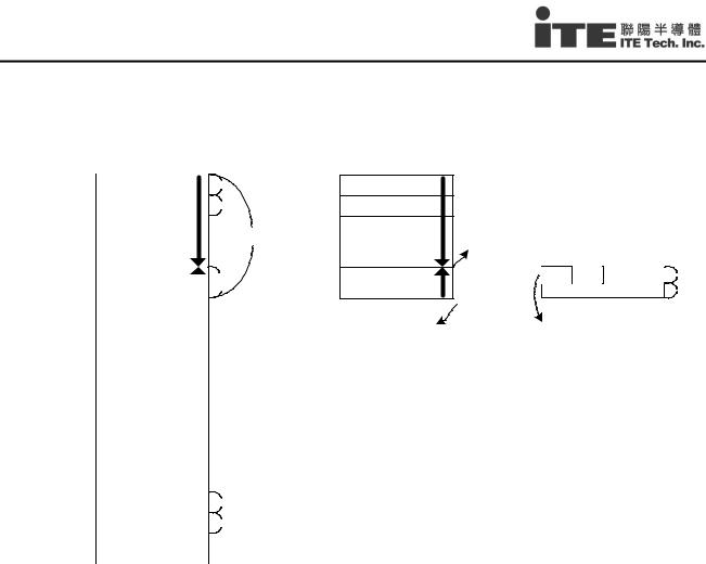
IT8511E/TE/G
3.2Host/EC Mapped Memory Space
Figure 3-1. Host/Flash and EC/Flash Mapping (General)
Host Memory Space
(byte) |
4G Top |
|
FFFF_FFFFh |
||
|
FFFF_0000h |
RANGE 1 |
|||
|
|
|
||
FFFE_FFFFh |
RANGE 2 |
|||
FFFE_0000h |
||||
|
|
|
||
FFFD_FFFFh |
RANGE 3 |
|||
|
||||
Variable, not necessary |
|
|
|
|
on 32k boundary |
|
|
|
|
|
RANGE 4 |
|
|
|
1_0000_0000h - Flash_Size |
|
|
|
|
FFFF_FFFFh - Flash_Size |
|
|
|
|
Out of Range
000F_FFFFh |
|
|
|
||
RANGE 1 |
||
000F_0000h |
||
|
||
000E_FFFFh |
RANGE 2 |
|
000E_0000h |
||
|
||
000D_FFFFh |
Out of Range |
|
|
||
0000_0000h |
|
|
|
Expansion Flash Space |
|
|
(byte) |
Flash Space Top |
|
|
Flash_Size - 1 |
||
64k |
RANGE 1 |
||
Flash_Size - 01_0000h |
|||
|
|
||
64k |
Flash_Size - 01_0001h |
RANGE 2 |
|
Flash_Size - 02_0000h |
|||
|
|
||
|
Flash_Size - 02_0001h |
|
|
|
Flash_Size |
RANGE 3 |
|
|
|
||
EC Code: |
Variable, not necessary |
|
|
on 32k boundary |
RANGE 4 |
||
Max 160k |
|
||
|
00_0000h |
|
EC
Code Memory Space
The range 4 shows space used by EC code and five banks are all used.
The interface line will be lower if EC code size is smaller than 160K.
|
(byte) |
|
|
|
|
|
|
Bank 3 (32k) |
FFFFh |
Bank 0 |
Bank 1 |
Bank 2 |
Bank 3 |
32k |
|
Bank 2 (32k) |
8000h |
||||||
|
|
|
|
|
|||
Bank 1 (32k) |
7FFFh |
|
Common Bank |
|
32k |
||
Bank 0 (32k) |
0000h |
|
|
||||
Common Bank (32k) |
|
|
|
|
|
||
These five banks are arragned in order and totally 160K mapped. |
Bank 0, 1, 2 and 3 occupy the same code memory space. |
||
Each bank is always mapped but it is only valid if it is used by EC code. |
Only one of these four banks can be selected at once time. |
||
If EC code size <= 64K, |
Bank 0 |
is valid to be selected. |
It is selected by ECBB or P1 register. |
If EC code size <= 96K, |
Bank 0-1 are valid to be selected. |
|
|
If EC code size <= 128K, |
Bank 0-2 are valid to be selected. |
|
|
If EC code size <= 160K, Bank 0-3 are valid to be selected. If EC code size is not mutiple of 32K, the remainder can be used by host memory.
64k
64k
www.ite.com.tw |
6 |
IT8511E/TE/G V0.4.1 |

System Block Diagram
Figure 3-2. Host/Flash and EC/Flash Mapping (Flash Size = 512k, EC Code = 64k, a specific example)
Host Memory Space
(byte) |
4G Top |
(byte) |
|
FFFF_FFFFh |
07_FFFFh |
||
RANGE 1 |
|||
FFFF_0000h |
64k |
||
|
07_0000h |
||
FFFE_FFFFh |
RANGE 2 |
06_FFFFh |
|
FFFE_0000h |
64k |
||
|
06_0000h |
||
FFFD_FFFFh |
|
05_FFFFh |
|
|
|
||
|
RANGE 3 |
512k |
|
|
|
||
FFF9_0000h |
|
01_0000h |
|
FFF8_FFFFh |
RANGE 4 |
00_FFFFh |
|
|
64k |
||
FFF8_0000h |
|
00_0000h |
|
FFF7_FFFFh |
|
|
Out of Range
000F_FFFFh |
RANGE 1 |
64k |
|
000F_0000h |
|||
|
|
||
000E_FFFFh |
RANGE 2 |
64k |
|
000E_0000h |
|||
|
|
||
000D_FFFFh |
Out of Range |
|
|
|
|
||
0000_0000h |
|
|
Expansion Flash Space |
|
|
EC |
|
|
|
|
Code Memory Space |
|
||
|
|
|
|
||
Flash Space Top |
|
|
|
|
|
RANGE 1 |
|
|
|
|
|
RANGE 2 |
|
|
|
|
|
RANGE 3 |
|
|
|
|
|
|
|
(byte) |
|
|
|
|
Bank 0 (32k) |
FFFFh |
Bank 0 |
32k |
|
RANGE 4 |
8000h |
||||
|
|
||||
Common Bank (32k) |
7FFFh |
Common Bank |
32k |
||
|
|
0000h |
|
|
Bank 1-3 are not valid to be selected and are not shown.
The flash memory space is shared between the host side and EC side, and it is shown in Figure 3-1. An example of 512k flash size, 64k EC code size is shown in Figure 3-2.
The host memory 4G byte top is always mapped into the top of flash space and the host processor fetches the first instruction after reset at FFFF_FFF0h in the host memory, which is 16 bytes below the uppermost flash space.
The bottom of EC code is always mapped into the bottom of flash space and EC R8032TT micro-controller fetches the first instruction after reset at 00_0000h in the EC code memory, which is 1 byte in the lowermost flash space.
The interface line of host memory and EC code is variable and not necessary on 32k boundary.
Table 3-1. Host/Flash Mapping
Host Memory Space |
Mapped |
|
Size |
Mapping |
on LPC Bus (byte) |
Expansion Flash Space (byte) |
|
(byte) |
Condition |
(1_0000_0000h–Flash_Size)~ |
00_0000h~ |
|
Flash_Size |
Always |
FFFF_FFFFh |
(Flash_Size-1) |
|
|
|
000F_0000h ~ |
(Flash_Size-01_0000h)~ |
|
64k |
Always |
000F_FFFFh |
(Flash_Size-1) |
|
|
|
000E_0000h ~ |
(Flash_Size-02_0000h)~ |
|
64k |
BIOSEXTS= |
000E_FFFFh |
(Flash_Size-01_0001h) |
|
|
1 |
Note: The host side can map all |
flash range regardless of EC code space. |
|
|
|
Note: All host mappings are controlled by HBREN bit in HCTRL2R register. |
|
|
||
Note: Flash Size is defined in FMSSR register. |
|
|
||
www.ite.com.tw |
7 |
|
IT8511E/TE/G V0.4.1 |
|

IT8511E/TE/G
Table 3-2. EC/Flash Mapping
|
EC Code |
|
Mapped |
Size |
Mapping |
Bank Selected |
Memory Space (byte) |
Flash Address Range |
(byte |
Conditio |
Condition |
||
|
|
|
(byte) |
) |
n |
|
Bank 3: |
8000h |
~ FFFFh |
02_0000h ~ 02_7FFFh |
32k |
Always |
ECBB=11 |
Bank 2: |
8000h |
~ FFFFh |
01_8000h ~ 01_FFFFh |
32k |
Always |
ECBB=10 |
Bank 1: |
8000h |
~ FFFFh |
01_0000h ~ 01_7FFFh |
32k |
Always |
ECBB=01 |
Bank 0: |
8000h |
~ FFFFh |
00_8000h ~ 00_FFFFh |
32k |
Always |
ECBB=00 |
Common Bank: 0000h ~ 7FFFh |
00_0000h ~ 00_7FFFh |
32k |
Always |
Always |
||
Note: EC code can use the maximum 160k by banking.
Note: All EC code memory space is mapped to both EC and host side at the same time. The EC size is not necessary on 32k boundary.
Note:
Note: If BSO=1, ECBB is replaced with P1 register of 8032. ECBB means ECBB field in FECBSR register.
BSO means BSO bit in FPCFG register.
Table 3-3. Flash Read/Write Protection Controlled by EC Side
Flash Address |
Read Control |
Write Control |
Note |
Range (byte) |
Register Bits |
Register Bits |
|
02_8000h ~ Top |
ORPLA8 in SMECORPR1 |
ORPLA8 in SMECOWPR1 |
Remainder |
02_0000h ~ 02_7FFFh |
ORPLA7 in SMECORPR0 |
ORPLA7 in SMECOWPR0 |
32K bytes |
01_8000h ~ 01_FFFFh |
ORPLA6 in SMECORPR0 |
ORPLA6 in SMECOWPR0 |
32K bytes |
01_0000h ~ 01_7FFFh |
ORPLA5 in SMECORPR0 |
ORPLA5 in SMECOWPR0 |
32K bytes |
00_8000h ~ 00_FFFFh |
ORPLA4 in SMECORPR0 |
ORPLA4 in SMECOWPR0 |
32K bytes |
00_6000h ~ 00_7FFFh |
ORPLA3 in SMECORPR0 |
ORPLA3 in SMECOWPR0 |
8K bytes |
00_4000h ~ 00_5FFFh |
ORPLA2 in SMECORPR0 |
ORPLA2 in SMECOWPR0 |
8K bytes |
00_2000h ~ 00_3FFFh |
ORPLA1 in SMECORPR0 |
ORPLA1 in SMECOWPR0 |
8K bytes |
00_0000h ~ 00_1FFFh |
ORPLA0 in SMECORPR0 |
ORPLA0 in SMECOWPR0 |
8K bytes |
|
|
All ranges are write-control by |
|
|
|
HOSTWA, too. |
|
|
Table 3-4. Trusted ROM Range |
|
Flash Address |
Trusted ROM Range Enable |
Note |
Range (byte) |
|
32K bytes |
02_0000h ~ 02_7FFFh |
TROMRNG7 in TROMR |
|
01_8000h ~ 01_FFFFh |
TROMRNG6 in TROMR |
32K bytes |
01_0000h ~ 01_7FFFh |
TROMRNG5 in TROMR |
32K bytes |
00_8000h ~ 00_FFFFh |
TROMRNG4 in TROMR |
32K bytes |
00_6000h ~ 00_7FFFh |
TROMRNG3 in TROMR |
8K bytes |
00_4000h ~ 00_5FFFh |
TROMRNG2 in TROMR |
8K bytes |
00_2000h ~ 00_3FFFh |
TROMRNG1 in TROMR |
8K bytes |
00_0000h ~ 00_1FFFh |
Always |
8K bytes |
|
|
Trusted ROM is where TMKBC firmware locates. |
|
|
Only Trusted ROM can access Trusted RAM, |
|
|
which is Scratch RAM with asserted Trust Flag |
|
|
(TRSF bit in SCAR0H~SCAR4H registers, |
|
|
respectively). TROMR register can be modified |
|
|
only by Trusted ROM. |
www.ite.com.tw |
8 |
IT8511E/TE/G V0.4.1 |

System Block Diagram
3.3EC Mapped Memory Space
Figure 3-3. EC 8032 Data/Code Memory Map
|
|
EC Internal |
|
|
|
EC External |
|
EC |
|||
|
|
Data Memory Space |
|
|
|
Data Memory Space |
Code Memory Space |
||||
|
|
|
|
|
FFFFh |
|
|
|
|
|
|
|
|
|
|
|
|
|
|
|
|
|
|
|
|
|
|
|
2600h |
|
Reserved |
|
|
|
|
|
|
|
|
|
|
|
|
|
|
|
|
|
|
|
|
|
2500h |
|
DBGR |
|
|
(byte) |
|
|
|
|
|
|
|
|
|
|
|
|
|
|
|
|
|
|
2400h |
|
TMKBC |
|
|
|
|
|
|
|
|
|
|
|
|
|
|
|
|
|
|
|
|
|
2300h |
|
CIR |
|
adjustable |
|
|
|
|
|
|
|
|
|
|
|
|
||
|
|
|
|
|
2200h |
|
BRAM |
|
|
|
|
|
|
|
|
|
|
|
|
|
|
|
|
|
|
|
|
|
2100h |
|
Reserved |
|
|
|
|
|
|
|
|
|
|
|
|
|
|
|
|
|
|
|
|
|
2000h |
|
GCTRL |
|
|
|
|
|
|
|
|
|
|
|
|
|
|
|
|
|
|
|
|
|
1F00h |
|
ETWD |
|
|
Bank |
|
|
|
|
|
|
|
|
|
|
|
|
|
|
|
|
|
|
1E00h |
|
ECPM |
|
|
0,1,2 or 3 |
|
|
|
|
|
|
|
|
|
|
|
|
|
|
|
|
|
|
1D00h |
|
KB Scan |
|
|
|
|
|
|
|
|
|
|
|
|
|
|
|
|
|
|
|
|
|
1C00h |
|
SM Bus |
|
|
|
|
|
|
|
|
|
|
|
|
|
|
|
|
|
|
|
|
|
1B00h |
|
WUC |
|
|
|
|
|
|
|
|
|
|
|
|
|
|
|
|
|
|
|
|
|
1A00h |
|
DAC |
|
|
|
|
|
|
|
|
|
|
|
|
|
|
|
|
|
|
|
|
|
1900h |
|
ADC |
|
|
|
|
|
|
|
|
|
|
|
|
|
|
|
|
|
|
|
|
|
1800h |
|
PWM |
|
|
|
|
|
|
|
|
|
|
|
|
|
|
|
|
|
|
|
|
|
1700h |
|
PS/2 |
|
Be a RAM or |
|
|
|
|
|
|
|
|
|
|
|
|
|
|
|
|
|
|
|
1600h |
|
GPIO |
|
RAM/ROM |
|
|
|
|
|
|
|
|
|
|
|
|
|
|
|
|
|
|
|
1500h |
|
PMC |
|
|
|
|
|
|
|
|
|
|
|
|
|
|
|
|
|
|
|
|
|
1400h |
|
SWUC |
|
|
|
|
|
|
|
|
|
|
|
|
|
|
|
|
|
|
|
|
|
1300h |
|
KBC |
|
|
|
|
|
|
|
|
|
|
|
|
|
|
|
|
|
|
|
|
|
1200h |
|
EC2I |
|
|
Common |
|
|
|
|
|
|
|
|
|
|
|
|
|
|
|
|
|
|
1100h |
|
INTC |
|
|
Bank |
|
|
|
|
|
|
|
|
|
|
|
|
|
|
|
|
|
|
1000h |
|
SMFI |
|
|
|
|
|
|
|
|
|
|
|
|
|
|
|
|
|
|
|
|
|
0800h |
|
0800h-0FFFh=0000h-07FFh |
|
|
|
|
|
|
|
|
|
|
|
|
|
|
|
|
|
|
|
|
|
0700h |
|
Scratch SRAM No.4 (256B) |
|
|
|
|
|
|
|
|
|
|
|
|
|
|
|
|
FFh |
|
|
|
0600h |
|
Scratch SRAM No.3 (256B) |
|
|
|
|
|
7fh |
|
Indirect |
|
SFR |
0400h |
|
Scratch SRAM No.2 (512B) |
|
|
|
|
00h |
|
Direct & Indirect |
|
|
0000h |
|
Scratch SRAM No.1 (1024B) |
|
|
|
|
|
|
corresponging move |
|
|
|
corresponging read/write |
|
corresponging read |
|||
|
|
instruction: MOV |
|
|
|
instruction: MOVX |
|
instruction: MOVC |
|||
See also Figure 6-3. Scratch SRAM in Data Space on page 65, which also shows Scratch SRAM No 0.
There are five internal Scratch SRAM No 0-4 (No 0 is shared with the same physical SRAM with No 1-4, and is omitted in Figure 3-3. EC 8032 Data/Code Memory Map), which are always mapped into data space and may be mapped into code space if their corresponding code space mapping registers are enabled. It means that Scratch SRAM may be mapped into data and code space at the same time and the firmware on Scratch ROM can access the same Scratch RAM. It is called Scratch RAM when being located at data space (default after reset) and called Scratch ROM when being located at code space.
The EC code space is 64k bytes and physically occupies the maximum 160 k bytes at the bottom of the flash space. Refer to Figure 3-1 on page 6 for the details.
www.ite.com.tw |
9 |
IT8511E/TE/G V0.4.1 |

IT8511E/TE/G
3.4Register Abbreviation
The register abbreviations and access rules are listed below:
R |
READ ONLY. If a register is read only, writing to this register has no effect. |
W |
WRITE ONLY. If a register is write only, reading to this register returns all zero. |
R/W |
READ/WRITE. A register with this attribute can be read and written. |
RC |
READ CLEAR. If a register is read clear, reading to this register clears the register to ‘0’. |
R/WC |
READ/WRITE CLEAR. A register bit with this attribute can be read and written. However, |
|
writing 1 clears the corresponding bit and writing 0 has no effect. |
BFNAME@REGNAME This abbreviation may be shown in figures to represent one bit in a register or one field in a register.
The used radix indicator suffixes in this specification are listed below:
Decimal number: "d" suffix or no suffix
Binary number: "b" suffix
Hexadecimal number: "h" suffix
www.ite.com.tw |
10 |
IT8511E/TE/G V0.4.1 |
Loading...