

PD - 94372C
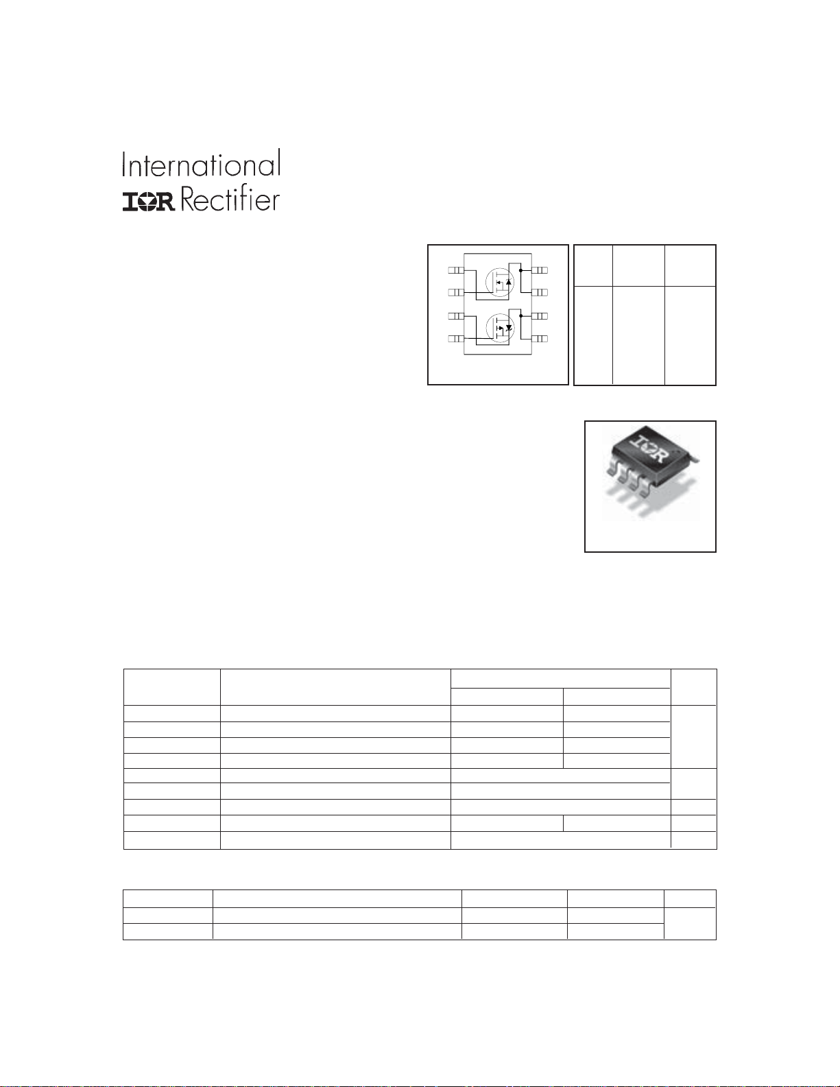
IRF7338
HEXFET® Power MOSFET
l Ultra Low On-Resistance
l Dual N and P Channel MOSFET
l Surface Mount
l Available in Tape & Reel
Description
These N and P channel MOSFETs from International
Rectifier utilize advanced processing techniques to achieve
the extremely low on-resistance per silicon area. This
benefit provides the designer with an extremely efficient
device for use in battery and load management
applications.
This Dual SO-8 has been modified through a customized
leadframe for enhanced thermal characteristics and
multiple-die capability making it ideal in a variety of power
applications. With these improvements, multiple devices
can be used in an application with dramatically reduced
board space. The package is designed for vapor phase,
infrared, or wave soldering techniques.
S1
G1
S2
G2
N-CHANNEL MOSFET
1
2
3
4
P-CHANNEL MOSFET
Top View
8
D1
7
D1
6
5
V
D2
D2
R
N-Ch P-Ch
12V -12V
DSS
0.034Ω 0.150Ω
DS(on)
SO-8
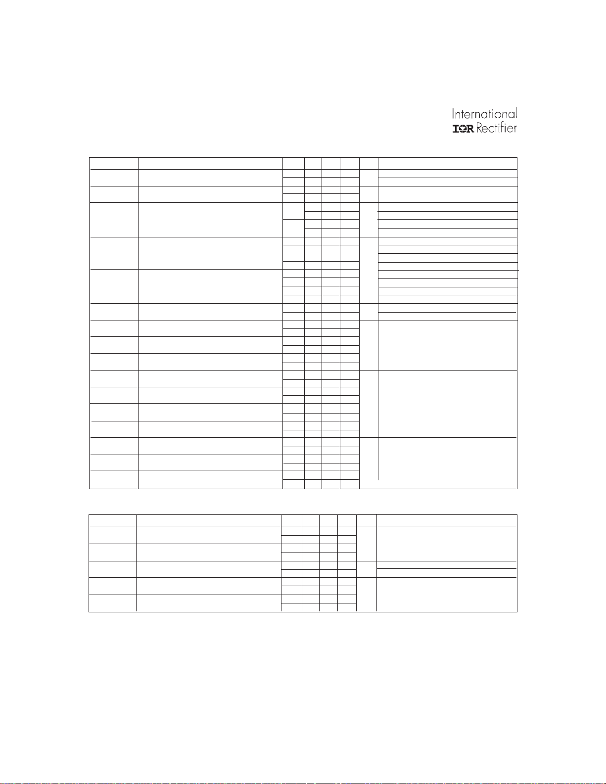
Absolute Maximum Ratings
Parameter
V
DS
ID @ TA = 25°C Continuous Drain Current, VGS @ 4.5V 6.3 -3.0
ID @ TA = 70°C Continuous Drain Current, VGS @ 4.5V 5.2 -2.5
I
DM
PD @TA = 25°C Power Dissipation 2.0 W
PD @TA = 70°C Power Dissipation 1.3
V
GS
T
J, TSTG
Drain-to-Source Voltage 12 -12
Pulsed Drain Current 26 -13
Linear Derating Factor 16 mW/°C
Gate-to-Source Voltage ±12 ± 8.0 V
Junction and Storage Temperature Range °C
N-Channel P-Channel
Max.
-55 to + 150
Units
A
Thermal Resistance
Symbol Parameter Typ. Max. Units
R
θJL
R
θJA
Junction-to-Drain Lead ––– 20
Junction-to-Ambient ––– 62.5 °C/W
www.irf.com 1
6/2/03
IRF7338
Electrical Characteristics @ TJ = 25°C (unless otherwise specified)
V
(BR)DSS
∆V
(BR)DSS
R
DS(ON)
V
GS(th)
g
fs
I
DSS
I
GSS
Q
g
Q
gs
Q
gd
t
d(on)
t
r
t
d(off)
t
f
C
iss
C
oss
C
rss
Drain-to-Source Breakdown Voltage
/∆TJBreakdown Voltage Temp. Coefficient
Static Drain-to-Source On-Resistance
Gate Threshold Voltage
Forward Transconductance
Drain-to-Source Leakage Current
Gate-to-Source Forward Leakage N-Ch –– — ±100 nA VGS = ± 12V
Total Gate Charge
Gate-to-Source Charge
Gate-to-Drain ("Miller") Charge
Turn-On Delay Time
Rise Time
Turn-Off Delay Time
Fall Time
Input Capacitance
Output Capacitance
Reverse Transfer Capacitance
Parameter Min. Typ. Max. Units Conditions
N-Ch 12 — — VGS = 0V, ID = 250µA
P-Ch -12 — — VGS = 0V, ID = -250µA
N-Ch — 0.01 — Reference to 25°C, I
P-Ch — -0.01 — Reference to 25°C, I
— — 0.034 V
N-Ch
— — 0.060 V
— — 0.150 V
P-Ch
— — 0.200 VGS = -2.7V, ID = -1.5A
N-Ch 0.6 — 1.5 V
P-Ch -0.40 — -1.0 V
N-Ch 9.2 — — V
P-Ch 3.5 — — V
N-Ch — — 20 V
P-Ch — — -1.0 VDS = -9.6 V, VGS = 0V
N-Ch — — 50 V
P-Ch — — -25 V
P-Ch — — ±100 V
N-Ch — — 8.6
P-Ch — — 6.6
N-Ch — — 1.9
P-Ch — — 1.3
N-Ch — — 3.9
P-Ch — — 1.6
N-Ch — 6.0 —
P-Ch — 9.6 —
N-Ch — 7.6 —
P-Ch — 13 —
N-Ch — 26 —
P-Ch — 27 —
N-Ch — 34 —
P-Ch — 25 —
N-Ch — 640 —
P-Ch — 490 —
N-Ch — 340 —
P-Ch — 80 —
N-Ch — 110 —
P-Ch — 58 —
V
V/°C
= 4.5V, ID = 6.0A
GS
= 3.0V, ID = 2.0A
GS
Ω
= -4.5V, ID = -2.9A
GS
= VGS, ID = 250µA
DS
V
= VGS, ID = -250µA
DS
= 6.0V, ID = 6.0A
DS
S
= -6.0V, ID = -1.5A
DS
= 9.6V, VGS = 0V
DS
µA
= 9.6V, VGS = 0V, TJ = 55°C
DS
= -9.6V, VGS = 0V, TJ = 55°C
DS
= ± 8.0V
GS
N-Channel
nC
= 6.0A, VDS = 6.0V, VGS = 4.5V
I
D
P-Channel
ID = -2.9A, VDS = -9.6V, VGS = -4.5 V
N-Channel
VDD = 6.0V, ID = 1.0A, RG = 6.0Ω,
ns
V
= 4.5V
GS
P-Channel
V
= -6.0V, ID = -2.9A, RG = 6.0Ω,
DD
VGS = -4.5V
N-Channel
V
pF
= 0V, VDS = 9.0V, ƒ = 1.0MHz
GS
P-Channel
V
= 0V, VDS = -9.0V, ƒ = 1.0KHz
GS
= 1mA
D
= -1mA
D
Source-Drain Ratings and Characteristics
Parameter Min. Typ. Max. Units Conditions
I
S
I
SM
V
SD
t
rr
Q
rr
Continuous Source Current (Body Diode)
Pulsed Source Current (Body Diode)
Diode Forward Voltage
Reverse Recovery Time
Reverse Recovery Charge
Notes:
Repetitive rating; pulse width limited by
max. junction temperature.
Pulse width ≤ 400µs; duty cycle ≤ 2%.
N-Ch — — 6.3
P-Ch — — -3.0
N-Ch — — 26
A
P-Ch — — -13
N-Ch — — 1.3 T
P-Ch — — -1.2 TJ = 25°C, IS = -2.9A, VGS = 0V
N-Ch — 51 76
P-Ch — 37 56
N-Ch — 43 64
P-Ch — 20 30
= 25°C, IS = 1.7A, VGS = 0V
J
V
N-Channel
ns
TJ = 25°C, IF = 1.7A, di/dt = 100A/µs
P-Channel
nC
TJ = 25°C, IF = -2.9A, di/dt = -100A/µs
Surface mounted on 1 in square Cu board.
The N-channel MOSFET can withstand 15V V
for up to 24 hours over the life of the device.
GS
max
2 www.irf.com
N-Channel
IRF7338
100
)
A
(
t
10
n
e
r
r
u
C
e
c
r
1
u
o
S
-
o
t
-
n
i
a
r
0.1
D
,
D
I
1.5V
20µs PULSE WIDTH
0.01
0.1 1 10
Tj = 25°C
VDS, Drain-to-Source Voltage (V)
Fig 1. Typical Output Characteristics
100
VGS
TOP 7 .5 V
4.5V
4.0V
3.5V
3.0V
2.7V
2.0V
BOTTOM 1 .5V
100
)
A
(
t
n
e
r
10
r
u
C
e
c
r
u
o
S
-
o
t
-
1
n
i
a
r
D
,
D
I
VGS
TOP 7 .5V
4.5V
4.0V
3.5V
3.0V
2.7V
2.0V
B OTT OM 1.5V
1.5V
20µs PULSE WIDTH
0.1
0.1 1 10
Tj = 150°C
VDS, Drain-to-Source Voltage (V)
Fig 2. Typical Output Characteristics
100.0
)
A
(
t
n
e
r
r
u
C
e
c
r
10
u
o
S
-
o
t
-
n
i
a
r
D
,
D
I
1
1.0 2.0 3.0 4.0
TJ = 25°C
TJ = 150°C
V
= 10V
DS
20µs PULSE WIDTH
VGS, Gate-to-Source V oltage (V)
Fig 3. Typical Transfer Characteristics
)
A
(
t
n
e
r
r
10.0
u
C
n
i
a
r
D
e
s
r
e
v
1.0
e
R
,
D
S
I
TJ = 150°C
TJ = 25°C
0.1
0.4 0.6 0.8 1.0 1.2 1.4
VSD, Source-toDrain Voltage (V)
Fig 4. Typical Source-Drain Diode
V
= 0V
GS
Forward Voltage
www.irf.com 3
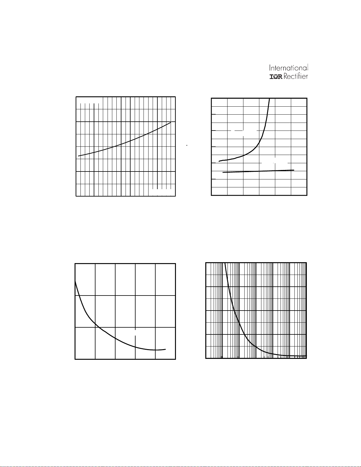
IRF7338
N-Channel
2.0
6.3A
I =
D
1.5
1.0
(Normalized)
0.5
DS(on)
R , Drain-to-Source On Resistance
0.0
-60 -40 -20 0 20 40 60 80 100 120 140 160
T , Junction Temperature ( C)
J
Fig 5. Normalized On-Resistance
Vs. Temperature
)
0.05
Ω
(
e
c
n
a
t
s
i
s
e
R
0.04
n
O
e
c
r
u
o
S
o
t
-
0.03
n
i
a
r
D
,
)
n
o
(
S
D
0.02
R
3.0 4.0 5.0 6.0 7.0 8.0
V
Gate -to -Source Voltage (V)
GS,
ID = 6.3A
V =
GS
°
4.5V
)
0.12
Ω
(
e
c
n
0.10
a
t
s
i
s
e
R
0.08
n
O
e
c
r
0.06
u
o
S
-
o
t
-
n
0.04
i
a
r
D
,
)
0.02
n
o
(
S
D
0.00
R
V
= 3.0V
GS
V
= 4.5V
GS
0 5 10 15 20 25 30
ID , Drain Current (A)
Fig 6. Typical On-Resistance Vs. Drain
Current
80
60
)
W
(
r
40
e
w
o
P
20
0
0.00 0.00 0.00 0.01 0.10 1.00 10.00
Ti me (sec)
Fig 7. Typical On-Resistance Vs. Gate
Fig 8. Typical Power Vs. Time
Voltage
4 www.irf.com

N-Channel
IRF7338
1000
800
)
F
p
(
600
e
c
n
a
t
i
c
a
p
400
a
C
,
C
200
0
Coss
Crss
1 10 100
Ciss
V
= 0V, f = 1 MHZ
GS
C
= C
iss
SHORTED
C
= C
rss
oss
= C
gd
ds
C
+ Cgd, C
gs
+ C
gd
ds
VDS, Drain-to-Source Voltage (V)
Fig 9. Typical Capacitance Vs.
Drain-to-Source Voltage
100
12
ID= 6.0A
)
V
10
(
e
g
a
t
l
8
o
V
e
c
r
u
6
o
S
-
o
t
-
e
t
4
a
G
,
S
2
G
V
VDS= 12V
0
0.0 2.0 4.0 6.0 8.0 10.0 12.0
Q
Total Gate Charge (nC)
G
Fig 10. Typical Gate Charge Vs.
Gate-to-Source Voltage
D = 0.50
thJA
Thermal Response (Z )
0.20
10
0.10
0.05
0.02
0.01
1
0.1
0.00001 0.0001 0.001 0.01 0.1 1 10
SINGLE PULSE
(THERMAL RESPONSE)
t , Rectangular Pulse Duration (sec)
1
Notes:
1. Duty factor D = t / t
2. Peak T = P x Z + T
J DM thJA A
1 2
P
DM
t
1
t
2
Fig 11. Maximum Effective Transient Thermal Impedance, Junction-to-Ambient
www.irf.com 5

IRF7338
N-Channel
7.0
6.0
5.0
4.0
3.0
D
I , Drain Current (A)
2.0
1.0
0.0
25 50 75 100 125 150
T , Case Temperature ( C)
C
°
Fig 12. Maximum Drain Current Vs.
Case Temperature
R
V
DS
V
GS
R
G
V
GS
Pulse Width ≤ 1 µs
Duty Factor ≤ 0.1 %
D
D.U.T.
Fig 13a. Switching Time Test Circuit
V
DS
90%
10%
V
GS
t
d(on)tr
t
d(off)tf
Fig 13b. Switching Time Waveforms
+
V
DD
-
Current Regulator
Same Type as D.U.T.
Q
G
V
GS
Q
GS
V
G
Q
GD
Charge
Fig 14a. Basic Gate Charge Waveform
12V
V
GS
Fig 14b. Gate Charge Test Circuit
50KΩ
.2µF
.3µF
3mA
Current Sampling Resistors
+
V
D.U.T.
I
G
DS
-
I
D
6 www.irf.com

P-Channel
IRF7338
100
)
A
(
t
n
e
r
r
10
u
C
e
c
r
u
o
S
-
o
t
-
n
1
i
a
r
D
,
D
I
-
0.1
0.1 1 10
VGS
TOP -7.5V
-4.5V
-4.0V
-3.5V
-3.0V
-2.7V
-2.0V
BOTTOM -1.5V
-1.5V
20µs PULSE W IDTH
Tj = 25°C
-VDS, Drain-to-Source Voltage (V)
Fig 15. Typical Output Characteristics
100
100
)
A
(
t
n
e
r
r
10
u
C
e
c
r
u
o
S
-
o
t
-
n
1
i
a
r
D
,
D
I
-
0.1
0.1 1 10
VGS
TOP -7.5V
-4.5V
-4.0V
-3.5V
-3.0V
-2.7V
-2.0V
BOTTOM - 1.5V
-1.5V
20µs PULSE W IDTH
Tj = 150°C
-VDS, Drain-to-Source Voltage (V)
Fig 16. Typical Output Characteristics
100.0
)
A
(
t
n
e
r
r
u
C
e
c
r
10
u
o
S
-
o
t
-
n
i
a
r
D
,
D
I
-
1
TJ = 25°C
TJ = 150°C
V
= - 10V
DS
20µs PULSE WIDTH
1.0 2.0 3.0 4.0
-VGS, Gate-to-Source Voltage (V)
Fig 17. Typical Transfer Characteristics
)
A
(
t
n
e
r
r
10.0
u
C
n
i
a
r
D
e
s
r
e
v
e
R
,
D
S
I
-
TJ = 150°C
1.0
TJ = 25°C
0.1
0.4 0.6 0.8 1.0 1.2 1.4 1.6
-VSD, Source-toDrain Voltage (V)
Fig 18. Typical Source-Drain Diode
V
= 0V
GS
Forward Voltage
www.irf.com 7

IRF7338
2.0
-3.0A
I =
D
1.5
1.0
(Normalized)
0.5
DS(on)
R , Drain-to-Source On Resistance
0.0
-60 -40 -20 0 20 40 60 80 100 120 140 160
T , Junction Temperature ( C)
J
V =
GS
°
-4.5V
P-Channel
)
Ω
(
e
c
n
a
t
s
i
s
e
R
n
O
e
c
r
u
o
S
-
o
t
-
n
i
a
r
D
,
)
n
o
(
S
D
R
0.20
0.18
0.16
0.14
V
= -2.7V
GS
0.12
0.10
V
= -4.5V
GS
0.08
0.06
02468101214
-ID , Drain Current (A)
Fig 19. Normalized On-Resistance
Vs. Temperature
)
0.12
Ω
(
e
c
n
a
t
s
i
s
e
R
0.10
n
O
e
c
r
u
o
S
o
t
-
0.08
n
i
a
r
D
,
)
n
o
(
S
D
0.06
R
2.0 3.0 4.0 5.0 6.0 7.0 8.0
-V
Gate -to -Source Voltage (V)
GS,
ID = -3.0A
Fig 21. Typical On-Resistance Vs. Gate
Voltage
Fig 20. Typical On-Resistance Vs. Drain
Current
80
60
)
W
(
r
40
e
w
o
P
20
0
0.00 0.00 0.00 0.01 0.10 1.00 10.00
Ti me (sec)
Fig 22. Maximum Avalanche Energy
Vs. Drain Current
8 www.irf.com

P-Channel
IRF7338
800
600
)
F
p
(
e
c
n
a
t
400
i
c
a
p
a
C
,
C
200
Ciss
Coss
V
= 0V, f = 1 MHZ
GS
C
= C
iss
SHORTED
C
= C
rss
oss
= C
gd
ds
C
+ Cgd, C
gs
+ C
gd
ds
Crss
0
1 10 100
-VDS, Drain-to-Source Voltage (V)
-
Fig 23. Typical Capacitance Vs.
Drain-to-Source Voltage
100
12
ID= -2.9A
)
V
10
(
e
g
a
t
l
o
8
V
e
c
r
u
6
o
S
-
o
t
-
e
t
4
a
G
,
S
G
2
V
-
VDS= -9.6V
VDS= -6.0V
0
0246810
Q
Total Gate Charge (nC)
G
Fig 24. Typical Gate Charge Vs.
Gate-to-Source Voltage
D = 0.50
thJA
Thermal Response (Z )
0.20
10
0.10
0.05
0.02
0.01
1
0.1
0.00001 0.0001 0.001 0.01 0.1 1 10
SINGLE PULSE
(THERMAL RESPONSE)
t , Rectangular Pulse Duration (sec)
1
Notes:
1. Duty factor D = t / t
2. Peak T = P x Z + T
J DM thJA A
1 2
P
DM
t
1
t
2
Fig 25. Maximum Effective Transient Thermal Impedance, Junction-to-Ambient
www.irf.com 9

IRF7338
3.0
2.4
1.8
1.2
D
-I , Drain Current (A)
0.6
0.0
25 50 75 100 125 150
T , Case Tempe ra ture ( C)
C
°
Fig 26. Maximum Drain Current Vs.
Case Temperature
R
D.U.T.
D
-
+
V
V
DS
V
GS
R
G
V
GS
Pulse Width ≤ 1 µs
Duty Factor ≤ 0.1 %
Fig 27a. Switching Time Test Circuit
V
GS
10%
90%
V
DS
t
d(on)tr
t
d(off)tf
Fig 27b. Switching Time Waveforms
DD
Current Regulator
Same Type as D.U.T.
50KΩ
Q
G
Q
GS
V
G
Q
GD
Charge
Fig 28a. Basic Gate Charge Waveform
Fig 28b. Gate Charge Test Circuit
12V
.2µF
V
GS
.3µF
D.U.T.
-3mA
I
G
Current Sampling Resistors
V
DS
+
I
D
10 www.irf.com

SO-8 Package Details
IRF7338
D B
8X b
5
65
4312
e1
CAB
A1
H
0.25 [.010] A
A
C
0.10 [.004]
A
87
6
E
e
6X
0.25 [.010]
NOTE S:
1. DIMENSIONING & TOLER ANCING PER ASME Y14.5M-1994.
2. CONTROLLING DIMENSION: MILLIMETER
3. DIME NS IONS ARE S HOWN IN MILL IMET E R S [INCHE S].
4. OUT LINE CONFORMS T O JEDE C OUT LINE MS-012AA.
5 DIMENS ION DOES NOT INCLUDE MOLD PR OTR USIONS .
MOLD PR OTR US IONS NOT T O EXCEED 0.15 [.006].
6 DIMENS ION DOES NOT INCLUDE MOLD PR OTR USIONS .
MOLD PR OTR US IONS NOT T O EXCEED 0.25 [.010].
7 DIMENS ION IS T HE L ENGTH OF L EAD FOR S OLDE R ING T O
A SU BS T RATE.
y
3X 1.27 [.050]
DIM
MI N MAX
A
.0532
A1
b
c .0075 .0098 0.19 0.25
D
E
e
e1
H
K
L
y
K x 45°
8X L
7
6.46 [.255]
.0688
.0040
.0098
.013
.020
.189
.1968
.1497
.1574
.050 BASI C
.025 BASIC 0.635 BAS IC
.2284
.2440
.0099
.0196
.016
.050
0°
8°
8X c
F OOT P R I NT
8X 0.72 [.028]
MI LL I ME T E R SINCHES
MI N MAX
1.35
1.75
0.10
0.25
0.33
0.51
4.80
5.00
3.80
4.00
1.27 BASI C
5.80
6.20
0.25
0.50
0.40
1.27
8°
0°
8X 1.78 [.070]
SO-8 Part Marking
EXAMPLE : T HIS IS AN IRF 7101 (MOSF ET )
DAT E CODE (YWW)
Y = LAS T DIGIT OF THE YEAR
YWW
XXXX
INTERNATIONAL
F7101
RECTIF IER
LOGO
www.irf.com 11
WW = WE E K
LOT CODE
PART NUMBER

IRF7338
SO-8 Tape and Reel
TERMINAL NUMBER 1
12.3 ( .484 )
11.7 ( .461 )
8.1 ( .318 )
7.9 ( .312 )
NOTES:
1. CONTROLLING DIMENSION : MILLIMETER.
2. ALL DIMENSIONS ARE SHOWN IN MILLIMETERS(INCHES).
3. OUTLINE CONFORMS TO EIA-481 & EIA-541.
330.00
(12.992)
MAX.
NOTES :
1. CONTROLLING DIMENSION : MILLIMETER.
2. OUTLINE CONFORMS TO EIA-481 & EIA-541.
Data and specifications subject to change without notice.
This product has been designed and qualified for the Consumer market.
Qualification Standards can be found on IR’s Web site.
FEED DIRECTION
14.40 ( .566 )
12.40 ( .488 )
IR WORLD HEADQUARTERS: 233 Kansas St., El Segundo, California 90245, USA Tel: (310) 252-7105
TAC Fax: (310) 252-7903
Visit us at www.irf.com for sales contact information.6/03
12 www.irf.com
 Loading...