

D
D
K
K
查询IRF7321D2PBF供应商
l Co-packaged HEXFET® Power
MOSFET and Schottky Diode
l Ideal For Buck Regulator Applications
l P-Channel HEXFET®
l Low V
l Generation 5 Technology
l SO-8 Footprint
l Lead-Free
Description
The FETKYTM family of Co-packaged HEXFETs and
Schottky diodes offer the designer an innovative board
space saving solution for switching regulator and
power management applications. Generation 5
HEXFETs utilize advanced processing techniques to
achieve extremely low on-resistance per silicon area.
Combinining this technology with International
Rectifier's low forward drop Schottky rectifiers results in
an extremely efficient device suitable for use in a wide
variety of portable electronics applications.
The SO-8 has been modified through a customized
leadframe for enhanced thermal characteristics. The
SO-8 package is designed for vapor phase, infrared or
wave soldering techniques.
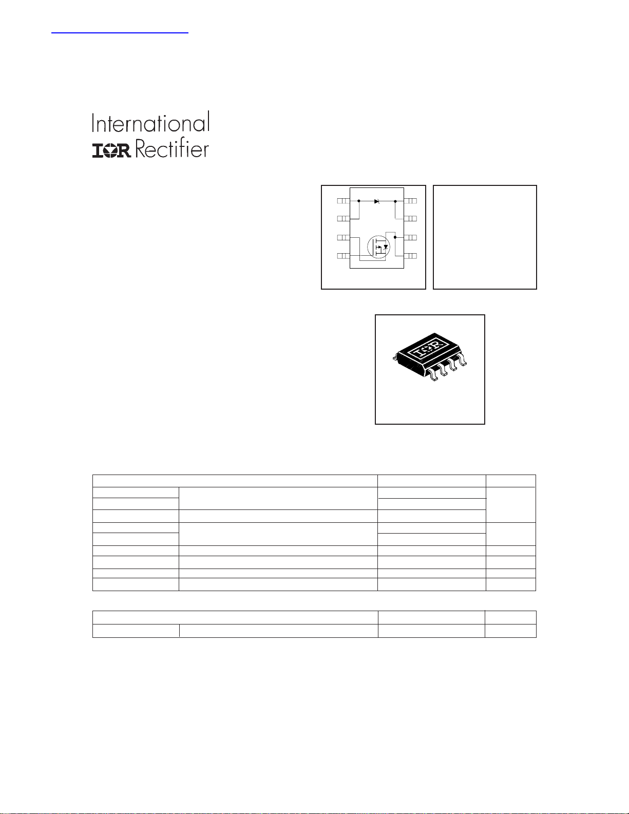
Schottky Rectifier
F
PD - 95297
IRF7321D2PbF
FETKY MOSFET & Schottky Diode
A
A
S
G
TM
1
2
3
4
Top View
8
7
6
5
V
= -30V
DSS
R
DS(on)
= 0.062Ω
Schottky Vf = 0.52V
SO-8
Absolute Maximum Ratings ( TA = 25°C Unless Otherwise Noted)
Parameter Maximum Units
ID @ TA = 25°C Continuous Drain Current, VGS @ -10V -4.7 A
ID @ TA = 70°C -3.8
I
DM
PD @TA = 25°C Power Dissipation 2.0 W
PD @TA = 70°C 1.3
V
GS
dv/dt Peak Diode Recovery dv/dt Á -5.0 V/ns
T
J, TSTG
Pulsed Drain Current À -38
Linear Derating Factor 16 mW/°C
Gate-to-Source Voltage ± 20 V
Junction and Storage Temperature Range -55 to +150 °C
Thermal Resistance Ratings
Parameter Maximum Units
R
θJA
Notes:
Junction-to-Ambient à 62.5 °C/W
Repetitive rating – pulse width limited by max. junction temperature (see fig. 11)
I
≤ -2.9A, di/dt ≤ -77A/µs, V
SD
DD
≤ V
(BR)DSS
, TJ ≤ 150°C
Pulse width ≤ 300µs – duty cycle ≤ 2%
Surface mounted on FR-4 board, t ≤ 10sec.
www.irf.com
10/12/04
IRF7321D2PbF
MOSFET Electrical Characteristics @ TJ = 25°C (unless otherwise specified)
Parameter Min. Typ. Max. Units Conditions
V
(BR)DSS
R
DS(on)
V
GS(th)
g
fs
I
DSS
I
GSS
Q
g
Q
gs
Q
gd
t
d(on)
t
r
t
d(off)
t
f
C
iss
C
oss
C
rss
MOSFET Source-Drain Ratings and Characteristics
I
S
I
SM
V
SD
t
rr
Q
rr
Schottky Diode Maximum Ratings
If (av) Max. Average Forward Current 3.2 50% Duty Cycle. Rectangular Wave, Tc = 25°C
I
SM
Schottky Diode Electrical Specifications
Vfm Max. Forward voltage drop 0.57 If = 3.0, Tj = 25°C
Irm Max. Reverse Leakage current 0.30 Vr = 30V Tj = 25°C
Ct Max. Junction Capacitance 310 pF Vr = 5Vdc ( 100kHz to 1 MHz) 25°C
dv/dt Max. Voltage Rate of Charge 4900 V/µs Rated Vr
( HEXFET is the reg. TM for International Rectifier Power MOSFET's )
2 www.irf.com
Drain-to-Source Breakdown Voltage -30 ––– ––– V VGS = 0V, ID = -250µA
Static Drain-to-Source On-Resistance
––– 0.042 0.062 VGS = -10V, ID = -4.9A
––– 0.076 0.098 V
Ω
= -4.5V, ID = -3.6A
GS
Gate Threshold Voltage -1.0 ––– ––– V VDS = VGS, ID = -250µA
Forward Transconductance ––– 7.7 ––– S VDS = -15V, ID = -4.9A
Drain-to-Source Leakage Current
Gate-to-Source Forward Leakage ––– ––– 100 VGS = -20V
Gate-to-Source Reverse Leakage ––– ––– -100 VGS = 20V
––– ––– -1.0 V
––– ––– -25 VDS = -24V, VGS = 0V, TJ = 55°C
µA
nA
= -24V, VGS = 0V
DS
Total Gate Charge ––– 23 34 ID = -4.9A
Gate-to-Source Charge ––– 3.8 5.7 nC VDS = -15V
Gate-to-Drain ("Miller") Charge ––– 5.9 8.9 VGS = -10V, See Fig. 6
Turn-On Delay Time ––– 13 19 VDD = -15V
Rise Time ––– 13 20 ID = -1.0A
Turn-Off Delay Time ––– 34 51 RG = 6.0Ω
ns
Fall Time ––– 32 48 RD = 15Ω,
Input Capacitance ––– 710 ––– VGS = 0V
Output Capacitance ––– 380 ––– pF VDS = -25V
Reverse Transfer Capacitance ––– 180 ––– ƒ = 1.0MHz, See Fig. 5
Parameter Min. Typ. Max. Units Conditions
Continuous Source Current(Body Diode) ––– ––– -2.5
Pulsed Source Current (Body Diode) ––– ––– -30
A
Body Diode Forward Voltage ––– -0.78 -1.0 V TJ = 25°C, IS = -1.7A, VGS = 0V
Reverse Recovery Time (Body Diode) ––– 44 66 ns TJ = 25°C, IF = -1.7A
Reverse Recovery Charge ––– 42 63 nC di/dt = 100A/µs
Parameter Max. Units Conditions
A
2.0 See Fig.14 Tc = 70°C
Max. peak one cycle Non-repetitive 200 5µs sine or 3µs Rect. pulse Following any rated
Surge current 20 10ms sine or 6ms Rect. pulse load condition &
A
with Vrrm applied
Parameter Max. Units Conditions
0.77 If = 6.0, Tj = 25°C
V
0.52 If = 3.0, Tj = 125°C
0.79 If = 6.0, Tj = 125°C .
mA
37 Tj = 125°C
A
A
A
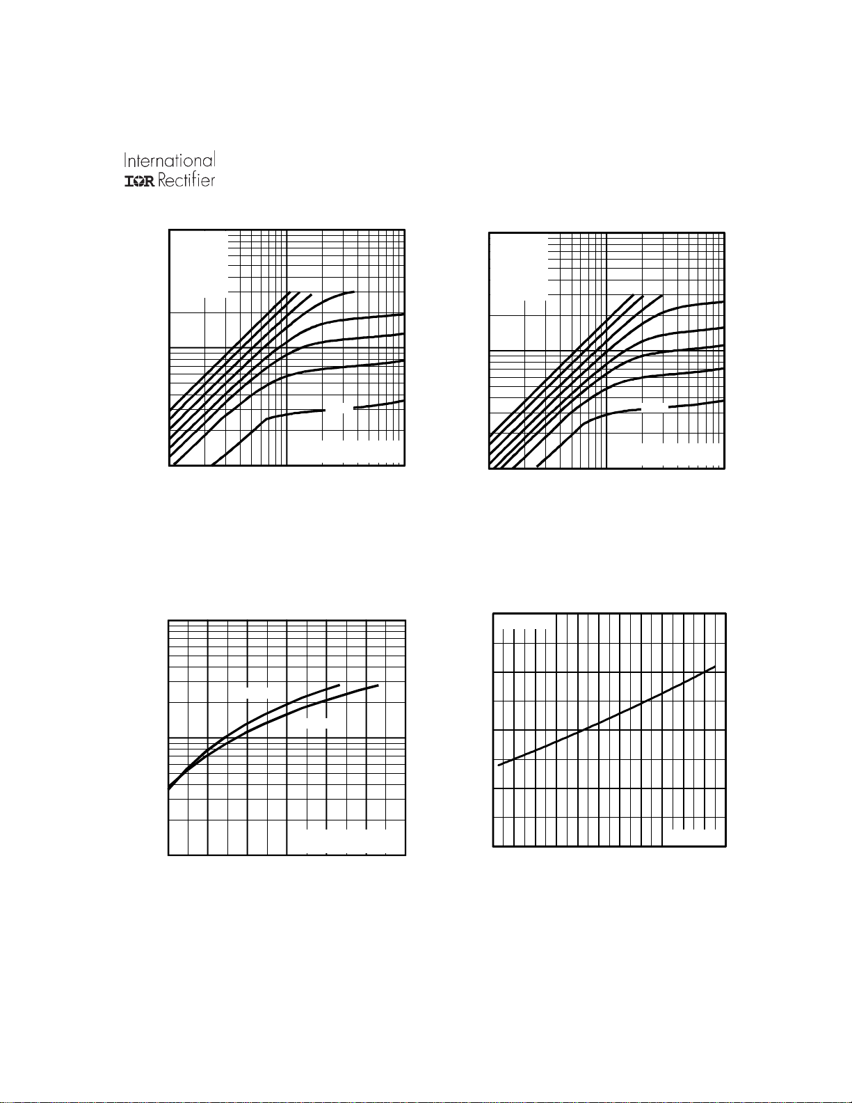
Power Mosfet Characteristics
IRF7321D2PbF
100
VGS
TOP - 15V
- 10V
- 7.0V
- 5.5V
- 4.5V
- 4.0V
- 3.5V
BOTTOM - 3.0V
10
-3.0V
D
-I , Drain-to-Source Current (A)
20µs PULSE WIDTH
T = 25°C
1
0.1 1 10
-V , Drain-to-Source Voltage (V)
DS
100
J
100
VGS
TOP - 15V
- 10V
- 7.0V
- 5.5V
- 4.5V
- 4.0V
- 3.5V
BOTTOM - 3.0V
10
-3.0V
D
-I , Drain-to-Source Current (A)
20µs PULSE WIDTH
T = 150°C
1
0.1 1 10
-V , Drain-to-Source Voltage (V)
DS
J
Fig 2. Typical Output CharacteristicsFig 1. Typical Output Characteristics
2.0
---4.9A
4.9A
I =
D
1.5
T = 25°C
J
T = 150°C
10
J
1.0
(Normalized)
0.5
D
-I , Drain-to-Source Current (A)
1
3.0 3.5 4.0 4.5 5.0 5.5 6.0
-V , Gate-to-Source Voltage (V)
GS
V = -10V
DS
20µs PULSE WIDTH
DS(on)
R , Drain-to-Source On Resistance
0.0
-60 -40 -20 0 20 40 60 80 100 120 140 160
T , Junction Temperature ( C)
J
V =
GS
°
-10V
10V
Fig 4. Normalized On-Resistance
Fig 3. Typical Transfer Characteristics
Vs. Temperature
www.irf.com 3

IRF7321D2PbF
A
A
Power Mosfet Characteristics
1400
1200
1000
800
600
C, Capacitance (pF)
400
200
0
1 10 100
VGS = 0V f = 1 MHz
Ciss = Cgs + Cgd + Cds SHORTED
Crss = Cgd
Coss = Cds + Cgd
C
iss
C
oss
C
rss
-
V , Drain-to-Source Voltage (V)
DS
Fig 5. Typical Capacitance Vs.
Drain-to-Source Voltage
100
20
I =D-4.9A
V =-15V
DS
16
12
8
4
GS
-V , Gate-to-Source Voltage (V)
0
0 10 20 30 40
Q , Total Gate Charge (nC)
G
Fig 6. Typical Gate Charge Vs.
Gate-to-Source Voltage
100
OPERATION IN THIS AREA LIMITED
BY R
DS(on)
T = 150°C
J
10
T = 25°C
J
SD
-I , Reverse Drain Current (A)
1
0.4 0.6 0.8 1.0 1.2 1.4
-V , Source-to-Drain Voltage (V)
SD
V = 0V
Fig 7. Typical Source-Drain Diode
Forward Voltage
GS
10
D
-I , Drain Current (A)I , Drain Current (A)
°
= 25 C
C
T T= 150 C
Single Pulse
1
1 10 100
°
J
-V , Drain-to-Source Voltage (V)
DS
Fig 8. Maximum Safe Operating Area
100us
1ms
10ms
4 www.irf.com

100
A
A
thJA
10
IRF7321D2PbF
Power Mosfet Characteristics
0.50
0.20
0.10
0.05
0.02
1
0.01
Thermal Response (Z )
SINGLE PULSE
(THERMAL RESPONSE)
0.1
0.00001 0.0001 0.001 0.01 0.1 1 10 100
t , Rectangular Pulse Duration (sec)
1
Notes:
1. Duty factor D = t / t
2. Peak T =P x Z + T
J DM thJA A
1 2
P
DM
t
1
t
2
Fig 9. Maximum Effective Transient Thermal Impedance, Junction-to-Ambient
0.6
0.5
0.4
0.3
V = -4.5V
0.2
0.1
(on) , Drain-to-Source On Resistance (Ω)
DS
R
0.0
0 102030
GS
V = -10V
GS
-ID , Drain Current (A)
0.16
0.12
0.08
0.04
I = -4.9A
D
(on) , Drain-to-Source On Resistance (Ω)
DS
R
0.00
0 3 6 9 12 15
-VGS , Gate -to-Source Voltage (V)
Fig 10. Typical On-Resistance Vs. Drain
Current
Fig 11. Typical On-Resistance Vs. Gate
Voltage
www.irf.com 5

IRF7321D2PbF
A
)
Schottky Diode Characteristics
100
10
F
T = 150°C
T = 125°C
T = 25°C
1
Instantaneous Forward Current - I (A)
0.1
0.0 0.2 0.4 0.6 0.8 1.0
Forward Voltage Drop - V (V)
Forward Voltage Drop - VF (V)
Fig. 12 - Typical Forward Voltage Drop
Characteristics
100
J
10
(mA)
1
R
0.1
0.01
J
J
J
Reverse Current - I
0.001
0102030
R
)
Fig. 13 - Typical Values of
Reverse Current Vs. Reverse Voltage
FM
160
140
120
100
80
60
D = 3/4
D = 1/2
40
D =1/3
D = 1/4
20
D = 1/5
Allowable Ambient Temperature - (°C
0
0.0 0.5 1.0 1.5 2.0 2.5 3.0 3.5 4.0
Average Forward Current - I (A)
V = 80% Rated
r
R = 62.5°C/W
thJA
Square wave
DC
F(AV)
Fig.14 - Maximum Allowable Ambient
Temp. Vs. Forward Current
6 www.irf.com

SO-8 (Fetky) Package Outline
IRF7321D2PbF
D B
8X b
5
65
4312
e1
CAB
A1
H
0.25 [.0 10] A
A
C
0.10 [.00 4]
A
87
6
E
e
6X
0.25 [.010 ]
NOTE S :
1. DIMENS IONING & T OLERANCING PER ASME Y14.5M-1994.
2. CONT ROL LING DIME NS ION: MI L LIME T E R
3. DIMENS IONS AR E SHOWN IN MILL IMETER S [INCHES ].
4. OUTLINE CONFORMS TO JEDEC OUTLINE MS-012AA.
5 DIMENS ION DOE S NOT INCL UDE MOLD P ROTRU S IONS .
MOLD PROTR US IONS NOT TO EXCEE D 0.15 [.006].
6 DIMENS ION DOE S NOT INCL UDE MOLD P ROTRU S IONS .
MOLD PROTR US IONS NOT TO EXCEE D 0.25 [.010].
7 DIMENS ION IS T HE LENGTH OF L EAD FOR S OL DE RING TO
A S UB ST RATE .
y
DIM
A
A1
b
c .0075 .0098 0.19 0.25
D
E
e
e1
H
K
L
y
K x 45°
8X L
7
6.46 [.255]
3X 1.27 [.050]
MIN MAX
.0532
.0040
.013
.189
.1497
.050 BAS IC
.025 BAS IC 0.635 B AS IC
.2284
.0099
.016
0°
8X c
MI L L I ME T E R SINCHE S
MIN MAX
1.35
.0688
0.10
.0098
0.33
.020
4.80
.1968
3.80
.1574
1.27 B AS IC
5.80
.2440
0.25
.0196
0.40
.050
0°
8°
FOOTPRINT
8X 0.72 [.028]
1.75
0.25
0.51
5.00
4.00
6.20
0.50
1.27
8°
8X 1.78 [.070]
SO-8 (Fetky) Part Marking Information
EXAMPLE: T HIS IS AN IRF 7807D1 (FE T KY)
XXXX
INTE RNAT IONAL
807D1
RECT IF IER
LOGO
www.irf.com 7
DATE CODE (YWW)
P = DISGNATES LEAD - FREE
PRODUCT (OPTIONAL)
Y = L AS T DIGIT OF T HE YEAR
WW = WE E K
A = ASSEMBLY SITE CODE
LOT CODE
PART NUMBER

IRF7321D2PbF
SO-8 Tape and Reel
Dimensions are shown in milimeters (inches)
TERMINAL NUMBER 1
12.3 ( .484 )
11.7 ( .461 )
8.1 ( .318 )
7.9 ( .312 )
NOTES:
1. CONT ROLLING DIM ENSION : MIL LIMETER.
2. ALL DIMENS IONS ARE SHOWN IN MILL IME TER S(INCHES).
3. OUTLINE CONFORMS TO EIA-481 & EIA-541.
330.00
(12.992)
MAX.
NOTES :
1. CO NTROLLING DIMENSION : MILLIMETER.
2. OUTLINE CO NFORMS TO EIA-481 & EIA-541.
FEED DIRECTION
14.40 ( . 566 )
12.40 ( . 488 )
Data and specifications subject to change without notice.
This product has been designed and qualified for the Consumer market.
Qualifications Standards can be found on IR’s Web site.
IR WORLD HEADQUARTERS: 233 Kansas St., El Segundo, California 90245, USA Tel: (310) 252-7105
TAC Fax: (310) 252-7903
Visit us at www.irf.com for sales contact information.10/04
8 www.irf.com
 Loading...