

HEXFET® Power MOSFET
Next Data SheetIndex
Previous Datasheet
To Order
Advanced Process Technology
Ultra Low On-Resistance
Surface Mount
Available in Tape & Reel
Dynamic dv/dt Rating
Repetitive Avalanche Rated
175°C Operating Temperature
Description
Fourth Generation HEXFETs from International Rectifier utilize advanced
processing techniques to achieve the lowest possible on-resistance per silicon
area. This benefit, combined with the fast switching speed and ruggedized device
design that HEXFET Power MOSFETs are well known for, provides the designer
with an extremely efficient device for use in a wide variety of applications.
The SMD-220 is a surface mount power package capable of accommodating die
sizes up to HEX-4. It provides the highest power capability and the lowest possible
on-resistance in any existing surface mount package. The SMD-220 is suitable for
high current applications because of its low internal connection resistance and can
dissipate up to 2.0W in a typical surface mount application.
PD - 9.1221
IRF1310S
V
= 100V
DSS
R
ID = 41A
DS(on)
SMD-220
= 0.04Ω
Absolute Maximum Ratings
Parameter Max. Units
ID @ TC = 25°C Continuous Drain Current, VGS @ 10V 41
ID @ TC = 100°C Continuous Drain Current, VGS @ 10V 29 A
I
DM
PD @TC = 25°C Power Dissipation 170
PD @TC = 25°C Power Dissipation (PCB Mount)** 3.8
V
GS
E
AS
I
AR
E
AR
dv/dt Peak Diode Recovery dv/dt 5.5 V/ns
T
J, TSTG
Pulsed Drain Current 160
Linear Derating Factor 1.1
Linear Derating Factor (PCB Mount)** 0.025
Gate-to-Source Voltage ±20 V
Single Pulse Avalanche Energy 230 mJ
Avalanche Current 41 A
Repetitive Avalanche Energy 17 mJ
Junction and Storage Temperature Range -55 to + 175
Soldering Temperature, for 10 seconds 300 (1.6mm from case)
W/°C
Thermal Resistance
Parameter Min. Typ. Max. Units
R
θJC
R
θJA
R
θJA
** When mounted on 1" square PCB (FR-4 or G-10 Material).
For recommended footprint and soldering techniques refer to application note #AN-994.
Junction-to-Case –––– –––– 0.90
Junction-to-Ambient (PCB Mount)** –––– –––– 40 °C/W
Junction-to-Ambient –––– –––– 62
W
°C
Revision 0
IRF1310S
Next Data SheetIndex
Previous Datasheet
To Order
Electrical Characteristics @ TJ = 25°C (unless otherwise specified)
Parameter Min. Typ. Max. Units Conditions
V
(BR)DSS
∆V
(BR)DSS
R
DS(ON)
V
GS(th)
g
fs
I
DSS
I
GSS
Q
g
Q
gs
Q
gd
t
d(on)
t
r
t
d(off)
t
f
L
D
L
S
C
iss
C
oss
C
rss
Drain-to-Source Breakdown Voltage 100 ––– ––– V VGS = 0V, ID = 250µA
/∆T
Breakdown Voltage Temp. Coefficient ––– 0.10 ––– V/°C Reference to 25°C, ID = 1mA
J
Static Drain-to-Source On-Resistance ––– ––– 0.04 Ω VGS = 10V, ID = 25A
Gate Threshold Voltage 2.0 ––– 4.0 V VDS = VGS, ID = 250µA
Forward Transconductance 12 ––– ––– S VDS = 50V, ID = 25A
Drain-to-Source Leakage Current
Gate-to-Source Forward Leakage ––– ––– 100 VGS = 20V
Gate-to-Source Reverse Leakage ––– ––– -100 VGS = -20V
––– ––– 25 VDS = 100V, VGS = 0V
––– ––– 250 VDS = 80V, VGS = 0V, TJ = 150°C
µA
nA
Total Gate Charge ––– ––– 110 ID = 25A
Gate-to-Source Charge ––– ––– 18 nC VDS = 80V
Gate-to-Drain ("Miller") Charge ––– ––– 42 VGS = 10V, See Fig. 6 and 13
Turn-On Delay Time ––– 13 ––– VDD = 50V
Rise Time ––– 77 ––– ID = 25A
Turn-Off Delay Time ––– 82 ––– RG = 9.1Ω
ns
Fall Time ––– 64 ––– RD = 2.0Ω, See Fig. 10
Internal Drain Inductance ––– 4.5 –––
Internal Source Inductance ––– 7.5 –––
Between lead,
6mm (0.25in.)
nH
from package
and center of die contact
Input Capacitance ––– 2500 ––– VGS = 0V
Output Capacitance ––– 630 ––– pF VDS = 25V
Reverse Transfer Capacitance ––– 130 ––– ƒ = 1.0MHz, See Fig. 5
Source-Drain Ratings and Characteristics
I
S
I
SM
V
SD
t
rr
Q
rr
t
on
Notes:
Repetitive rating; pulse width limited by
max. junction temperature. ( See fig. 11 )
V
= 25V, starting TJ = 25°C, L = 3.1mH
DD
RG = 25Ω, I
Parameter Min. Typ. Max. Units Conditions
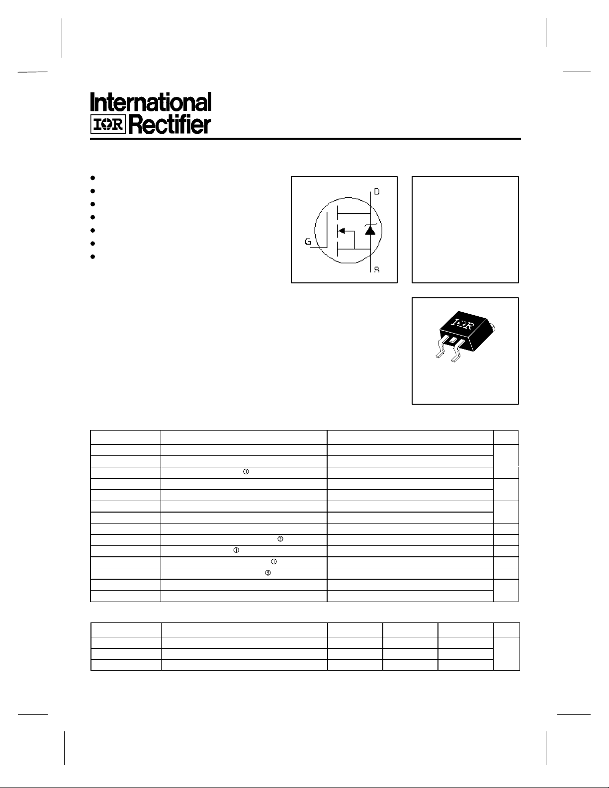
Continuous Source Current MOSFET symbol
(Body Diode) showing the
Pulsed Source Current integral reverse
(Body Diode) p-n junction diode.
––– ––– 41
A
––– ––– 160
Diode Forward Voltage ––– ––– 2.5 V TJ = 25°C, IS = 25A, VGS = 0V
Reverse Recovery Time ––– 140 210 ns TJ = 25°C, IF = 25A
Reverse RecoveryCharge ––– 0.79 1.2 µC di/dt = 100A/µs
Forward Turn-On Time
Intrinsic turn-on time is negligible (turn-on is dominated by LS+LD)
I
≤ 25A, di/dt ≤ 170A/µs, V
SD
DD
≤ V
(BR)DSS
,
TJ ≤ 175°C
Pulse width ≤ 300µs; duty cycle ≤ 2%.
= 25A. (See Figure 12)
AS
IRF1310S
GS
, Gate-to-Source Voltage (V)
D
I , Drain-to-So urce Current (A)
To Order
Next Data SheetIndex
Previous Datasheet
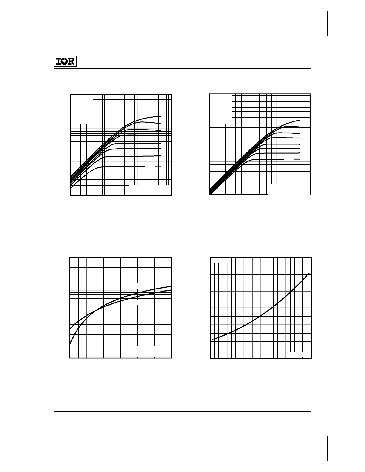
1000
VG S
TOP 15V
10V
8.0V
7.0V
6.0V
5.5V
5.0V
BOTTOM 4.5V
100
10
D
I , Drain-to-Source Current (A)
4.5V
20µs PULSE WIDTH
T = 25°C
1
0.1 1 1 0 100
V , D rain-to-Source Voltage (V)
DS
C
Fig 1. Typical Output Characteristics,
TC = 25oC
1000
1000
VGS
TOP 15V
10V
8.0V
7.0V
6.0V
5.5V
5.0V
BOTTOM 4.5V
100
10
D
I , Drain-to-Source Current (A)
4.5V
20µs PULSE WIDTH
T = 175°C
1
0.1 1 10 10 0
V , Drain-to-Source Voltage (V)
DS
C
Fig 2. Typical Output Characteristics,
TC = 175oC
3.0
I = 25A
D
100
10
1
4 5 6 7 8 9 10
Fig 3. Typical Transfer Characteristics Fig 4. Normalized On-Resistance
2.5
T = 25°C
J
T = 175°C
J
V = 50V
DS
20µ s PULS E WID TH
V
2.0
1.5
(Normalized)
1.0
0.5
DS(on)
R , Drain-to-Source On Resistance
0.0
-6 0 -40 -20 0 20 4 0 60 8 0 100 120 140 160 180
T , Junction Temperature (°C)
J
V = 10V
GS
Vs. Temperature

IRF1310S
To Order
Next Data SheetIndex
Previous Datasheet
400 0
300 0
200 0
C, Capacitance (pF)
100 0
0
1 10 10 0
V = 0V, f = 1MHz
GS
C = C + C , C SHORTED
iss gs gd ds
C = C
rss gd
C = C + C
oss ds gd
C
iss
C
oss
C
rss
V , Drain-to-Source Voltage (V)
DS
Fig 5. Typical Capacitance Vs.
Drain-to-Source Voltage
1000
20
I = 25A
D
16
12
8
4
GS
V , Gate-to-Source Voltage (V)
0
0 30 60 90 120
Q , Total Gate Charge (nC)
G
V = 80V
DS
V = 50V
DS
V = 20V
DS
FOR TEST CIRCUIT
SEE FIGURE 13
Fig 6. Typical Gate Charge Vs.
Gate-to-Source Voltage
1000
OPERATION IN THIS AREA LIMITED
BY R
DS(on)
100
10
SD
I , Reverse Drain Current (A)
1
0 0.5 1 1.5 2 2.5
Fig 7. Typical Source-Drain Diode
T = 175°C
J
T = 25°C
J
V = 0V
GS
V , Source-to-Drain Voltage (V)
SD
Forward Voltage
100
10
D
I , Drain Current (A)
T = 25°C
C
T = 175°C
J
Single Pulse
1
1 10 100 1000
V , D rain-to-Source Voltage (V)
DS
10µs
100µs
1ms
10ms
100ms
Fig 8. Maximum Safe Operating Area

50
t , Re ctangula r Pulse Duration (sec)
1
thJC
Thermal Re sponse (Z )
To Order
Next Data SheetIndex
Previous Datasheet
40
30
20
D
I , Drain Current (Amps)
10
0
25 50 7 5 100 125 150 175
T , Case Temperature (°C)
C
IRF1310S
R
V
DS
V
GS
R
G
10 V
Pulse Width ≤ 1 µs
Duty Factor ≤ 0.1 %
Fig 10a. Switching Time Test Circuit
D
D.U.T.
V
DD
Fig 9. Maximum Drain Current Vs.
Fig 10b. Switching Time Waveforms
Case Temperature
1
D = 0 .50
0.2 0
0.1 0
0.1
P
0.0 5
0.0 2
0.01
0.01
0.0 0 0 0 1 0.0001 0 .001 0.01 0.1 1 10
Fig 11. Maximum Effective Transient Thermal Impedance, Junction-to-Case
S ING LE PUL S E
(T H E R M AL R E S P O NSE)
Notes:
1. Duty fa ctor D = t / t
2. Peak T = P x Z + T
DM
J
DM
t
1
t
2
2
1
th JC
C

IRF1310S
To Order
Next Data SheetIndex
Previous Datasheet
10 V
Fig 12a. Unclamped Inductive Test Circuit
Fig 12b. Unclamped Inductive Waveforms
600
500
400
300
200
100
AS
V = 50V
E , Single Pulse Avalanche Energy (mJ)
DD
0
25 50 75 10 0 125 150 175
Starting T , Junction Temperature (°C)
J
I
TOP 10A
18A
BOTTOM 25A
Fig 12c. Maximum Avalanche Energy
Vs. Drain Current
D
10 V
Fig 13a. Basic Gate Charge Waveform Fig 13b. Gate Charge Test Circuit

Package Outline
To Order
Next Data SheetIndex
Previous Datasheet
SMD-220 Outline
IRF1310S

IRF1310S
To Order
Next Data SheetIndex
Previous Datasheet
Part Marking Information
Package Outline
SMD-220 Tape and Reel
IR CANADA: 7321 Victoria Park Ave., Suite 201, Markham, Ontario L3R 3L1, Tel: (905) 475 1897 IR GERMANY:
Saalburgstrasse 157, 61350 Bad Homburg Tel: 6172 37066 IR ITALY: Via Liguria 49, 10071 Borgaro, Torino Tel: (39) 1145
10111 IR FAR EAST: K&H Bldg., 2F, 3-30-4 Nishi-Ikeburo 3-Chome, Toshima-Ki, Tokyo 171 Tel: (03)3983 0641 IR
SOUTHEAST ASIA: 315 Outram Road, #10-02 Tan Boon Liat Building, 0316 Tel: 65 221 8371
WORLD HEADQUARTERS: 233 Kansas St., El Segundo, California 90245, Tel: (310) 322 3331
EUROPEAN HEADQUARTERS: Hurst Green, Oxted, Surrey RH8 9BB, UK Tel: (44) 0883 713215
Data and specifications subject to change without notice.
 Loading...