

Page 1
®
www.BDTIC.com/Intersil
ISL95310
Digitally Controlled Potentiometer (XDCP™)
Datasheet May 6, 2005 FN8083.0
Terminal Voltage 0V to 13.2V, 128 Taps
Up/Down Interface
The Intersil ISL95310 is a digitally controlled potentiometer
(XDCP). The device consists of a resistor array, wiper
switches, a control section, and nonvolatile memory. The
wiper position is controlled by an Up/Down interface.
The potentiometer is implemented by a resistor array
composed of 127 resistive elements and a wiper switching
network. Between each element and at either end are tap
points accessible to the wiper terminal. The wiper of each
potentiometer has an associated volatile Wiper Counter
Register (WR) and a non-volatile Initial Value Register (IVR)
that can be directly written to and read by the user. The
contents of the WR controls the position of the wiper on the
resistor array through the switches. At power-up, the device
recalls the contents of the default data registers to the
corresponding WR. The position of the wiper element is
controlled by the CS
, U/D, and INC inputs. The position of
the wiper can be stored in nonvolatile memory and then be
recalled upon a subsequent power-up operation.
The device can be used as a three-terminal potentiometer or
as a two-terminal variable resistor in a wide variety of
applications including:
• LCD contrast control
• Parameter and bias adjustments
• Mechanical potentiometer replacement
• Industrial and automotive control
Ordering Information
RESISTANCE
OPTION
PART NUMBER
ISL95310WIU10Z
(See Note)
ISL95310UIU10Z
(See Note)
Add “-TK” suffix for tape and reel.
(Ω)
10K -40 to +85 10 Ld MSOP
50K -40 to +85 10 Ld MSOP
TEMP
RANGE
(°C) PACKAGE
(Pb-Free)
(Pb-Free)
Features
• Non-volatile solid-state potentiometer
• Up/down interface with chip select enable
• DCP terminal voltage, 0 to +13.2V
• 128 wiper tap points - 0.8% resolution
- Wiper position stored in nonvolatile memory and
recalled on power-up
• 127 resistive elements
- Temperature compensated
- Low wiper resistance 70Ω typical @ 3.3V
• Low power CMOS
- Standby current, 2µA at V
= +3.6V
CC
• High reliability
- Endurance, 200,000 data changes per bit
- Register data retention 50 years @ T ≤ 75°C
•R
values = 10kΩ, 50kΩ
TOTAL
• 10-lead MSOP package
- Pb-free plus anneal available (RoHS compliant)
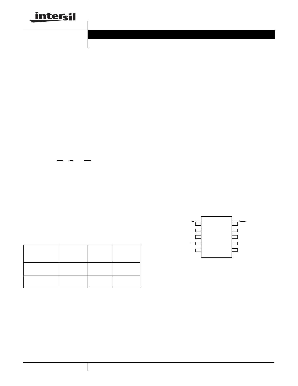
Pinout
ISL95310
(10 LD MSOP)
TOP VIEW
U/D
GND
V
CC
CS
NC
1
2
3
4
5
INC
10
9
V+
8
R
L
7
R
W
R
6
H
NOTE: Intersil Pb-free plus anneal products employ special Pbfree material sets; molding compounds/die attach materials and
100% matte tin plate termination finish, which are RoHS compliant
and compatible with both SnPb and Pb-free soldering operations.
Intersil Pb-free products are MSL classified at Pb-free peak reflow
temperatures that meet or exceed the Pb-free requirements of
IPC/JEDEC J STD-020.
1
CAUTION: These devices are sensitive to electrostatic discharge; follow proper IC Handling Procedures.
1-888-INTERSIL or 321-724-7143
XDCP is a trademark of Intersil Americas Inc. Copyright Intersil Americas Inc. 2005. All Rights Reserved
| Intersil (and design) is a registered trademark of Intersil Americas Inc.
All other trademarks mentioned are the property of their respective owners.
Page 2
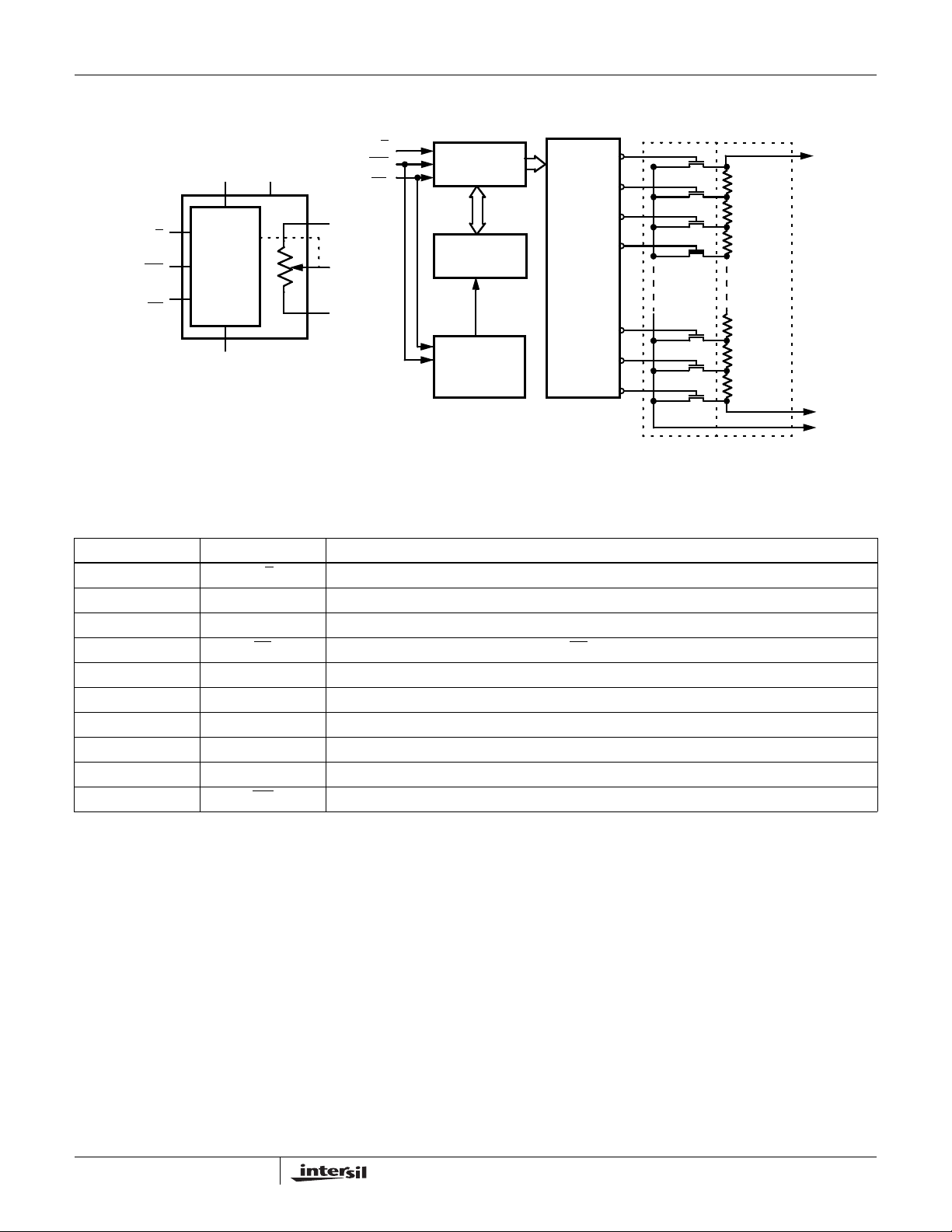
Block Diagram
www.BDTIC.com/Intersil
ISL95310
Up/Down
(U/D
Increment
(INC
Device Select
(CS
VCC
)
CONTROL
)
)
AND
MEMORY
GND
SIMPLE BLOCK DIAGRAM
V+
U/D
INC
CS
R
H
R
W
R
L
7-BIT
UP/DOWN
COUNTER
7-BIT
NONVOLATILE
MEMORY
STORE AND
RECALL
CONTROL
CIRCUITRY
ONE
OF
128
DECODER
DETAILED BLOCK DIAGRAM
Pin Descriptions
PIN NUMBER SYMBOL DESCRIPTION
1U/DControls the direction of wiper movement and whether the counter is incremented or decremented
2 GND Ground
3V
CC
4CSChip select; the device is selected when the CS input is LOW; also used to initiate a nonvolatile store
5 NC No connect; pin is to be left unconnected
6R
7R
8R
H
W
L
9 V+ Positive bias voltage for the potentiometer wiper control
10 INC
Positive logic supply voltage
A fixed terminal for one end of the potentiometer resistor
The wiper terminal which is equivalent to the movable terminal of a potentiometer
A fixed terminal for one end of the potentiometer resistor
Increment input; negative edge triggered
127
126
125
124
R
H
TRANSFER
GATES
2
1
0
RESISTOR
ARRAY
R
L
R
W
2
FN8083.0
May 6, 2005
Page 3
ISL95310
www.BDTIC.com/Intersil
Absolute Maximum Ratings Recommended Operating Conditions
Storage temperature . . . . . . . . . . . . . . . . . . . . . . . .-65°C to +150°C
Voltage on CS
with respect to GND. . . . . . . . . . . . . . . . . . . . -0.3V to V
Voltage on V+ (referenced to GND). . . . . . . . . . . . . . . . . . . . +13.2V
ΔV = |V
, RL, RW . . . . . . . . . . . . . . . . . . . . . . . . . . . . . . . . . . . . . . . . . .V+
R
H
Lead temperature (soldering 10s) . . . . . . . . . . . . . . . . . . . . .+300°C
(10s) . . . . . . . . . . . . . . . . . . . . . . . . . . . . . . . . . . . . . . . . . . ±6mA
I
W
. . . . . . . . . . . . . . . . . . . . . . . . . . . . . . . . . . . . . . . .-0.3V to +6V
V
CC
Power rating of each DCP . . . . . . . . . . . . . . . . . . . . . . . . . . . .20mW
CAUTION: Stresses above those listed under “Absolute Maximum Ratings” may cause permanent damage to the device. This is a stress rating only; functional
operation of the device (at these or any other conditions above those listed in the operational sections of this specification) is not implied. Exposure to absolute
maximum rating conditions for extended periods may affect device reliability.
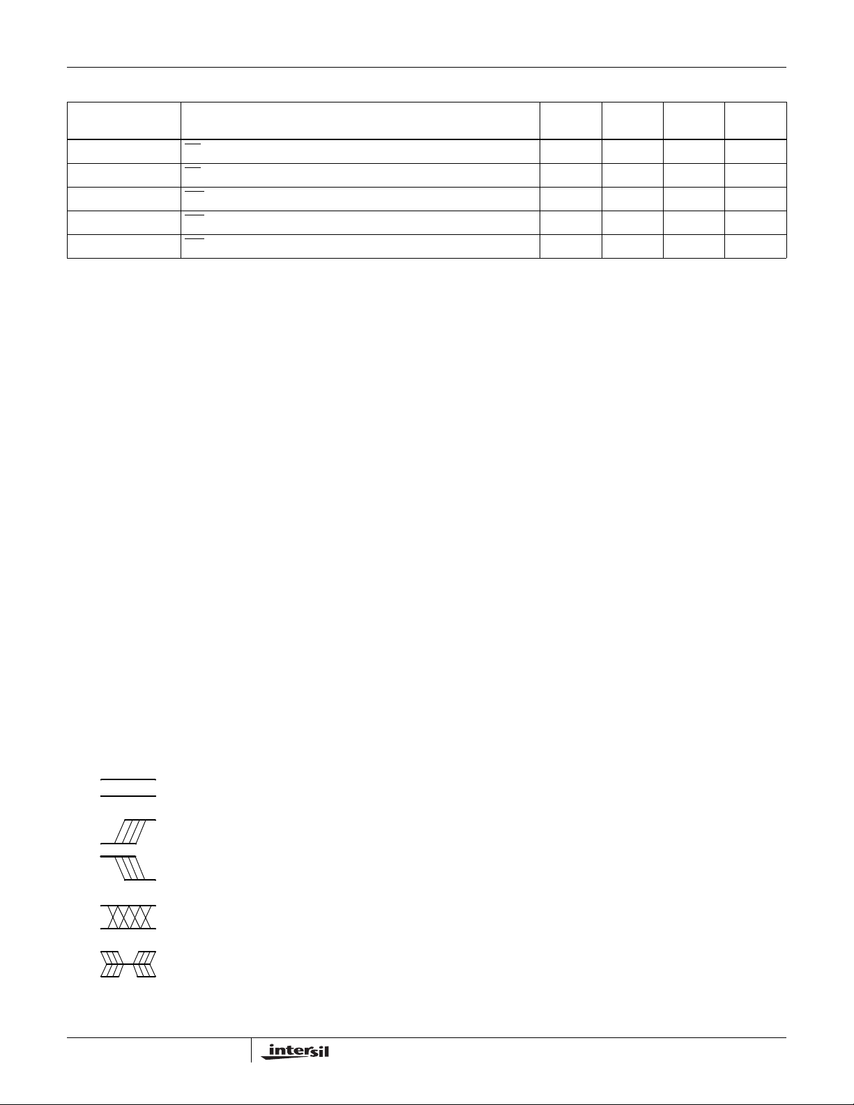
Analog Specifications Over recommended operating conditions unless otherwise stated.
SYMBOL PARAMETER TEST CONDITIONS MIN
R
TOTAL
V
R
C
H/CL/CW
I
LkgDCP
VOLTAGE DIVIDER MODE (0V @ R
INL
(Note 6)
(RH)-V(RL)
RH
W
, INC, U/D
+0.3V
CC
|. . . . . . . . . . . . . . . . . . . . . . . . . . . . . . . . . . . . .V+
RH to RL resistance W option 10 k Ω
U option 50 kΩ
R
to RL resistance tolerance -20 +20 %
H
RH terminal voltage VRL = 0V 0 V+ V
Wiper resistance V+ = 12V, wiper current = V+ / R
Potentiometer Capacitance (Note 13) 10/10/
Leakage on DCP pins Voltage at pin from GND to V+ 0.1 1 µA
; V+ @ RH; measured at RW, unloaded)
L
Integral non-linearity -1 1 LSB
Temperature Range (Industrial). . . . . . . . . . . . . . . . .-40°C to +85°C
. . . . . . . . . . . . . . . . . . . . . . . . . . . . . . . . . . . . . . . . 2.7V to 5.5V
V
CC
V+ . . . . . . . . . . . . . . . . . . . . . . . . . . . . . . . . . . . . . . . . 8.0V to 13.2V
Wiper current of each DCP . . . . . . . . . . . . . . . . . . . . . . . . . .±3.0mA
TYP
(Note 1) MAX UNIT
TOTAL
70 200 Ω
pF
25
(Note 2)
DNL
(Note 5)
ZSerror
(Note 3)
FSerror
(Note 4)
(Note 7) Ratiometric Temperature Coefficient DCP register set to 40 hex ±4 ppm/°C
TC
V
RESISTOR MODE (Measurements between R
RINL
(Note 11)
RDNL
(Note 10)
Roffset
(Note 9)
TC
(Note 12)
Differential non-linearity W option -0.75 0.75 LSB
U option -0.5 0.5
Zero-scale error U option 0 1 7 LSB
W option 0 0.5 2
Full-scale error U option -7 -1 0 LSB
W option -2 -1 0
and RL with RH not connected, or between RW and RH with RL not connected)
W
Integral non-linearity DCP register set between 20 hex and 7F hex;
monotonic over all tap positions
Differential non-linearity W option -0.75 0.75 MI
U option -0.5 0.5
Offset DCP Register set to 00 hex, W option 0 1 7 MI
DCP Register set to 00 hex, U option 0 0.5 2 MI
Resistance Temperature Coefficient DCP register set between 20 hex and 7F hex ±45 ppm/°C
R
-1 1 MI
(Note 2)
(Note 2)
(Note 2)
(Note 8)
(Note 8)
(Note 8)
(Note 8)
3
FN8083.0
May 6, 2005
Page 4
ISL95310
www.BDTIC.com/Intersil
Operating Specifications Over the recommended operating conditions unless otherwise specified.
SYMBOL PARAMETER TEST CONDITIONS MIN
I
CC1
I
CC2
I
SB
I
V+
I
LkgDig
I
LI
I
V+
t
DCP
(Note 13)
Vpor
(Note 13)
V
Ramp
CC
(Note 13)
t
D
(Note 13)
EEPROM SPECS
SERIAL INTERFACE SPECS
V
V
IH
Hysteresis
(Note 13)
Cpin
(Note 13)
VCC supply current, volatile write/read CS = VIL, U/D = VIL or VIH and INC = 0.4V/2.4V
min; t
VCC supply current, nonvolatile write CS = VIL, U/D = VIL or VIH and INC = 0.4V/2.4V
VCC current, standby V
V+ bias current V+ = 13.2V; V
Leakage current, at pins INC, CS,
, A0, and A1 pins
U/D
CS input leakage current VIN = V
V+ bias current V+ = 13.2V; V
DCP wiper response time INC
Power-on recall voltage Minimum V
VCC ramp rate 0.2 V/ms
Power up delay V
EEPROM endurance 150,000 Cycles
EEPROM retention Temperature ≤ 75°C 50 Years
INC, CS, and U/D -0.3 0.3*
IL
INC, CS, and U/D 0.7*
INC
, CS, and U/D input buffer
hysteresis
, CS, and U/D pin capacitance 10 pF
INC
min; t
CC
V
CC
Voltage at pin from GND to V
= 3V, CS = 0 60 100 150 µA
V
CC
= 5V, CS = 0 120 200 250 µA
V
CC
falling edge of last bit of DCP data byte to
wiper change
above Vpor, to DCP initial value register
CC
recall completed, and 2-wire Interface in standby
state
, RH, RW not connected
CYC RL
, RH, RW not connected
CYC RL
= +5.5V, 2-wire interface in standby state 5 µA
= +3.6V, 2-wire interface in standby state 2 µA
= +5.5V 1 µA
CC
CC
CC
= +5.5V 1 µA
CC
at which memory recall occurs 1.8 2.6 V
CC
TYP
(Note 1) MAX UNIT
1mA
3mA
-10 10 µA
±1 µA
1µs
3ms
V
CC
VCC+
V
CC
0.05*
V
CC
0.3
V
V
V
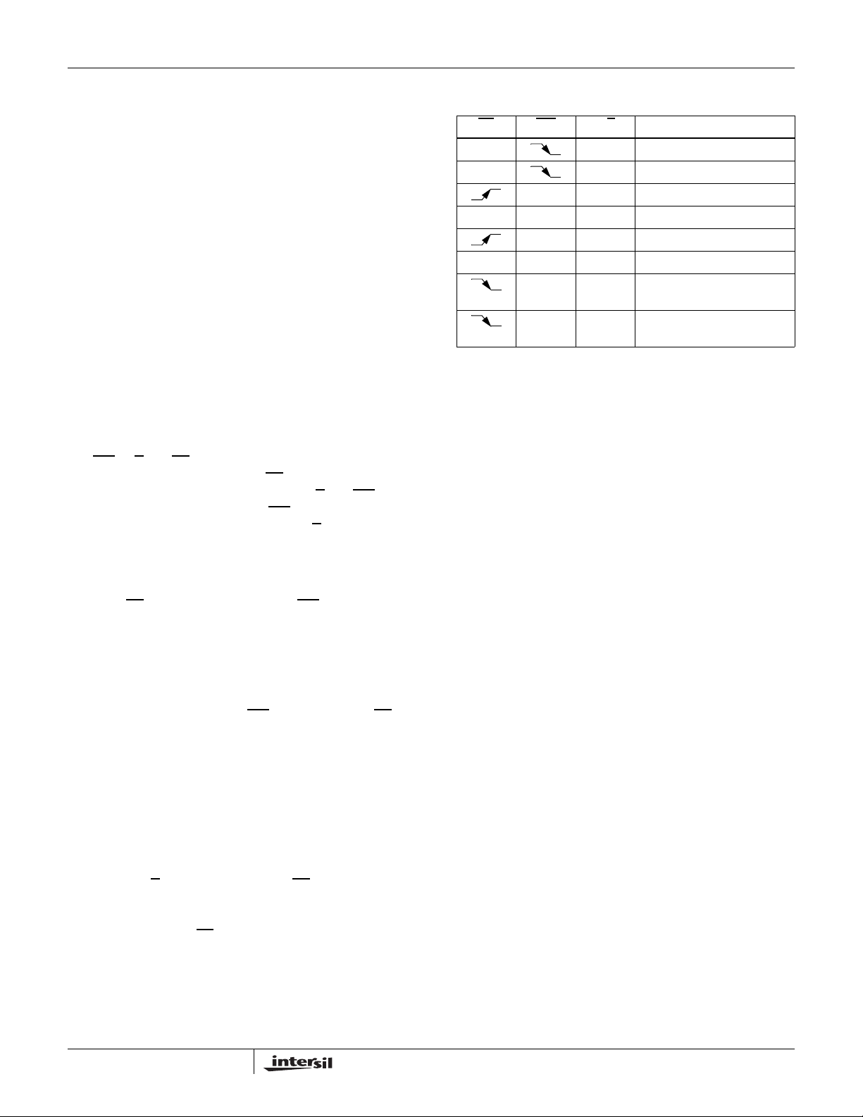
AC Electrical Specifications V
SYMBOL PARAMETER MIN
t
Cl
(Note 13) INC HIGH to U/D change 100 ns
t
lD
t
(Note 13) U/D to INC setup 1 µs
DI
t
lL
t
lH
t
lC
CS to INC setup 100 ns
INC LOW period 1 µs
INC HIGH period 1 µs
INC inactive to CS inactive 1 µs
= 5V ±10%, TA = Full Operating Temperature Range unless otherwise stated
CC
4
TYP
(Note 4) MAX UNIT
FN8083.0
May 6, 2005
Page 5
ISL95310
www.BDTIC.com/Intersil
AC Electrical Specifications V
SYMBOL PARAMETER MIN
t
CPHS
(Note 13) CS deselect time (NO STORE) 1 µs
t
CPHNS
t
(Note 13) INC to RW change 100 500 µs
IW
t
CYC
(Note 13) INC input rise and fall time 500 µs
t
R, tF
NOTES:
1. Typical values are for T
2. LSB: [V(R
incremental voltage when changing from one tap to an adjacent tap.
3. ZS error = V(R
4. FS error = [V(R
5. DNL = [V(R
6. INL = V(R
TC
7.
for i = 16 to 120 decimal, T = -40°C to 85°C. Max( ) is the maximum value of the wiper voltage and Min ( ) is the minimum value of the wiper
voltage over the temperature range.
8. MI =
9. Roffset = R
Roffset = R
10. RDNL = (R
11. RINL = [R
12.
TC
for i = 16 to 127, T = -40°C to 85°C. Max( ) is the maximum value of the resistance and Min ( ) is the minimum value of the resistance over the
temperature range.
13. This parameter is not 100% tested.
14. t
WC
valid STOP condition at the end of a Write sequence of a 3-wire serial interface Write operation, to the end of the self-timed internal non-volatile
write cycle.
W)127
W)i
-------------------------------------------------------------------------------------------------x
V
Max V RW()
|R
– R
127
i
– (MI • i) – R0]/MI, for i = 16 to 127.
i
------------------------------------------------------------------
R
Max Ri()Min Ri()+[]2§
is the minimum cycle time to be allowed for any non-volatile Write by the user, unless Acknowledge Polling is used. It is the time from a
CS deselect time (STORE) 20 ms
INC cycle time 4 µs
= 25°C and 3.3V supply voltage.
A
– V(RW)0]/127. V(RW)
/LSB.
W)0
– V+]/LSB.
W)127
– V(RW)
W)i
– (i • LSB – V(RW)0) for i = 1 to 127.
Max V RW()
()Min V RW()
()Min V RW()
| /127. R
0
/MI, when measuring between RW and RL.
0
/MI, when measuring between RW and RH.
127
– R
i-1
Max Ri()Min Ri()–[]
]/LSB-1, for i = 1 to 127. i is the DCP register setting.
i-1
i
()+[]2§
i
and R0 are the measured resistances for the DCP register set to 7F hex and 00 hex respectively.
127
)/MI, for i = 16 to 127.
= 5V ±10%, TA = Full Operating Temperature Range unless otherwise stated (Continued)
CC
TYP
(Note 4) MAX UNIT
and V(RW)0 are V(RW) for the DCP register set to 7F hex and 00 hex respectively . LSB is the
127
()–
---------------- -
×=
125°C
10
i
i
6
6
10
---------------- -=
125°C
Symbol Table
WAVEFORM INPUTS OUTPUTS
Must be steady Will be steady
May change from Low to High Will change from Low to High
May change from High to Low
Don’t Care: Changes Allowed Changing: State Not Known
N/A
Will change from High to Low
Center Line is High Impedance
5
FN8083.0
May 6, 2005
Page 6

A.C. Timing
www.BDTIC.com/Intersil
CS
t
CI
INC
ISL95310
t
CYC
t
IL
t
IH
t
IC
t
CPHS
90% 90%
10%
t
CPHNS
U/D
R
t
ID
t
IW
W
t
DI
(3)
MI
Power Up and Down Requirements
In order to prevent unwanted tap position changes, or an
inadvertent store, bring the CS
concurrently with the V
CC
and INC high before or
pin on power-up. The
potentiometer voltages must be applied after this sequence
is completed. During power-up, the data sheet parameters
for the DCP do not fully apply until 1ms after V
final value. The V
ramp spec is always in effect.
CC
reaches its
CC
Pin Descriptions
RH and R
The high (R
equivalent to the fixed terminals of a mechanical
potentiometer. The terminology of R
relative position of the terminal in relation to wiper movement
direction selected by the U/D
potential on the terminal.
L
) and low (RL) terminals of the ISL95310 are
H
and RH references the
L
input and not the voltage
t
F
CS
is returned HIGH while the INC input is also HIGH. After
t
R
the store operation is complete the ISL95310 will be placed
in the low power standby mode until the device is selected
once again.
Principles of Operation
There are three sections of the ISL95310: the input control,
counter and decode section; the nonvolatile memory; and
the resistor array. The input control section operates just like
an up/down counter. The output of this counter is decoded to
turn on a single electronic switch connecting a point on the
resistor array to the wiper output. Under the proper
conditions the contents of the counter can be stored in
nonvolatile memory and retained for future use. The resistor
array is comprised of 127 individual resistors connected in
series. At either end of the array and between each resistor
is an electronic switch that transfers the potential at that
point to the wiper.
R
W
RW is the wiper terminal and is equivalent to the movable
terminal of a mechanical potentiometer. The position of the
wiper within the array is determined by the control inputs.
Up/Down (U/D)
The U/D input controls the direction of the wiper movement
and whether the counter is decremented.
Increment (INC)
The INC input is negative-edge triggered. Toggling INC will
move the wiper and either increment or decrement the
counter in the direction indicated by the logic level on the
U/D
input.
Chip Select (CS)
The wiper, when at either fixed terminal, acts like its
mechanical equivalent and does not move beyond the last
position. That is, the counter does not wrap around when
clocked to either extreme.
The electronic switches on the device operate in a “make
before break” mode when the wiper changes tap positions. If
the wiper is moved several positions, multiple taps are
connected to the wiper for t
R
value for the device can temporarily be reduced by
TOTAL
a significant amount if the wiper is moved several positions.
When the device is powered-down, the last wiper position
stored will be maintained in the nonvolatile memory. When
power is restored, the contents of the memory are recalled
and the wiper is set to the value last stored.
The device is selected when the CS input is LOW. The
current counter value is stored in nonvolatile memory when
6
(INC to VW change). The
IW
FN8083.0
May 6, 2005
Page 7
On applying power to the ISL95310, the VCC supply should
www.BDTIC.com/Intersil
have a monotonic ramp to the specified operating voltage. It
is important that once V
least 2.5V in less than 7.5ms (0.2V/ms). The ramp rate
before and after these thresholds is not important.
V
must be applied prior to, or simultaneously, with V+.
CC
Under no condition should V+ be applied without V
the sequence of applying V+ and V
not affect the proper recall of the wiper position, applying V+
before V
before the electronic switch control signals are applied. This
can result in multiple electronic switches being turned on,
which could load the power supply and cause brief,
unexpected potentiometer wiper settings.
To prevent unknown wiper positions on the ISL95310 on
power down, it is recommended that V+ turn off before or
simultaneously with V
off, the wiper position can remain unchanged from its
previous setting or it can go to an undefined state.
powers the electronic switches of the DCP
CC
reaches 1V that it increases to at
CC
to the ISL95310 does
CC
. If V+ remains on after VCC turns
CC
CC
. While
Instructions and Programming
The INC, U/D and CS inputs control the movement of the
wiper along the resistor array. With CS
is selected and enabled to respond to the U/D
inputs. HIGH to LOW transitions on INC
decrement (depending on the state of the U/D
bit counter. The output of this counter is decoded to select
one of one hundred wiper positions along the resistive array.
set LOW the device
and INC
will increment or
input) a seven
ISL95310
TABLE 1. MODE SELECTION
CS
L H Wiper up
L L Wiper down
H X X Standby current
H H X Standby
INC U/D MODE
H X Store wiper position
L X No store, return to standby
L H Wiper up one position
(not recommended)
L L Wiper down one position
(not recommended)
The value of the counter is stored in nonvolatile memory
whenever CS
HIGH.
The system may select the ISL95310, move the wiper and
deselect the device without having to store the latest wiper
position in nonvolatile memory. After the wiper movement is
performed as described above and once the new position is
reached, the system must keep INC
HIGH. The new wiper position will be maintained until
changed by the system or until a power-up/down cycle
recalled the previously stored data.
This procedure allows the system to always power-up to a
preset value stored in nonvolatile memory; then during
system operation minor adjustments could be made. The
adjustments might be based on user preference, system
parameter changes due to temperature drift, etc.
The state of U/D
This allows the host system to enable the device and then
move the wiper up and down until the proper trim is attained.
During initial power-up CS
V
to avoid an accidental store generation.
CC
transitions HIGH while the INC input is also
LOW while taking CS
may be changed while CS remains LOW.
must go high along with or before
7
FN8083.0
May 6, 2005
Page 8
Packaging Information
www.BDTIC.com/Intersil
ISL95310
10 Lead MSOP, Package Code
0.0433 [1.10] MAX.
0.0106 [0.27]
0.0067 [0.17]
10
9876
1
2
45
3
0.0197 [0.50] BSC
0.1220 [3.10]
0.1142 [2.90]
0.0039 [0.10] MAX. (S)
2
4
0.1970 [5.00]
0.1890 [4.80]
0.0374 [0.95]
0.0295 [0.75]
0.0059 [0.15]
0.0020 [0.05]
(S)
(S)
WITH PLATING
0.0098 [0.25]
GAUGE PLANE
0.0276 [0.70]
0.0157 [0.40]
0.0091 [0.23]
0.0051 [0.13]
0.0106 [0.27]
0.0067 [0.17]
WITH
PLATING
0.0080 [0.203]
REF
SECTION A-A
0.1220 [3.10]
0.1142 [2.90]
0.1220 [3.10]
0.1142 [2.90]
4
0.0050 [0.127]
BASE
METAL
3
3
A
0°-6°
A
NOTES:
1. Package dimensions conform to JEDEC specification MO-187BA.
2
2. Does not include mold flash, protrusion
or gate burrs, mold flash protrusions
or gate burrs shall not exceed 0.15 mm per side.
3
3. Does not include interlead flash or protrusion. Interlead flash or protrusion shall not exceed 0.15 mm per side.
4
4. Does not include dambar protrusion. Allowable dambar protrusion shall be 0.8 mm.
5. Lead span/stand-off height/coplanarity are considered as special characteristics.
6. Controlling dimensions in inches [mm].
All Intersil U.S. products are manufactured, assembled and tested utilizing ISO9000 quality systems.
Intersil Corporation’s quality certifications can be viewed at www.intersil.com/design/quality
Intersil products are sold by description only. Intersil Corporation reserves the right to make changes in circuit design, software and/or specifications at any time without
notice. Accordingly, the reader is cautioned to verify that data sheets are current before placing orders. Information furnished by Intersil is believed to be accurate and
reliable. However, no responsibility is assumed by Intersil or its subsidiaries for its use; nor for any infringements of patents or other rights of third parties which may result
from its use. No license is granted by implic atio n or other wise u nde r any p a tent or patent rights of Intersil or its subsidi ari es.
For information regarding Intersil Corporation and its products, see www.intersil.com
8
FN8083.0
May 6, 2005
 Loading...