

Page 1
3+1 Voltage Regulator for IMVP-7/VR12™ CPUs
ISL95831
Compliant with IMVP-7/VR12™, the ISL95831 provides a
complete solution for microprocessor and graphic processor
core power supply. It provides two Voltage Regulators (VRs)
with three integrated gate drivers. The first VR can be
configured as 3-, 2- or 1-phase VR while the second output is 1phase VR, providing maximum flexibility. The two VRs share the
serial control bus to communicate with the CPU and achieve
lower cost and smaller board area compared with the two-chip
approach.
Based on Intersil’s Robust Ripple Regulator (R3) technology™,
the PWM modulator compared to traditional modulators, has
faster transient settling time, variable switching frequency
during load transients and has improved light load efficiency
with it’s ability to automatically change switching frequency.
The ISL95831 has several other key features. Both outputs
support DCR current sensing with single NTC thermistor for
DCR temperature compensation or accurate resistor current
sensing. Both outputs come with remote voltage sense,
programmable V
voltage, programmable I
BOOT
MAX
, T
MAX
,
adjustable switching frequency, OC protection and separate
Power-Good.
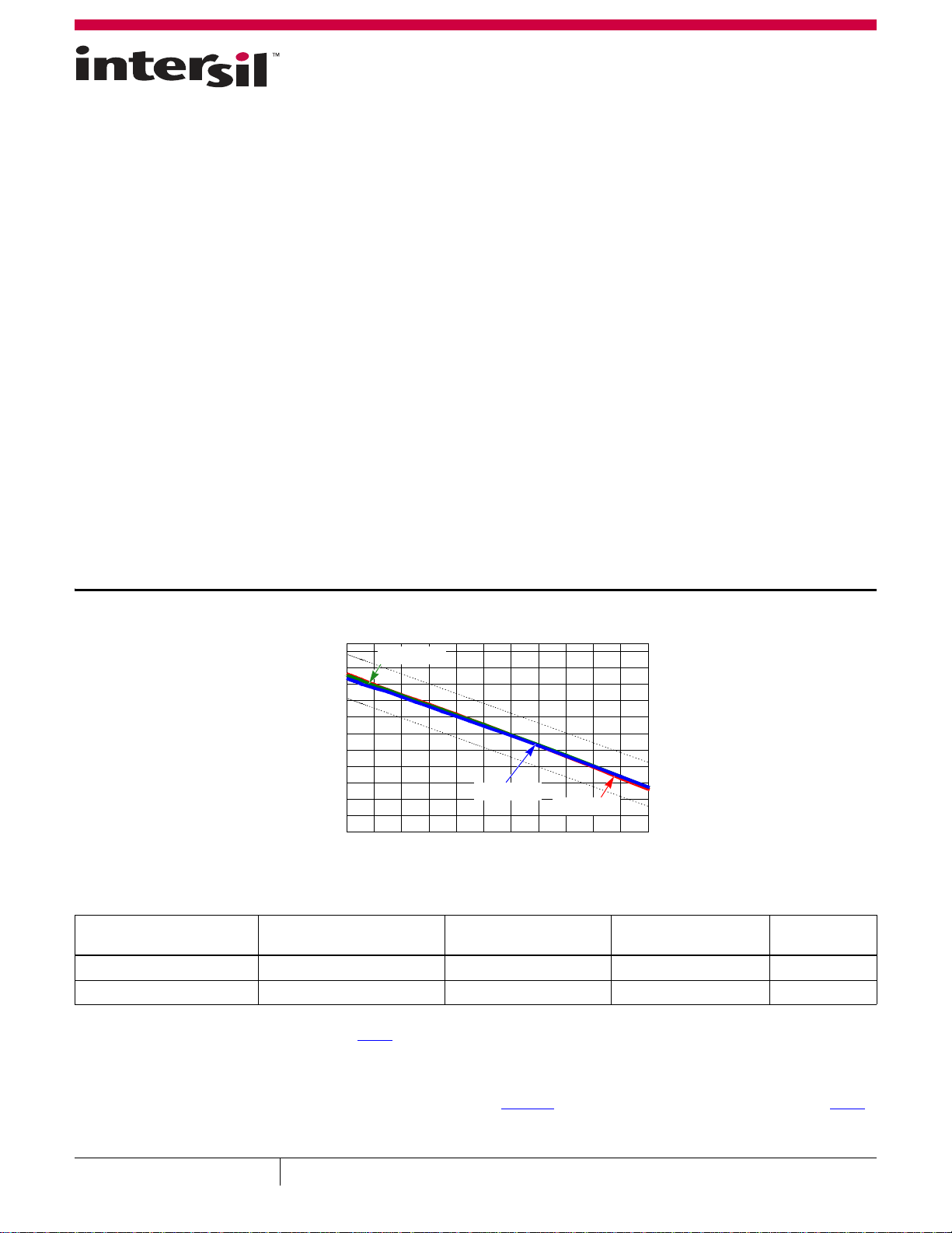
Load Line Regulation
0.91
0.90
0.89
0.88
0.87
0.86
(V)
0.85
OUT
V
0.84
0.83
0.82
0.81
0.80
VIN = 19V
0 6 12 18 24
Features
•Serial Data Bus
•Dual Outputs:
- Configurable 3-, 2- or 1-phase for the 1st Output using 2
integrated Gate Drivers
- 1-phase for the 2nd Output using an Integrated Gate
Driver
• 0.5% System Accuracy Over-Temperature
• Supports Multiple Current Sensing Methods
- Lossless Inductor DCR Current Sensing
- Precision Resistor Current Sensing
• Differential Remote Voltage Sensing
•Programmable V
• Resistor Programmable I
Voltage at Start-up
BOOT
MAX
, T
for Both Outputs
MAX
• Adaptive Body Diode Conduction Time Reduction
Applications
• IMVP-7/VR12 Compliant Computers
VIN = 12V
VIN = 8V
30 36 42 48 54 60 66
(A)
I
OUT
Ordering Information
PART NUMBER
(Notes 1, 2, 3) PART MARKING
ISL95831HRTZ 95831 HRTZ -10 to +100 48 Ld 6x6 TQFN L48.6x6
ISL95831IRTZ 95831 IRTZ -40 to +100 48 Ld 6x6 TQFN L48.6x6
NOTES:
1. Add “-T*” suffix for tape and reel. Please refer to TB347
2. These Intersil Pb-free plastic packaged products employ special Pb-free material sets, molding compounds/die attach materials, and 100% matte
tin plate plus anneal (e3 termination finish, which is RoHS compliant and compatible with both SnPb and Pb-free soldering operations). Intersil Pbfree products are MSL classified at Pb-free peak reflow temperatures that meet or exceed the Pb-free requirements of IPC/JEDEC J STD-020.
3. For Moisture Sensitivity Level (MSL), please see device information page for ISL95831
January 21, 2011
FN7613.0
1
for details on reel specifications.
CAUTION: These devices are sensitive to electrostatic discharge; follow proper IC Handling Procedures.
1-888-INTERSIL or 1-888-468-3774
TEMP. RANGE
(°C)
. For more information on MSL please see techbrief TB363.
Intersil (and design) is a trademark owned by Intersil Corporation or one of its subsidiaries.
All other trademarks mentioned are the property of their respective owners.
|Copyright Intersil Americas Inc. 2011. All Rights Reserved
PACKAGE
(Pb-Free)
PKG.
DWG. #
Page 2
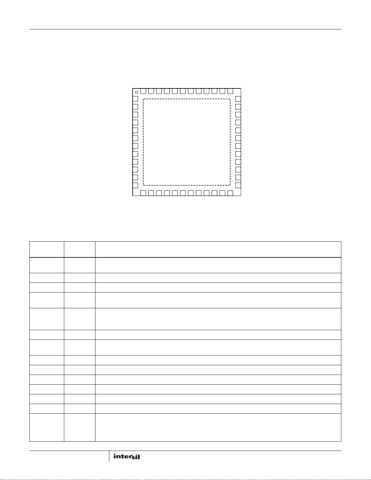
Pin Configuration
VWG
IMONG
PGOODG
SDA
ALERT#
SCLK
VR_ON
PGOOD
IMON
VR_HOT#
NTC
VW
ISL95831
ISL95831
(48 LD TQFN)
TOP VIEW
RTNG
ISUMPG
GND PAD
(BOTTOM)
ISEN2
ISEN1
ISUMNG
VSEN
NTCG
RTN
FBG
COMPG
48 47 46 45 44 43 42 41 40 39
1
2
3
4
5
6
7
8
9
10
11
12
13 14 15 16 17 18 19 20 21 22
VSENG
FB
COMP
ISEN3/FB2
PROG2
BOOTG
UGATEGVDD
PHASEG
LGATEG
38 37
36
BOOT2
35
UGATE2
PHASE2
34
VSSP2
33
32
LGATE2
VCCP
31
30
PWM3
29
LGATE1
VSSP1
28
PHASE1
27
UGATE1
26
25
BOOT1
23 24
VIN
ISUMP
ISUMN
PROG1
Pin Descriptions
ISL95831
PIN NUMBER SYMBOL DESCRIPTION
BOTTOM PAD GND Signal common of the IC. Unless otherwise stated, signals are referenced to the GND pin. It should also be used as the
thermal pad for heat removal.
1 VWG A resistor from this pin to COMPG programs the switching frequency for VR2 (8kΩ gives approximately 300kHz).
2 IMONG An analog output. IMONG outputs a current proportional to VR2 output current.
3 PGOODG Power-Good open-drain output indicating when VR2 is able to supply regulated voltage. Pull up externally with a 680Ω
4, 5, 6 SDA,
ALERT#,
SCLK
7 VR_ON Controller enable input. A high level logic signal on this pin enables the controller.
8 PGOOD Power-Good open-drain output indicating when VR1 is able to supply regulated voltage. Pull up externally with a 680Ω
9 IMON An analog output. IMON outputs a current proportional to VR1 output current.
10 VR_HOT# Open drain thermal overload output indicator. Can be considered part of communication bus with CPU.
11 NTC One of the thermistor inputs to VR_HOT# circuit. Use it to monitor VR1 temperature.
12 VW A resistor from this pin to COMP programs the switching frequency for VR1 (8kΩ gives approximately 300kHz).
13 COMP This pin is the output of the error amplifier for VR1.
14 FB This pin is the inverting input of the error amplifier for VR1.
15 ISEN3/FB2 When the VR1 is configured in 3-phase mode, this pin is ISEN3. ISEN3 is the individual current sensing for VR1 phase 3.
resistor to VCCP or 1.9kΩ to 3.3V.
Communication bus between the CPU and the VRs.
resistor to VCCP or 1.9kΩ to 3.3V.
When VR1 is configured in 2-phase mode, this pin is FB2. There is a switch between the FB2 pin and the FB pin. The
switch is on when VR1 is in 2-phase mode and is off in 1-phase mode. The components connecting to FB2 are used to
adjust the compensation in 1-phase mode to achieve optimum performance for VR1.
2
FN7613.0
January 21, 2011
Page 3

ISL95831
Pin Descriptions (Continued)
ISL95831
PIN NUMBER SYMBOL DESCRIPTION
16 ISEN2 Individual current sensing for VR1 Phase 2. When ISEN2 and PWM3 are both pulled to 5V VDD, the controller will
disable VR1 Phases 3 and 2.
17 ISEN1 Individual current sensing for VR1 Phase 1.
18 VSEN VR1 remote voltage sense input.
19 RTN VR1 remote voltage sense return.
20, 21 ISUMN and
ISUMP
22 VDD 5V bias power.
23 VIN This pin is connected to the power stage input voltage and used for feed-forward.
24 PROG1 A resistor from this pin to GND programs Imax for VR1, and V
25 BOOT1 Connect an MLCC capacitor across the BOOT1 and the PHASE1 pins. The boot capacitor is charged through an internal
26 UGATE1 Output of VR1 Phase-1 high-side MOSFET gate driver. Connect the UGATE1 pin to the gate of the Phase-1 high-side
27 PHASE1 Current return path for the VR1 Phase-1 high-side MOSFET gate driver. Connect the PHASE1 pin to the node consisting
28 VSSP1 Current return path for VR1 Phase-1 low-side MOSFET gate driver. Connect the VSSP1 pin to the source of VR1 Phase-
29 LGATE1 Output of VR1 Phase-1 low-side MOSFET gate driver. Connect the LGATE1 pin to the gate of VR1 Phase-1 low-side
30 PWM3 PWM output for VR1 Phase 3. When PWM3 is pulled to 5V VDD, the controller will disable VR1 Phase 3.
31 VCCP Input voltage bias for the internal gate drivers. Connect +5V to the VCCP pin. Decouple with at least 1µF of an MLCC
32 LGATE2 Output of VR1 Phase-2 low-side MOSFET gate driver. Connect the LGATE2 pin to the gate of VR1 Phase-2 low-side
33 VSSP2 Current return path for VR1 Phase-2 low-side MOSFET gate driver. Connect the VSSP2 pin to the source of VR1 Phase-2
34 PHASE2 Current return path for VR1 Phase-2 high-side MOSFET gate driver. Connect the PHASE2 pin to the node consisting of
35 UGATE2 Output of VR1 Phase-2 high-side MOSFET gate driver. Connect the UGATE2 pin to the gate of VR1 Phase-2 high-side
36 BOOT2 Connect an MLCC capacitor across the BOOT2 and the PHASE2 pins. The boot capacitor is charged through an internal
37 LGATEG Output of VR2 low-side MOSFET gate driver. Connect the LGATEG pin to the gate of VR2 low-side MOSFET.
38 PHASEG Current return path for VR2 high-side MOSFET gate driver. Connect the PHASEG pin to the node consisting of the
39 UGATEG Output of VR2 high-side MOSFET gate driver. Connect the UGATEG pin to the gate of VR2 high-side MOSFET.
40 BOOTG Connect an MLCC capacitor across the BOOTG and the PHASEG pins. The boot capacitor is charged through an internal
41 PROG2 A resistor from this pin to GND programs I
42 NTCG The second thermistor input to VR_HOT# circuit. Use it to monitor VR2 temperature.
VR1 droop current sense input.
for both VR1 and VR2.
BOOT
boot diode connected from the VCCP pin to the BOOT1 pin, each time the PHASE1 pin drops below VCCP minus the
voltage dropped across the internal boot diode.
MOSFET.
of the high-side MOSFET source, the low-side MOSFET drain, and the output inductor of VR1 Phase 1.
1 low-side MOSFET through a low impedance path, preferably in parallel with the traces connecting the LGATE1 pin to
the gates of the Phase-1 low-side MOSFET.
MOSFET.
capacitor.
MOSFET.
low-side MOSFET through a low impedance path, preferably in parallel with the traces connecting the LGATE2 pin to
the gates of the Phase-2 low-side MOSFET.
the high-side MOSFET source, the low-side MOSFET drain, and the output inductor of VR1 Phase 2.
MOSFET.
boot diode connected from the VCCP pin to the BOOT2 pin, each time the PHASE2 pin drops below VCCP minus the
voltage dropped across the internal boot diode.
high-side MOSFET source, the low-side MOSFET drain, and the output inductor of VR2.
boot diode connected from the VCCP pin to the BOOTG pin, each time the PHASEG pin drops below VCCP minus the
voltage dropped across the internal boot diode.
for VR2 and T
MAX
for both VR1 and VR2.
MAX
3
FN7613.0
January 21, 2011
Page 4
ISL95831
Pin Descriptions (Continued)
ISL95831
PIN NUMBER SYMBOL DESCRIPTION
43, 44 ISUMNG and
ISUMPG
45 RTNG VR2 remote voltage sense return.
46 VSENG VR2 remote voltage sense input.
47 FBG This pin is the inverting input of the error amplifier for VR2.
48 COMPG This pin is the output of the error amplifier for VR2. Also, a resistor from COMPG to GND can program the operational
VR2 droop current sense input. When ISUMNG is pulled to 5V VDD, VR2 is disabled and all communication to VR2 is
rejected.
modes of VR2.
4
FN7613.0
January 21, 2011
Page 5
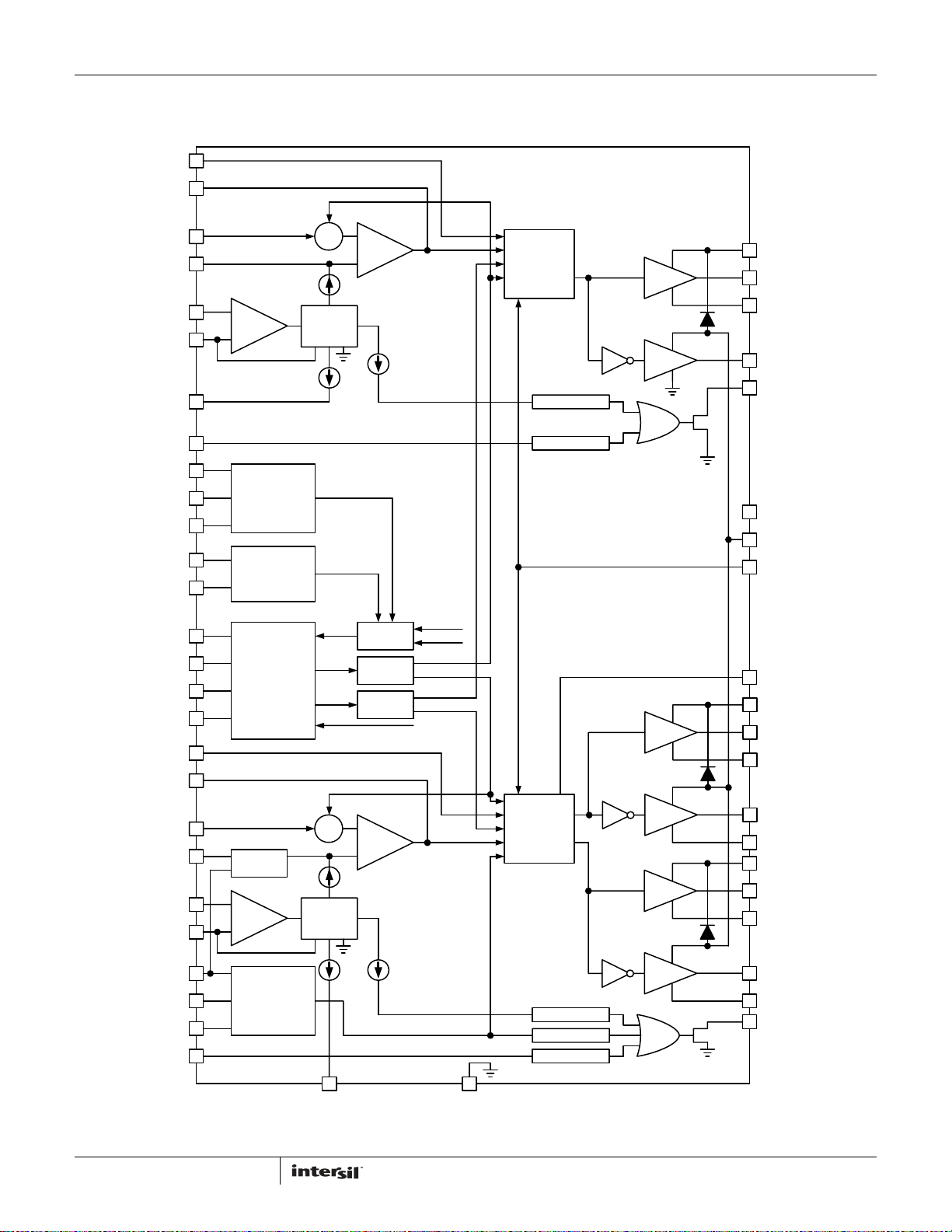
Block Diagram
VWG
COMPG
RTNG
FBG
ISUMPG
ISUMNG
ISL95831
+
+
+
_
CURRENT
SENSE
Σ
+
E/A
_
IDROOPG
VR2
MODULATOR
DRIVER
DRIVER
BOOTG
UGATEG
PHASEG
LGATEG
IMONG
VSENG
NTCG
NTC
VR_HOT#
PROG2
PROG1
VR_ON
SDA
ALERT#
SCLK
VW
COMP
RTN
FB
ISUMP
ISUMN
TEMP
MONITOR
IMAX
VBOOT
TMAX
SET (A/D)
DIGITAL
INTERFACE
FB2
CIRCUIT
+
_
T_MONITOR
PROG
+
+
Σ
CURRENT
SENSE
MODE
+
E/A
_
IDROOP
IMONG
A/D IMON
DAC2
DAC1
D/A
MODE2
MODE1
VREADY
OC FAULT
OV FAULT
VR1
MODULATOR
DRIVER
DRIVER
DRIVER
PGOODG
VDD
VCCP
VIN
PWM3
BOOT2
UGATE2
PHASE2
LGATE2
VSSP2
BOOT1
UGATE1
PHASE1
ISEN3/FB2
ISEN2
ISEN1
VSEN
CURRENT
BALANCING
5
DRIVER
OC FAULT
IBAL FAULT
OV FAULT
GNDIMON
LGATE1
VSSP1
PGOOD
January 21, 2011
FN7613.0
Page 6
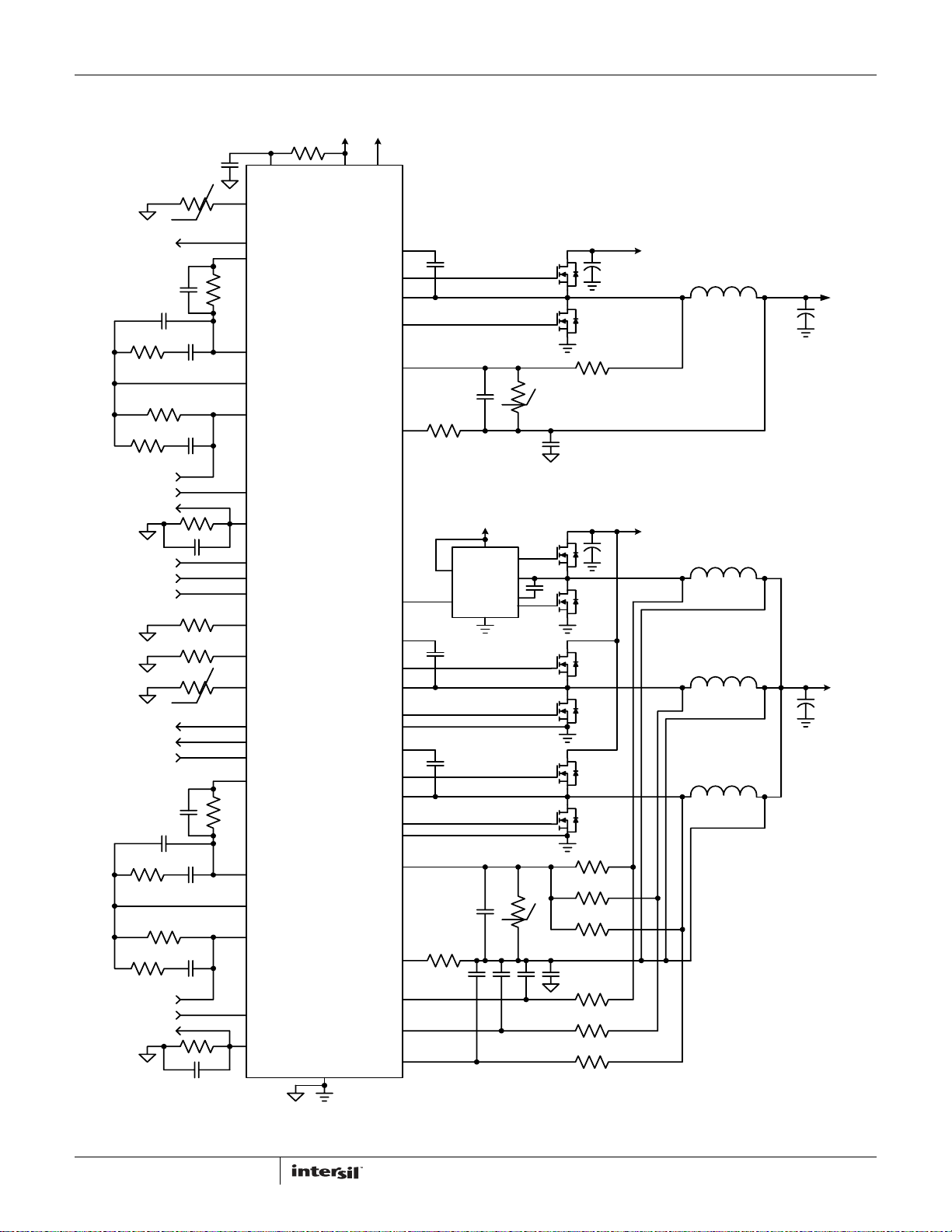
Simplified Application Circuit
V+5
ISL95831
VIN
Rntcg
°c
PGOODG PGOODG
Rdroopg
VCCSENSEG
VSSSENSEG
IMONG
SDA SDA
ALERT# ALERT#
SCLK SCLK
Rprog2
Rprog1
Rntc
°c
VR_HOT# VR_HOT#
PGOOD
VR_ON
Rdroop
VCCSENSE
VSSSENSE
IMON
NTCG
VWG
Rfsetg
COMPG
FBG
VSENG
RTNG
IMONG
PROG2
PROG1
NTC
PGOOD
VR_ON
VW
Rfset
COMP
FB
VSEN
RTN
IMON
VDD
ISL95831
GND
PVCC
VIN
BOOTG
UGATEG
PHASEG
LGATEG
ISUMPG
ISUMNG
PWM3
BOOT2
UGATE2
PHASE2
LGATE2
VSSP2
BOOT1
UGATE1
PHASE1
LGATE1
VSSP1
ISUMP
ISUMN
ISEN3/FB2
ISEN2
ISEN1
Rig
Ri
Cng
FCCM
ISL6208
PWM
Cn
V+5
VCC
GND
°c
UGATE
PHASE
BOOT
LGATE
°c
Cisen3Cisen2Cisen1
Rng
Vsumng
Rn
Cvsumng
Vsumn
Cvsumv
Rsum4
Rsum3
Rsum2
Rsum1
Risen3
Risen2
Risen1
Vin
Vin
L4
L3
L2
L1
AXG Vcore
CPU Vcore
FIGURE 1. TYPICAL ISL95831 APPLICATION CIRCUIT USING INDUCTOR DCR SENSING
6
FN7613.0
January 21, 2011
Page 7
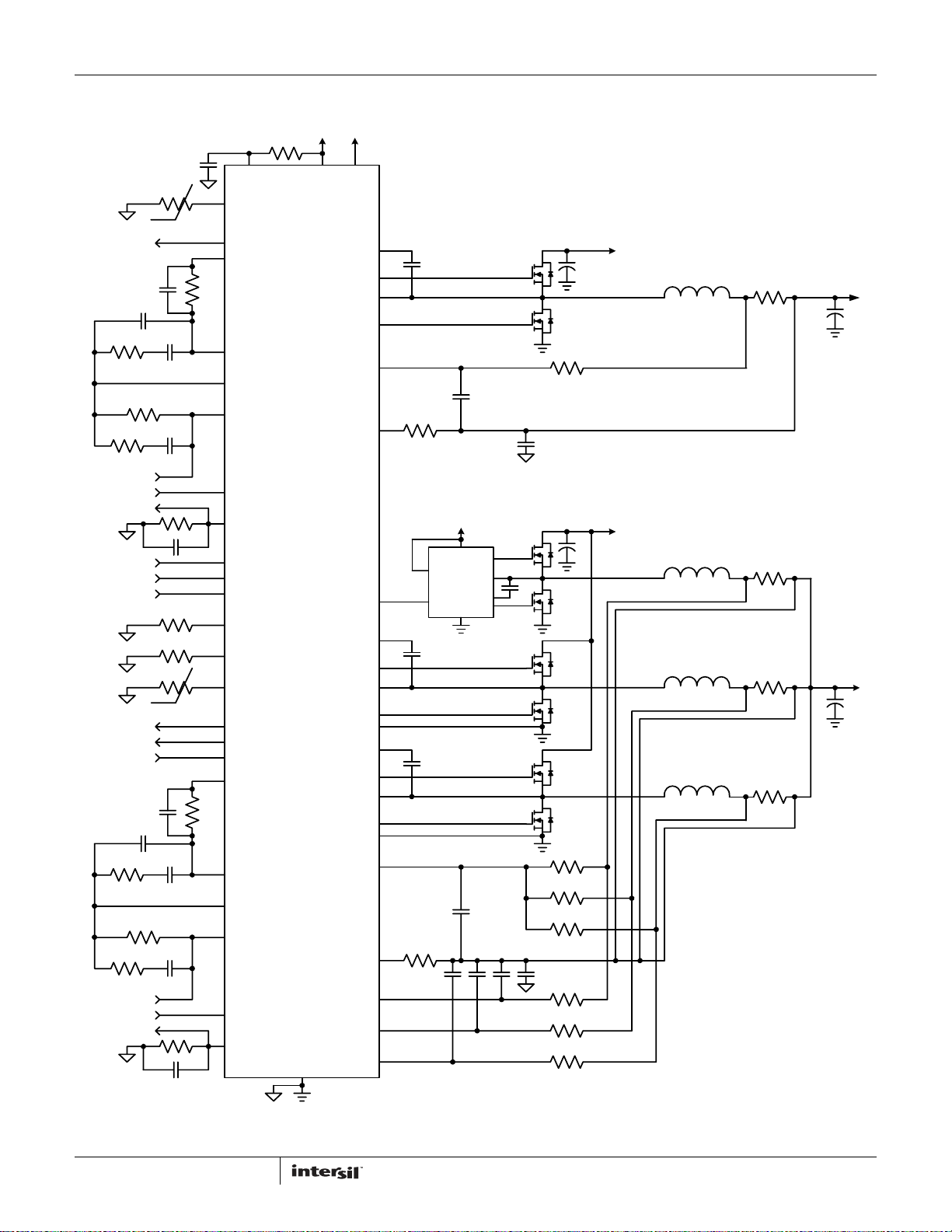
Simplified Application Circuit
V+5
VIN
PVCC
VDD
Rntcg
°C
NTCG
VIN
ISL95831
PGOODG PGOODG
Rfsetg
Rdroopg
VCCSENSEG
VSSSENSEG
IMONG
SDA SDA
ALERT# ALERT#
SCLK SCLK
Rprog2
Rprog1
Rntc
°C
VR_HOT# VR_HOT#
PGOOD
VR_ON
Rfset
Rdroop
VCCSENSE
VSSSENSE
IMON
VWG
COMPG
FBG
VSENG
RTNG
IMONG
PROG2
PROG1
NTC
PGOOD
VR_ON
VW
COMP
FB
VSEN
RTN
IMON
ISL95831
GND
BOOTG
UGATEG
PHASEG
LGATEG
ISUMPG
ISUMNG
PWM3
BOOT2
UGATE2
PHASE2
LGATE2
VSSP2
BOOT1
UGATE1
PHASE1
LGATE1
VSSP1
ISUMP
ISUMN
ISEN3/FB2
ISEN2
ISEN1
Vin
L4
Rsum4
Cng
Rig
V+5
VCC
FCCM
ISL6208
PWM
GND
Cn
Ri
UGATE
PHASE
BOOT
LGATE
Cisen3Cisen2Cisen1
Vsumng
Cvsumng
Vin
L3
L2
L1
Rsum3
Rsum2
Rsum1
Vsumn
Cvsumn
Risen3
Risen2
Risen1
Rsen4
Rsen3
Rsen2
Rsen1
AXG Vcore
CPU Vcore
FIGURE 2. TYPICAL ISL95831 APPLICATION CIRCUIT USING RESISTOR SENSING
7
FN7613.0
January 21, 2011
Page 8

ISL95831
Table of Contents
Load Line Regulation . . . . . . . . . . . . . . . . . . . . . . . . . . . . . . . . . . . . . . . . . . . . . . . . . . . . . . . . . . . . . . . . . . . . . . . . . . . . . . . . . . . . 1
Pin Descriptions. . . . . . . . . . . . . . . . . . . . . . . . . . . . . . . . . . . . . . . . . . . . . . . . . . . . . . . . . . . . . . . . . . . . . . . . . . . . . . . . . . . . . . . . . 2
Block Diagram . . . . . . . . . . . . . . . . . . . . . . . . . . . . . . . . . . . . . . . . . . . . . . . . . . . . . . . . . . . . . . . . . . . . . . . . . . . . . . . . . . . . . . . . . . 5
Simplified Application Circuit . . . . . . . . . . . . . . . . . . . . . . . . . . . . . . . . . . . . . . . . . . . . . . . . . . . . . . . . . . . . . . . . . . . . . . . . . . . 6
Simplified Application Circuit . . . . . . . . . . . . . . . . . . . . . . . . . . . . . . . . . . . . . . . . . . . . . . . . . . . . . . . . . . . . . . . . . . . . . . . . . . . 7
Absolute Maximum Ratings . . . . . . . . . . . . . . . . . . . . . . . . . . . . . . . . . . . . . . . . . . . . . . . . . . . . . . . . . . . . . . . . . . . . . . . . . . . . . . . 9
Thermal Information . . . . . . . . . . . . . . . . . . . . . . . . . . . . . . . . . . . . . . . . . . . . . . . . . . . . . . . . . . . . . . . . . . . . . . . . . . . . . . . . . . . . . 9
Recommended Operating Conditions. . . . . . . . . . . . . . . . . . . . . . . . . . . . . . . . . . . . . . . . . . . . . . . . . . . . . . . . . . . . . . . . . . . . . . . 9
Gate Driver Timing Diagram. . . . . . . . . . . . . . . . . . . . . . . . . . . . . . . . . . . . . . . . . . . . . . . . . . . . . . . . . . . . . . . . . . . . . . . . . . . . . . 12
Theory of Operation . . . . . . . . . . . . . . . . . . . . . . . . . . . . . . . . . . . . . . . . . . . . . . . . . . . . . . . . . . . . . . . . . . . . . . . . . . . . . . . . . . . . 12
Multiphase R3™ Modulator. . . . . . . . . . . . . . . . . . . . . . . . . . . . . . . . . . . . . . . . . . . . . . . . . . . . . . . . . . . . . . . . . . . . . . . . . . . . 12
Diode Emulation and Period Stretching . . . . . . . . . . . . . . . . . . . . . . . . . . . . . . . . . . . . . . . . . . . . . . . . . . . . . . . . . . . . . . . . . 13
Start-up Timing . . . . . . . . . . . . . . . . . . . . . . . . . . . . . . . . . . . . . . . . . . . . . . . . . . . . . . . . . . . . . . . . . . . . . . . . . . . . . . . . . . . . . . 14
Voltage Regulation and Load Line Implementation . . . . . . . . . . . . . . . . . . . . . . . . . . . . . . . . . . . . . . . . . . . . . . . . . . . . . . . 14
Differential Voltage Sensing . . . . . . . . . . . . . . . . . . . . . . . . . . . . . . . . . . . . . . . . . . . . . . . . . . . . . . . . . . . . . . . . . . . . . . . . . . . 18
Phase Current Balancing . . . . . . . . . . . . . . . . . . . . . . . . . . . . . . . . . . . . . . . . . . . . . . . . . . . . . . . . . . . . . . . . . . . . . . . . . . . . . . 18
CCM Switching Frequency . . . . . . . . . . . . . . . . . . . . . . . . . . . . . . . . . . . . . . . . . . . . . . . . . . . . . . . . . . . . . . . . . . . . . . . . . . . . . 20
Modes of Operation . . . . . . . . . . . . . . . . . . . . . . . . . . . . . . . . . . . . . . . . . . . . . . . . . . . . . . . . . . . . . . . . . . . . . . . . . . . . . . . . . . .20
Dynamic Operation. . . . . . . . . . . . . . . . . . . . . . . . . . . . . . . . . . . . . . . . . . . . . . . . . . . . . . . . . . . . . . . . . . . . . . . . . . . . . . . . . . . 21
VR_HOT#/ALERT# Behavior . . . . . . . . . . . . . . . . . . . . . . . . . . . . . . . . . . . . . . . . . . . . . . . . . . . . . . . . . . . . . . . . . . . . . . . . . . . 21
Current Monitor. . . . . . . . . . . . . . . . . . . . . . . . . . . . . . . . . . . . . . . . . . . . . . . . . . . . . . . . . . . . . . . . . . . . . . . . . . . . . . . . . . . . . . 22
FB2 Function . . . . . . . . . . . . . . . . . . . . . . . . . . . . . . . . . . . . . . . . . . . . . . . . . . . . . . . . . . . . . . . . . . . . . . . . . . . . . . . . . . . . . . . . 22
Adaptive Body Diode Conduction Time Reduction . . . . . . . . . . . . . . . . . . . . . . . . . . . . . . . . . . . . . . . . . . . . . . . . . . . . . . . . .22
Protections . . . . . . . . . . . . . . . . . . . . . . . . . . . . . . . . . . . . . . . . . . . . . . . . . . . . . . . . . . . . . . . . . . . . . . . . . . . . . . . . . . . . . . . . . .23
Supported Data And Configuration Registers. . . . . . . . . . . . . . . . . . . . . . . . . . . . . . . . . . . . . . . . . . . . . . . . . . . . . . . . . . . . . 23
Key Component Selection . . . . . . . . . . . . . . . . . . . . . . . . . . . . . . . . . . . . . . . . . . . . . . . . . . . . . . . . . . . . . . . . . . . . . . . . . . . . . . . 24
Inductor DCR Current-Sensing Network . . . . . . . . . . . . . . . . . . . . . . . . . . . . . . . . . . . . . . . . . . . . . . . . . . . . . . . . . . . . . . . . . 24
Resistor Current-Sensing Network . . . . . . . . . . . . . . . . . . . . . . . . . . . . . . . . . . . . . . . . . . . . . . . . . . . . . . . . . . . . . . . . . . . . . 26
Overcurrent Protection . . . . . . . . . . . . . . . . . . . . . . . . . . . . . . . . . . . . . . . . . . . . . . . . . . . . . . . . . . . . . . . . . . . . . . . . . . . . . . . .26
Compensator. . . . . . . . . . . . . . . . . . . . . . . . . . . . . . . . . . . . . . . . . . . . . . . . . . . . . . . . . . . . . . . . . . . . . . . . . . . . . . . . . . . . . . . . 27
Programming Resistors . . . . . . . . . . . . . . . . . . . . . . . . . . . . . . . . . . . . . . . . . . . . . . . . . . . . . . . . . . . . . . . . . . . . . . . . . . . . . . .30
Current Monitor . . . . . . . . . . . . . . . . . . . . . . . . . . . . . . . . . . . . . . . . . . . . . . . . . . . . . . . . . . . . . . . . . . . . . . . . . . . . . . . . . . . . . .30
Current Balancing . . . . . . . . . . . . . . . . . . . . . . . . . . . . . . . . . . . . . . . . . . . . . . . . . . . . . . . . . . . . . . . . . . . . . . . . . . . . . . . . . . . .30
Slew Rate Compensation Circuit For VID Transition . . . . . . . . . . . . . . . . . . . . . . . . . . . . . . . . . . . . . . . . . . . . . . . . . . . . . . . .31
Layout Guidelines . . . . . . . . . . . . . . . . . . . . . . . . . . . . . . . . . . . . . . . . . . . . . . . . . . . . . . . . . . . . . . . . . . . . . . . . . . . . . . . . . . . . . . 35
Typical Performance . . . . . . . . . . . . . . . . . . . . . . . . . . . . . . . . . . . . . . . . . . . . . . . . . . . . . . . . . . . . . . . . . . . . . . . . . . . . . . . . . . . . 37
Revision History . . . . . . . . . . . . . . . . . . . . . . . . . . . . . . . . . . . . . . . . . . . . . . . . . . . . . . . . . . . . . . . . . . . . . . . . . . . . . . . . . . . . . . . 41
Products . . . . . . . . . . . . . . . . . . . . . . . . . . . . . . . . . . . . . . . . . . . . . . . . . . . . . . . . . . . . . . . . . . . . . . . . . . . . . . . . . . . . . . . . . . . . . . 41
Package Outline Drawing . . . . . . . . . . . . . . . . . . . . . . . . . . . . . . . . . . . . . . . . . . . . . . . . . . . . . . . . . . . . . . . . . . . . . . . . . . . . . . . 42
8
FN7613.0
January 21, 2011
Page 9
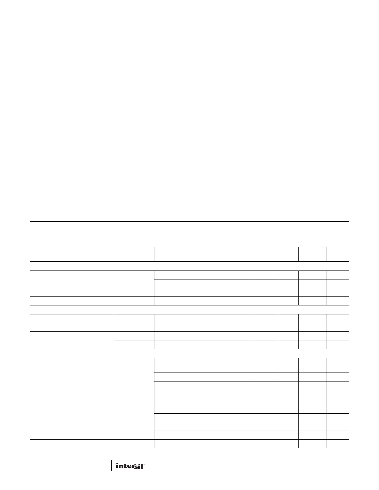
ISL95831
Absolute Maximum Ratings Thermal Information
Supply Voltage, VDD. . . . . . . . . . . . . . . . . . . . . . . . . . . . . . . . . . . -0.3V to +7V
Battery Voltage, VIN . . . . . . . . . . . . . . . . . . . . . . . . . . . . . . . . . . . . . . . . . +28V
Boot Voltage (BOOT). . . . . . . . . . . . . . . . . . . . . . . . . . . . . . . . . . -0.3V to +33V
Boot-to-Phase Voltage
(BOOT-PHASE) -0.3V to +7V(DC) . . . . . . . . . . . . . . -0.3V to +9V(<10ns)
Phase Voltage (PHASE) . . . . . . . . . . . . . . . . -7V (<20ns Pulse Width, 10µJ)
UGATE Voltage (UGATE) . . . . . . . . . . . . . . . . . . . PHASE - 0.3V (DC) to BOOT
. . . . . . . . . . . . . . . . . . . . PHASE - 5V (<20ns Pulse Width, 10µJ) to BOOT
LGATE Voltage
. . . . . . . . . . . . . . . . . . . . . . . . -2.5V (<20ns Pulse Width, 5µJ) to VDD+0.3V
All Other Pins . . . . . . . . . . . . . . . . . . . . . . . . . . . . . . . . . -0.3V to (VDD +0.3V)
Open Drain Outputs, PGOOD, VR_HOT#, ALERT#. . . . . . . . . . -0.3V to +7V
ESD Rating
Human Body Model (Tested per JESD22-A114E). . . . . . . . . . . . . . . . 2kV
Machine Model (Tested per JESD22-A115-A) . . . . . . . . . . . . . . . . . 200V
Charged Device Model (Tested per JESD22-C101A) . . . . . . . . . . . . . . 1k
Latch Up (Tested per JESD-78B; Class 2, Level A) . . . . . . . . . . . . . . 100mA
CAUTION: Do not operate at or near the maximum ratings listed for extended periods of time. Exposure to such conditions may adversely impact product
reliability and result in failures not covered by warranty.
NOTES:
4. θ
is measured in free air with the component mounted on a high effective thermal conductivity test board with “direct attach” features. See Tech
JA
Brief TB379.
5. For θ
, the “case temp” location is the center of the exposed metal pad on the package underside.
JC
Thermal Resistance (Typical) θ
48 Ld TQFN Package (Notes 4, 5) . . . . . . . 29 1
Maximum Junction Temperature . . . . . . . . . . . . . . . . . . . . . . . . . . . .+150°C
Maximum Storage Temperature Range . . . . . . . . . . . . . .-65°C to +150°C
Maximum Junction Temperature (Plastic Package) . . . . . . . . . . . .+150°C
Storage Temperature Range. . . . . . . . . . . . . . . . . . . . . . . .-65°C to +150°C
Pb-Free Reflow Profile . . . . . . . . . . . . . . . . . . . . . . . . . . . . . . . see link below
http://www.intersil.com/pbfree/Pb-FreeReflow.asp
(°C/W) θJC (°C/W)
JA
Recommended Operating Conditions
Supply Voltage, VDD. . . . . . . . . . . . . . . . . . . . . . . . . . . . . . . . . . . . . . +5V ±5%
Battery Voltage, VIN . . . . . . . . . . . . . . . . . . . . . . . . . . . . . . . . . . +4.5V to 25V
Ambient Temperature
HRTZ. . . . . . . . . . . . . . . . . . . . . . . . . . . . . . . . . . . . . . . . . . -10°C to +100°C
IRTZ . . . . . . . . . . . . . . . . . . . . . . . . . . . . . . . . . . . . . . . . . .-40°C to +100°C
Junction Temperature
HRTZ. . . . . . . . . . . . . . . . . . . . . . . . . . . . . . . . . . . . . . . . . .-10°C to +125°C
IRTZ . . . . . . . . . . . . . . . . . . . . . . . . . . . . . . . . . . . . . . . . . .-40°C to +125°C
Electrical Specifications "Operating Conditions: VDD = 5V, T
(ISL95831HRTZ), fSW = 300kHz, unless otherwise noted." Boldface limits apply over the operating temperature ranges, -10°C to +100°C or
= -40°C to +100°C (ISL95831IRTZ), TA = -10°C to +100°C
A
-40°C to +100°C.
PARAMETER SYMBOL TEST CONDITIONS
MIN
(Note 6) TYP
MAX
(Note 6) UNITS
INPUT POWER SUPPLY
+5V Supply Current I
Battery Supply Current I
Input Resistance R
V
IN
VDD
VIN
VIN
VR_ON = 1V 9.2 10.5 mA
VR_ON = 0V 1 µA
VR_ON = 0V 1 µA
VR_ON = 1V 550 kΩ
POWER-ON-RESET THRESHOLDS
VDD Power-On-Reset Threshold VDDPOR
VDDPOR
VIN Power-On-Reset Threshold VINPOR
VINPOR
VDD rising 4.35 4.5 V
r
VDD falling 4.00 4.15 V
f
VIN rising 4.00 4.35 V
r
VIN falling 2.8 3.3 V
f
SYSTEM AND REFERENCES
System Accuracy HRTZ
%Error (V
IRTZ
%Error (V
Internal V
Maximum Output Voltage V
BOOT
OUT(max)
No load; closed loop, active mode range,
VID = 0.75V to 1.52V, -0.5 +0.5 %
OUT)
VID = 0.5V to 0.745V -8 +8 mV
VID = 0.25V to 0.495V -15 +15 mV
No load; closed loop, active mode range,
)
VID = 0.75V to 1.52V -0.8 +0.8 %
OUT
VID = 0.5V to 0.745V -10 +10 mV
VID = 0.25V to 0.495V -18 +18 mV
HRTZ 1.0945 1.100 1.1055 V
IRTZ 1.0912 1.100 1.1088 V
VID = [11111111] 1.52 V
9
FN7613.0
January 21, 2011
Page 10
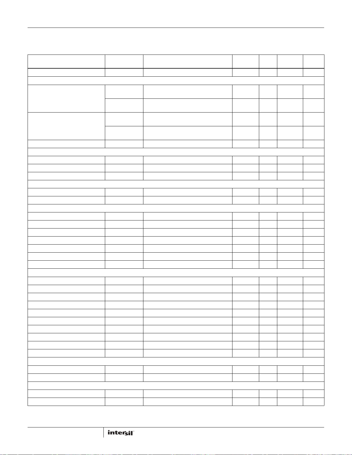
ISL95831
Electrical Specifications "Operating Conditions: VDD = 5V, T
(ISL95831HRTZ), fSW = 300kHz, unless otherwise noted." Boldface limits apply over the operating temperature ranges, -10°C to +100°C or
= -40°C to +100°C (ISL95831IRTZ), TA = -10°C to +100°C
A
-40°C to +100°C. (Continued)
PARAMETER SYMBOL TEST CONDITIONS
Minimum Output Voltage V
OUT(min)
MIN
(Note 6) TYP
VID = [00000001] 0.25 V
MAX
(Note 6) UNITS
CHANNEL FREQUENCY
Nominal Channel Frequency-HRTZ HRTZ_VR1
fSW(nom)
HRTZ_VR2
fSW(nom)
Nominal Channel Frequency-IRTZ IRTZ_VR1
fSW(nom)
IRTZ_VR2
fSW(nom)
R
= 8.66kΩ, 2-channel operation,
fset
V
= 1.1V
COMP
= 9.09kΩ, V
R
fset
R
= 8.66kΩ, 2-channel operation,
fset
V
= 1.1V
COMP
= 9.09kΩ, V
R
fset
= 1.1V 285 300 315 kHz
COMP
= 1.1V 280 300 320 kHz
COMP
285 300 315 kHz
280 300 320 kHz
Adjustment Range 200 500 kHz
AMPLIFIERS
Current-Sense Amplifier Input Offset I
Error Amp DC Gain A
v0
Error Amp Gain-Bandwidth Product GBW C
= 0A -0.15 +0.15 mV
FB
90 dB
= 20pF 18 MHz
L
ISEN
Imbalance Voltage Maximum of ISENs - Minimum of ISENs 1 mV
Input Bias Current 20 nA
POWER-GOOD AND PROTECTION MONITORS
I
PGOOD Low Voltage V
PGOOD Leakage Current I
OL
OH
= 4mA 0.15 0.4 V
PGOOD
PGOOD = 3.3V 1 µA
PGOOD Delay tpgd 1.2 ms
ALERT# Low Voltage 7 12 Ω
VR_HOT# Low Voltage 7 12 Ω
ALERT# Leakage Current 1 µA
VR_HOT# Leakage Current 1 µA
GATE DRIVER
UGATE Pull-Up Resistance R
UGATE Source Current I
UGATE Sink Resistance R
UGATE Sink Current I
LGATE Pull-Up Resistance R
LGATE Source Current I
LGATE Sink Resistance R
LGATE Sink Current I
UGATE to LGATE De adt ime t
LGATE to UGATE De adt ime t
UGPU
UGSRC
UGPD
UGSNK
LGPU
LGSRC
LGPD
LGSNK
UGFLGR
LGFUGR
200mA Source Current 1.0 1.5 Ω
UGATE - PHASE = 2.5V 2.0 A
250mA Sink Current 1.0 1.5 Ω
UGATE - PHASE = 2.5V 2.0 A
250mA Source Current 1.0 1.5 Ω
LGATE - VSSP = 2.5V 2.0 A
250mA Sink Current 0.5 0.9 Ω
LGATE - VSSP = 2.5V 4.0 A
UGATE falling to LGATE rising, no load 23 ns
LGATE falling to UGATE rising, no load 28 ns
BOOTSTRAP DIODE
Forward Voltage V
Reverse Leakage I
F
R
PVCC = 5V, IF = 2mA 0.58 V
VR = 25V 0.2 µA
PROTECTION
Overvoltage Threshold OV
H
VSEN rising above setpoint for >1µs 120 155 200 mV
Current Imbalance Threshold One ISEN above another ISEN for >1.2ms 9 mV
10
FN7613.0
January 21, 2011
Page 11
ISL95831
Electrical Specifications "Operating Conditions: VDD = 5V, T
(ISL95831HRTZ), fSW = 300kHz, unless otherwise noted." Boldface limits apply over the operating temperature ranges, -10°C to +100°C or
= -40°C to +100°C (ISL95831IRTZ), TA = -10°C to +100°C
A
-40°C to +100°C. (Continued)
PARAMETER SYMBOL TEST CONDITIONS
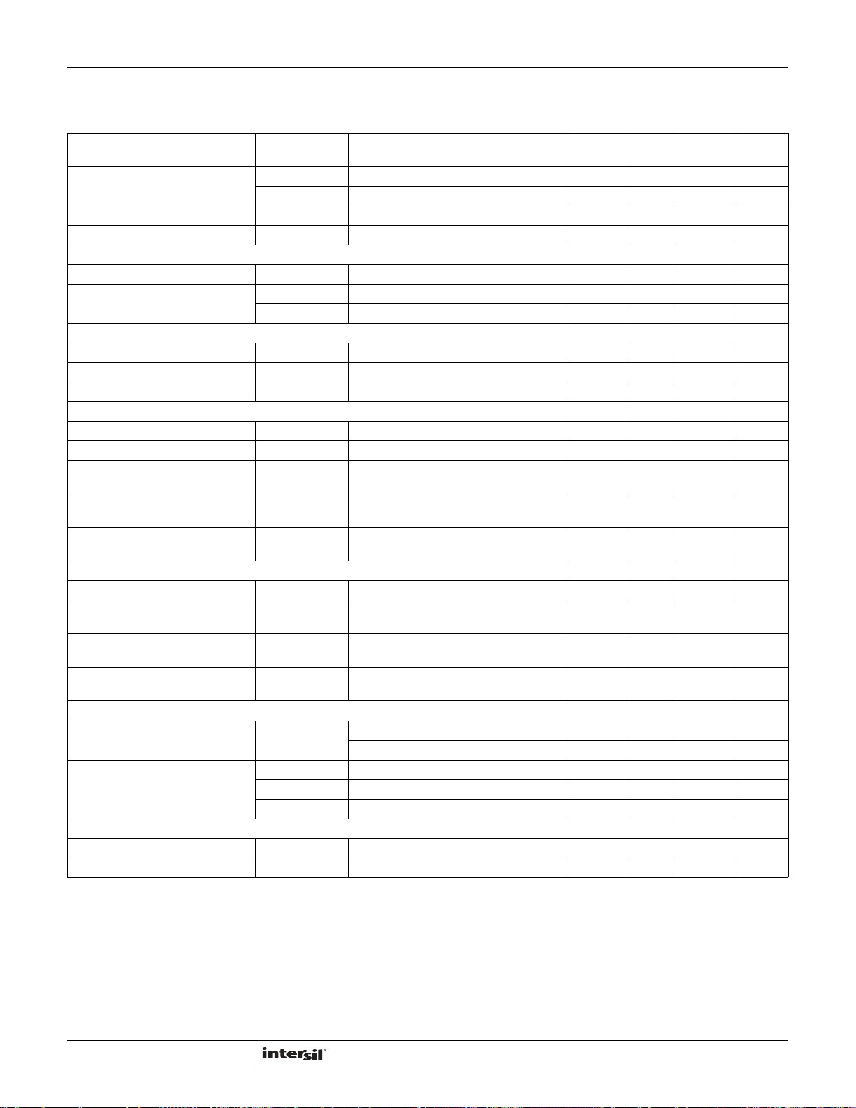
VR1 Overcurrent Threshold 3-Phase - PS0 and 1-Phase - all states 25.5 30.6 35.5 µA
3-Phase - PS1, 2-Phase - PS0 16.75 20.6 24.25 µA
3-Phase - PS2, 2-Phase - PS1 and PS2 8.5 10.6 12.75 µA
VR2 Overcurrent Threshold All states 28.5 30.6 33.5 µA
LOGIC THRESHOLDS
VR_ON Input Low V
VR_ON Input High V
PWM
PWM Output Low V
PWM Output High V
PWM Tri-State Leakage PWM = 2.5V 2 µA
THERMAL MONITOR
NTC Source Current NTC = 1.3V 59 60 61 µA
VR_HOT# Trip Voltage (VR1 and VR2) Falling 0.86 0.873 0.89 V
VR_HOT# Reset Voltage (VR1
and VR2)
Therm_Alert Trip Voltage (VR1
and VR2)
Therm_Alert Reset Voltage (VR1
and VR2)
CURRENT MONITOR
IMON Output Current (VR1 and VR2) ISUM- pin current = 25µA 147 150 153 µA
IMON Current Sinking Capability
(VR1 and VR2)
IccMax_Alert Trip Voltage (VR1
and VR2)
IccMax_Alert Reset Voltage (VR1
and VR2)
IL
IH
V
IH
0L
0H
HRTZ 0.7 V
IRTZ 0.75 V
Sinking 5mA 1.0 V
Sourcing 5mA 3.5 4.2 V
Rising 0.905 0.929 0.935 V
Falling 0.9 0.913 0.93 V
Rising 0.945 0.961 0.975 V
Rising 2.63 2.66 2.69 V
Falling 2.585 2.62 2.655 V
MIN
(Note 6) TYP
370 µA
MAX
(Note 6) UNITS
0.3 V
INPUTS
VR_ON Leakage Current I
SCLK, SDA Leakage VR_ON = 0V, SCLK & SDA = 0V & 1V -1 1 µA
SLEW RATE (For VID Change)
Fast Slew Rate 10 mV/µs
Slow Slew Rate 2.5 mV/µs
NOTES:
6. Compliance to datasheet limits is assured by one or more methods: production test, characterization and/or design.
VR_ON
VR_ON = 0V -1 0µA
VR_ON = 1V 18 35 µA
VR_ON = 1V, SCLK & SDA = 1V -5 1 µA
VR_ON = 1V, SCLK & SDA = 0V -85 -60 -30 µA
11
FN7613.0
January 21, 2011
Page 12

Gate Driver Timing Diagram
PWM
t
LGFUGR
UGATE
t
RU
ISL95831
t
FU
1V
LGATE
t
FL
1V
Theory of Operation
Multiphase R3™ Modulator
MASTER CLOCK CIRCUIT
gmVo
Crs1
Crs2
Crs3
MASTER
CLOCK
Vcrs1
Vcrs2
Vcrs3
VW
COMP
Vcrm
Crm
VW
VW
VW
MASTER
CLOCK
SLAVE CIRCUIT 1
Clock1
gm
SLAVE CIRCUIT 2
Clock2
gm
SLAVE CIRCUIT 3
Clock3
gm
S
Q
R
S
Q
R
S
Q
R
Phase
Sequencer
PWM1
PWM2
PWM3
Phase1
Phase2
Phase3
Clock1
Clock2
Clock3
L1
I
L1
L2
I
L2
L3
I
L3
Vo
Co
t
UGFLGR
t
VW
Vcrm
COMP
Master
Clock
Clock1
PWM1
Clock2
PWM2
Clock3
PWM3
FIGURE 4. R
RL
VW
Vcrs3
Vcrs2 V crs1
3
™ MODULATOR OPERATION PRINCIPLES IN
STEADY STATE
Hysteretic
Window
FIGURE 3. R
3
™ MODULATOR CIRCUIT
12
FN7613.0
January 21, 2011
Page 13
ISL95831
VW
COMP
Vcrm
Master
Clock
Clock1
PWM1
Clock2
PWM2
Clock3
PWM3
VW
Vcrs1
Vcrs3
Vcrs2
FIGURE 5. R
3
™ MODULATOR OPERATION PRINCIPLES IN LOAD
INSERTION RESPONSE
The ISL95831 is a multiphase regulator implementing Intel™
IMVP-7/VR12™ protocol. It has two voltage regulators, VR1 and
VR2, on one chip. VR1 can be programmed for 1-, 2- or 3-phase
operation, and VR2 is dedicated to 1-phase operation. The
following description is based on VR1, but also applies to VR2
because they are based on the same architecture.
3
The ISL95831 uses Intersil patented R
Regulator™) modulator. The R
3
™ modulator combines the best
™ (Robust Ripple
features of fixed frequency PWM and hysteretic PWM while
eliminating many of their shortcomings. Figure 3 conceptually
shows the multiphase R
3
™ modulator circuit, and Figure 4 shows
the operation principles.
Each slave circuit has its own ripple capacitor C
, whose voltage
rs
mimics the inductor ripple current. A gm amplifier converts the
inductor voltage into a current source to charge and discharge
. The slave circuit turns on its PWM pulse upon receiving the
C
rs
clock signal, and the current source charges Crs. When Crs
voltage V
and the current source discharges C
Since the controller works with V
hits VW, the slave circuit turns off the PWM pulse,
Crs
.
rs
, which are large-amplitude
crs
and noise-free synthesized signals, it achieves lower phase jitter
than conventional hysteretic mode and fixed PWM mode
controllers. Unlike conventional hysteretic mode converters, the
ISL95831 uses an error amplifier that allows the controller to
maintain a 0.5% output voltage accuracy.
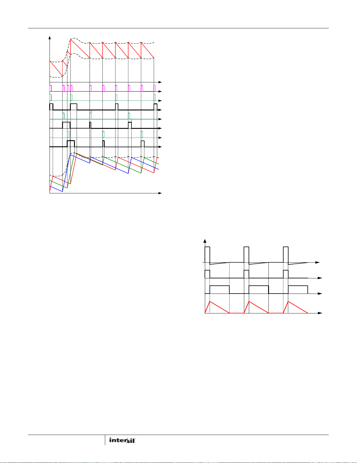
Figure 5 shows the operation principles during load insertion
response. The COMP voltage rises during load insertion,
generating the master clock signal more quickly, so the PWM
pulses turn on earlier, increasing the effective switching
frequency, which allows for higher control loop bandwidth than
conventional fixed frequency PWM controllers. The VW voltage
rises as the COMP voltage rises, making the PWM pulses wider.
During load release response, the COMP voltage falls. It takes
the master clock circuit longer to generate the next master clock
signal so the PWM pulse is held off until needed. The VW voltage
falls as the COMP voltage falls, reducing the current PWM pulse
width. This kind of behavior gives the controller excellent
response speed.
The fact that all the phases share the same VW window voltage
also ensures excellent dynamic current balance among phases.
Diode Emulation and Period Stretching
Phase
UGATE
LGATE
A current source flows from the VW pin to the COMP pin, creating
a voltage window set by the resistor between the two pins. This
voltage window is called VW window in the following discussion.
Inside the IC, the modulator uses the master clock circuit to
generate the clocks for the slave circuits. The modulator
discharges the ripple capacitor C
to g
, where gm is a gain factor. Crm voltage V
mVo
with a current source equal
rm
crm
is a
sawtooth waveform traversing between the VW and COMP
voltages. It resets to VW when it hits COMP, and generates a
one-shot master clock signal. A phase sequencer distributes the
master clock signal to the slave circuits. If VR1 is in 3-phase
mode, the master clock signal will be distributed to the three
phases, and the Clock1~3 signals will be 120° out-of-phase. If
VR1 is in 2-phase mode, the master clock signal will be
distributed to Phases 1 and 2, and the Clock1 and Clock2 signals
will be 180° out-of-phase. If VR1 is in 1-phase mode, the master
clock signal will be distributed to Phases 1 only and be the
Clock1 signal.
13
IL
FIGURE 6. DIODE EMULATION
ISL95831 can operate in diode emulation (DE) mode to improve
light load efficiency. In DE mode, the low-side MOSFET conducts
when the current is flowing from source to drain and doesn’t allow
reverse current, emulating a diode. As Figure 6 shows, when
LGATE is on, the low-side MOSFET carries current, creating
negative voltage on the phase node due to the voltage drop across
the ON-resistance. The controller monitors the current through
monitoring the phase node voltage. It turns off LGATE when the
phase node voltage reaches zero to prevent the inductor current
from reversing the direction and creating unnecessary power loss.
If the load current is light enough, as Figure 6 shows, the inductor
current will reach and stay at zero before the next phase node
pulse and the regulator is in discontinuous conduction mode
(DCM). If the load current is heavy enough, the inductor current
FN7613.0
January 21, 2011
Page 14

ISL95831
will never reach 0A, and the regulator is in CCM although the
controller is in DE mode.
Figure 7 shows the operation principle in diode emulation mode at
light load. The load gets incrementally lighter in the three cases
from top to bottom. The PWM on-time is determined by the VW
window size, therefore is the same, making the inductor current
triangle the same in the three cases. The controller clamps the
ripple capacitor voltage V
inductor current. It takes the COMP voltage longer to hit V
in DE mode to make it mimic the
crs
crs
,
naturally stretching the switching period. The inductor current
triangles move further apart from each other such that the
inductor current average value is equal to the load current. The
reduced switching frequency helps increase light load efficiency.
CCM/DCM BOUNDARY
VW
Vcrs
iL
LIGHT DCM
Vcrs
iL
Vcrs
iL
VW
DEEP DCM
VW
FIGURE 7. PERIOD STRETCHING
Start-up Timing
With the controller's VDD voltage above the POR threshold, the
start-up sequence begins when VR_ON exceeds the logic high
threshold. Figure 8 shows the typical start-up timing of VR1 and
VR2. The controller uses digital soft-start to ramp-up DAC to the
voltage programmed by the SetVID command. PGOOD is asserted
high and ALERT# is asserted low at the end of the ramp up. Similar
results occur if VR_ON is tied to V
starting 800µs after V
VDD
VR_ON
DAC
PGOOD
ALERT#
FIGURE 8. VR1 SOFT-START WAVEFORMS
crosses the POR threshold.
DD
2.5mV/µs
800µs
, with the soft-start sequence
DD
SLEW RATE
VID
…...
VID
COMMAND
VOLTAGE
Voltage Regulation and Load Line
Implementation
After the start sequence, the controller regulates the output
voltage to the value set by the VID information per Table 1. The
controller will control the no-load output voltage to an accuracy of
±0.5% over the range of 0.75V to 1.52V. A differential amplifier
allows voltage sensing for precise voltage regulation at the
microprocessor die.
TABLE 1. VID TABLE
VID
Hex V
0 0 0 0 0 0 0 0 0 0 0.00000
0 0 0 0 0 0 0 1 0 1 0.25000
0 0 0 0 0 0 1 0 0 2 0.25500
0 0 0 0 0 0 1 1 0 3 0.26000
0 0 0 0 0 1 0 0 0 4 0.26500
0 0 0 0 0 1 0 1 0 5 0.27000
0 0 0 0 0 1 1 0 0 6 0.27500
0 0 0 0 0 1 1 1 0 7 0.28000
0 0 0 0 1 0 0 0 0 8 0.28500
0 0 0 0 1 0 0 1 0 9 0.29000
0 0 0 0 1 0 1 0 0 A 0.29500
0 0 0 0 1 0 1 1 0 B 0.30000
0 0 0 0 1 1 0 0 0 C 0.30500
000 011010D0.31000
0 0 0 0 1 1 1 0 0 E 0.31500
0 0 0 0 1 1 1 1 0 F 0.32000
0 0 0 1 0 0 0 0 1 0 0.32500
0 0 0 1 0 0 0 1 1 1 0.33000
0 0 0 1 0 0 1 0 1 2 0.33500
0 0 0 1 0 0 1 1 1 3 0.34000
0 0 0 1 0 1 0 0 1 4 0.34500
0 0 0 1 0 1 0 1 1 5 0.35000
0 0 0 1 0 1 1 0 1 6 0.35500
0 0 0 1 0 1 1 1 1 7 0.36000
0 0 0 1 1 0 0 0 1 8 0.36500
0 0 0 1 1 0 0 1 1 9 0.37000
0 0 0 1 1 0 1 0 1 A 0.37500
0 0 0 1 1 0 1 1 1 B 0.38000
0 0 0 1 1 1 0 0 1 C 0.38500
0 0 0 1 1 1 0 1 1 D 0.39000
0 0 0 1 1 1 1 0 1 E 0.39500
0 0 0 1 1 1 1 1 1 F 0.40000
(V)765 43210
O
14
FN7613.0
January 21, 2011
Page 15

ISL95831
TABLE 1. VID TABLE
VID
0 0 1 0 0 0 0 0 2 0 0.40500
001 00001210.41000
0 0 1 0 0 0 1 0 2 2 0.41500
0 0 1 0 0 0 1 1 2 3 0.42000
0 0 1 0 0 1 0 0 2 4 0.42500
0 0 1 0 0 1 0 1 2 5 0.43000
0 0 1 0 0 1 1 0 2 6 0.43500
0 0 1 0 0 1 1 1 2 7 0.44000
0 0 1 0 1 0 0 0 2 8 0.44500
0 0 1 0 1 0 0 1 2 9 0.45000
0 0 1 0 1 0 1 0 2 A 0.45500
0 0 1 0 1 0 1 1 2 B 0.46000
0 0 1 0 1 1 0 0 2 C 0.46500
0 0 1 0 1 1 0 1 2 D 0.47000
0 0 1 0 1 1 1 0 2 E 0.47500
0 0 1 0 1 1 1 1 2 F 0.48000
0 0 1 1 0 0 0 0 3 0 0.48500
0 0 1 1 0 0 0 1 3 1 0.49000
0 0 1 1 0 0 1 0 3 2 0.49500
0 0 1 1 0 0 1 1 3 3 0.50000
0 0 1 1 0 1 0 0 3 4 0.50500
001 10101350.51000
0 0 1 1 0 1 1 0 3 6 0.51500
0 0 1 1 0 1 1 1 3 7 0.52000
0 0 1 1 1 0 0 0 3 8 0.52500
0 0 1 1 1 0 0 1 3 9 0.53000
0 0 1 1 1 0 1 0 3 A 0.53500
001 110113B0.54000
001 111003C0.54500
0 0 1 1 1 1 0 1 3 D 0.55000
0 0 1 1 1 1 1 0 3 E 0.55500
0 0 1 1 1 1 1 1 3 F 0.56000
0 1 0 0 0 0 0 0 4 0 0.56500
0 1 0 0 0 0 0 1 4 1 0.57000
0 1 0 0 0 0 1 0 4 2 0.57500
0 1 0 0 0 0 1 1 4 3 0.58000
0 1 0 0 0 1 0 0 4 4 0.58500
0 1 0 0 0 1 0 1 4 5 0.59000
0 1 0 0 0 1 1 0 4 6 0.59500
(Continued)
Hex V
(V)765 43210
O
TABLE 1. VID TABLE
VID
0 1 0 0 0 1 1 1 4 7 0.60000
0 1 0 0 1 0 0 0 4 8 0.60500
010 01001490.61000
0 1 0 0 1 0 1 0 4 A 0.61500
0 1 0 0 1 0 1 1 4 B 0.62000
0 1 0 0 1 1 0 0 4 C 0.62500
0 1 0 0 1 1 0 1 4 D 0.63000
0 1 0 0 1 1 1 0 4 E 0.63500
0 1 0 0 1 1 1 1 4 F 0.64000
0 1 0 1 0 0 0 0 5 0 0.64500
0 1 0 1 0 0 0 1 5 1 0.65000
0 1 0 1 0 0 1 0 5 2 0.65500
0 1 0 1 0 0 1 1 5 3 0.66000
0 1 0 1 0 1 0 0 5 4 0.66500
0 1 0 1 0 1 0 1 5 5 0.67000
0 1 0 1 0 1 1 0 5 6 0.67500
0 1 0 1 0 1 1 1 5 7 0.68000
0 1 0 1 1 0 0 0 5 8 0.68500
0 1 0 1 1 0 0 1 5 9 0.69000
0 1 0 1 1 0 1 0 5 A 0.69500
0 1 0 1 1 0 1 1 5 B 0.70000
0 1 0 1 1 1 0 0 5 C 0.70500
010 111015D0.71000
010 111105E0.71500
0 1 0 1 1 1 1 1 5 F 0.72000
0 1 1 0 0 0 0 0 6 0 0.72500
0 1 1 0 0 0 0 1 6 1 0.73000
0 1 1 0 0 0 1 0 6 2 0.73500
0 1 1 0 0 0 1 1 6 3 0.74000
0 1 1 0 0 1 0 0 6 4 0.74500
0 1 1 0 0 1 0 1 6 5 0.75000
0 1 1 0 0 1 1 0 6 6 0.75500
0 1 1 0 0 1 1 1 6 7 0.76000
0 1 1 0 1 0 0 0 6 8 0.76500
0 1 1 0 1 0 0 1 6 9 0.77000
0 1 1 0 1 0 1 0 6 A 0.77500
0 1 1 0 1 0 1 1 6 B 0.78000
0 1 1 0 1 1 0 0 6 C 0.78500
0 1 1 0 1 1 0 1 6 D 0.79000
(Continued)
Hex V
(V)765 43210
O
15
FN7613.0
January 21, 2011
Page 16

ISL95831
TABLE 1. VID TABLE
VID
0 1 1 0 1 1 1 0 6 E 0.79500
0 1 1 0 1 1 1 1 6 F 0.80000
0 1 1 1 0 0 0 0 7 0 0.80500
011 10001710.81000
0 1 1 1 0 0 1 0 7 2 0.81500
0 1 1 1 0 0 1 1 7 3 0.82000
0 1 1 1 0 1 0 0 7 4 0.82500
0 1 1 1 0 1 0 1 7 5 0.83000
0 1 1 1 0 1 1 0 7 6 0.83500
0 1 1 1 0 1 1 1 7 7 0.84000
0 1 1 1 1 0 0 0 7 8 0.84500
0 1 1 1 1 0 0 1 7 9 0.85000
0 1 1 1 1 0 1 0 7 A 0.85500
0 1 1 1 1 0 1 1 7 B 0.86000
0 1 1 1 1 1 0 0 7 C 0.86500
0 1 1 1 1 1 0 1 7 D 0.87000
0 1 1 1 1 1 1 0 7 E 0.87500
0 1 1 1 1 1 1 1 7 F 0.88000
1 0 0 0 0 0 0 0 8 0 0.88500
1 0 0 0 0 0 0 1 8 1 0.89000
1 0 0 0 0 0 1 0 8 2 0.89500
1 0 0 0 0 0 1 1 8 3 0.90000
1 0 0 0 0 1 0 0 8 4 0.90500
100 00101850.91000
1 0 0 0 0 1 1 0 8 6 0.91500
1 0 0 0 0 1 1 1 8 7 0.92000
1 0 0 0 1 0 0 0 8 8 0.92500
1 0 0 0 1 0 0 1 8 9 0.93000
1 0 0 0 1 0 1 0 8 A 0.93500
1 0 0 0 1 0 1 1 8 B 0.94000
1 0 0 0 1 1 0 0 8 C 0.94500
1 0 0 0 1 1 0 1 8 D 0.95000
1 0 0 0 1 1 1 0 8 E 0.95500
1 0 0 0 1 1 1 1 8 F 0.96000
1 0 0 1 0 0 0 0 9 0 0.96500
1 0 0 1 0 0 0 1 9 1 0.97000
1 0 0 1 0 0 1 0 9 2 0.97500
1 0 0 1 0 0 1 1 9 3 0.98000
1 0 0 1 0 1 0 0 9 4 0.98500
(Continued)
Hex V
(V)765 43210
O
TABLE 1. VID TABLE
VID
1 0 0 1 0 1 0 1 9 5 0.99000
1 0 0 1 0 1 1 0 9 6 0.99500
1 0 0 1 0 1 1 1 9 7 1.00000
1 0 0 1 1 0 0 0 9 8 1.00500
100 11001991.01000
1 0 0 1 1 0 1 0 9 A 1.01500
1 0 0 1 1 0 1 1 9 B 1.02000
1 0 0 1 1 1 0 0 9 C 1.02500
1 0 0 1 1 1 0 1 9 D 1.03000
1 0 0 1 1 1 1 0 9 E 1.03500
1 0 0 1 1 1 1 1 9 F 1.04000
1 0 1 0 0 0 0 0 A 0 1.04500
1 0 1 0 0 0 0 1 A 1 1.05000
1 0 1 0 0 0 1 0 A 2 1.05500
1 0 1 0 0 0 1 1 A 3 1.06000
1 0 1 0 0 1 0 0 A 4 1.06500
101 00101A51.07000
101 00110A61.07500
1 0 1 0 0 1 1 1 A 7 1.08000
1 0 1 0 1 0 0 0 A 8 1.08500
1 0 1 0 1 0 0 1 A 9 1.09000
1 0 1 0 1 0 1 0 A A 1.09500
1 0 1 0 1 0 1 1 A B 1.10000
1 0 1 0 1 1 0 0 A C 1.10500
101 01101AD1.11000
1 0 1 0 1 1 1 0 A E 1.11500
1 0 1 0 1 1 1 1 A F 1.12000
1 0 1 1 0 0 0 0 B 0 1.12500
1 0 1 1 0 0 0 1 B 1 1.13000
1 0 1 1 0 0 1 0 B 2 1.13500
1 0 1 1 0 0 1 1 B 3 1.14000
1 0 1 1 0 1 0 0 B 4 1.14500
1 0 1 1 0 1 0 1 B 5 1.15000
1 0 1 1 0 1 1 0 B 6 1.15500
1 0 1 1 0 1 1 1 B 7 1.16000
1 0 1 1 1 0 0 0 B 8 1.16500
1 0 1 1 1 0 0 1 B 9 1.17000
1 0 1 1 1 0 1 0 B A 1.17500
1 0 1 1 1 0 1 1 B B 1.18000
(Continued)
Hex V
(V)765 43210
O
16
FN7613.0
January 21, 2011
Page 17

ISL95831
TABLE 1. VID TABLE
VID
1 0 1 1 1 1 0 0 B C 1.18500
1 0 1 1 1 1 0 1 B D 1.19000
1 0 1 1 1 1 1 0 B E 1.19500
101 11111BF1.20000
110 00000C01.20500
110 00001C11.21000
1 1 0 0 0 0 1 0 C 2 1.21500
110 00011C31.22000
110 00100C41.22500
110 00101C51.23000
110 00110C61.23500
1 1 0 0 0 1 1 1 C 7 1.24000
1 1 0 0 1 0 0 0 C 8 1.24500
110 01001C91.25000
110 01010CA1.25500
110 01011CB1.26000
110 01100CC1.26500
1 1 0 0 1 1 0 1 C D 1.27000
1 1 0 0 1 1 1 0 C E 1.27500
110 01111CF1.28000
110 10000D01.28500
110 10001D11.29000
110 10010D21.29500
110 10011D31.30000
110 10100D41.30500
110 10101D51.31000
110 10110D61.31500
110 10111D71.32000
110 11000D81.32500
110 11001D91.33000
110 11010DA1.33500
110 11011DB1.34000
110 11100DC1.34500
110 11101DD1.35000
110 11110DE1.35500
110 11111DF1.36000
111 00000E01.36500
1 1 1 0 0 0 0 1 E 1 1.37000
1 1 1 0 0 0 1 0 E 2 1.37500
(Continued)
Hex V
(V)765 43210
O
TABLE 1. VID TABLE
VID
1 1 1 0 0 0 1 1 E 3 1.38000
1 1 1 0 0 1 0 0 E 4 1.38500
1 1 1 0 0 1 0 1 E 5 1.39000
1 1 1 0 0 1 1 0 E 6 1.39500
1 1 1 0 0 1 1 1 E 7 1.40000
1 1 1 0 1 0 0 0 E 8 1.40500
111 01001E91.41000
1 1 1 0 1 0 1 0 E A 1.41500
1 1 1 0 1 0 1 1 E B 1.42000
1 1 1 0 1 1 0 0 E C 1.42500
1 1 1 0 1 1 0 1 E D 1.43000
1 1 1 0 1 1 1 0 E E 1.43500
1 1 1 0 1 1 1 1 E F 1.44000
1 1 1 1 0 0 0 0 F 0 1.44500
1 1 1 1 0 0 0 1 F 1 1.45000
1 1 1 1 0 0 1 0 F 2 1.45500
1 1 1 1 0 0 1 1 F 3 1.46000
1 1 1 1 0 1 0 0 F 4 1.46500
1 1 1 1 0 1 0 1 F 5 1.47000
1 1 1 1 0 1 1 0 F 6 1.47500
1 1 1 1 0 1 1 1 F 7 1.48000
1 1 1 1 1 0 0 0 F 8 1.48500
1 1 1 1 1 0 0 1 F 9 1.49000
1 1 1 1 1 0 1 0 F A 1.49500
1 1 1 1 1 0 1 1 F B 1.50000
1 1 1 1 1 1 0 0 F C 1.50500
111 11101FD1.51000
1 1 1 1 1 1 1 0 F E 1.51500
1 1 1 1 1 1 1 1 F F 1.52000
(Continued)
Hex V
(V)765 43210
O
17
FN7613.0
January 21, 2011
Page 18
ISL95831
Rdroop
Σ
Idroop
VDAC
Vdroop
DAC
X 1
VIDs
RTN
VSS
FB
COMP
FIGURE 9. DIFFERENTIAL SENSING AND LOAD LINE
E/A
INTERNAL TO IC
IMPLEMENTATION
VCC
“CATCH”
RESISTOR
VID
VSS
“CATCH” RESISTOR
SENSE
VR LOCAL VO
SENSE
As the load current increases from zero, the output voltage will
droop from the VID table value by an amount proportional to the
load current to achieve the load line. The controller can sense the
inductor current through the intrinsic DC Resistance (DCR) of the
inductors (as shown in Figure 1) or through resistors in series
with the inductors (as shown in Figure 2). In both methods,
capacitor C
voltage represents the inductor total currents. A
n
droop amplifier converts Cn voltage into an internal current
source with the gain set by resistor R
. The current source is used
i
for load line implementation, current monitor and overcurrent
protection.
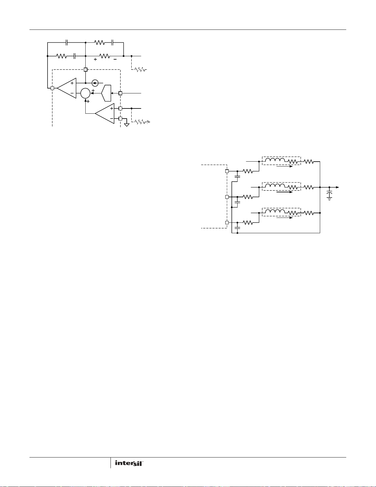
Figure 9 shows the load line implementation. The controller
drives a current source I
out of the FB pin, described by
droop
Equation 1.
I
droop
=
----------------
R
i
Cn
(EQ. 1)
2xV
When using inductor DCR current sensing, a single NTC element
is used to compensate the positive temperature coefficient of the
copper winding thus sustaining the load line accuracy with
reduced cost.
flows through resistor R
I
droop
and creates a voltage drop,
droop
as shown in Equation 2.
V
droopRdroopIdroop
is the droop voltage required to implement load line.
V
droop
Changing R
slope. Since I
recommended to first scale I
then select an appropriate R
×=
or scaling I
droop
also sets the overcurrent protection level, it is
droop
can both change the load line
droop
based on OCP requirement,
droop
value to obtain the desired
droop
(EQ. 2)
load line slope.
Differential Voltage Sensing
Figure 9 also shows the differential voltage sensing scheme.
VCC
from the processor die. A unity gain differential amplifier senses
the VSS
amplifier regulates the inverting and the non-inverting input
voltages to be equal, as shown in Equation 3:
Rewriting Equation 3 and substitution of Equation 2 gives:
SENSE
SENSE
and VSS
are the remote voltage sensing signals
SENSE
voltage and adds it to the DAC output. The error
VCC
VCC
SENSE
– V
SENSE
V+
droop
VSS
SENSE
V
VSS
+=
DAC
SENSE
DACRdroopIdroop
×–=
(EQ. 3)
(EQ. 4)
Equation 4 is the exact equation required for load line
implementation.
The VCC
SENSE
and VSS
signals come from the processor die.
SENSE
The feedback will be open circuit in the absence of the processor. As
Figure 9 shows, it is recommended to add a “catch” resistor to feed
the VR local output voltage back to the compensator, and add
another “catch” resistor to connect the VR local output ground to the
RTN pin. These resistors, typically 10Ω~100Ω, will provide voltage
feedback if the system is powered up without a processor installed.
Phase Current Balancing
Rdcr3
L3
Phase3
ISEN3
INTERNAL
TO IC
ISEN2
ISEN1
Risen
Cisen
Phase2
Risen
Cisen
Phase1
Risen
Cisen
FIGURE 10. CURRENT BALANCING CIRCUIT
IL3
L2
IL2
L1
IL1
The controller monitors individual phase average current by
monitoring the ISEN1, ISEN2, and ISEN3 voltages. Figure 10
shows the recommended current balancing circuit. Each phase
node voltage is averaged by a low-pass filter consisting of R
and C
, and presented to the corresponding ISEN pin. R
isen
should be routed to inductor phase-node pad in order to
eliminate the effect of phase node parasitic PCB DCR. Equations
5 thru 7 give the ISEN pin voltages:
V
ISEN1
V
ISEN2
V
ISEN3
where R
and R
R
+()IL1×=
dcr1Rpcb1
R
+()IL2×=
dcr2Rpcb2
R
+()IL3×=
dcr3Rpcb3
, R
dcr2
and R
dcr1
are parasitic PCB DCR between the inductor output
pcb3
are inductor DCR; R
dcr3
side pad and the output voltage rail; and I
inductor average currents.
The controller will adjust the phase pulse-width relative to the
other phases to make V
I
L1=IL2=IL3
R
pcb1=Rpcb2=Rpcb3
, when there are R
ISEN1=VISEN2=VISEN3
dcr1=Rdcr2=Rdcr3
.
Using the same components for L1, L2 and L3 will provide a good
match of R
dcr1
, R
dcr2
and R
. Board layout will determine
dcr3
Rpcb3
Rdcr2
Rpcb2
Rdcr1
Rpcb1
pcb1
, IL2 and IL3 are
L1
, thus to achieve
, R
and
V
o
isen
isen
(EQ. 5)
(EQ. 6)
(EQ. 7)
pcb2
18
FN7613.0
January 21, 2011
Page 19
ISL95831
R
, R
pcb2
and R
pcb1
layout for the power delivery path between each inductor and the
output voltage rail, such that R
ISEN3
Cisen
INTERNAL
TO IC
ISEN2
ISEN1
FIGURE 11. DIFFERENTIAL-SENSING CURRENT BALANCING
Phase2
Cisen
Cisen
CIRCUIT
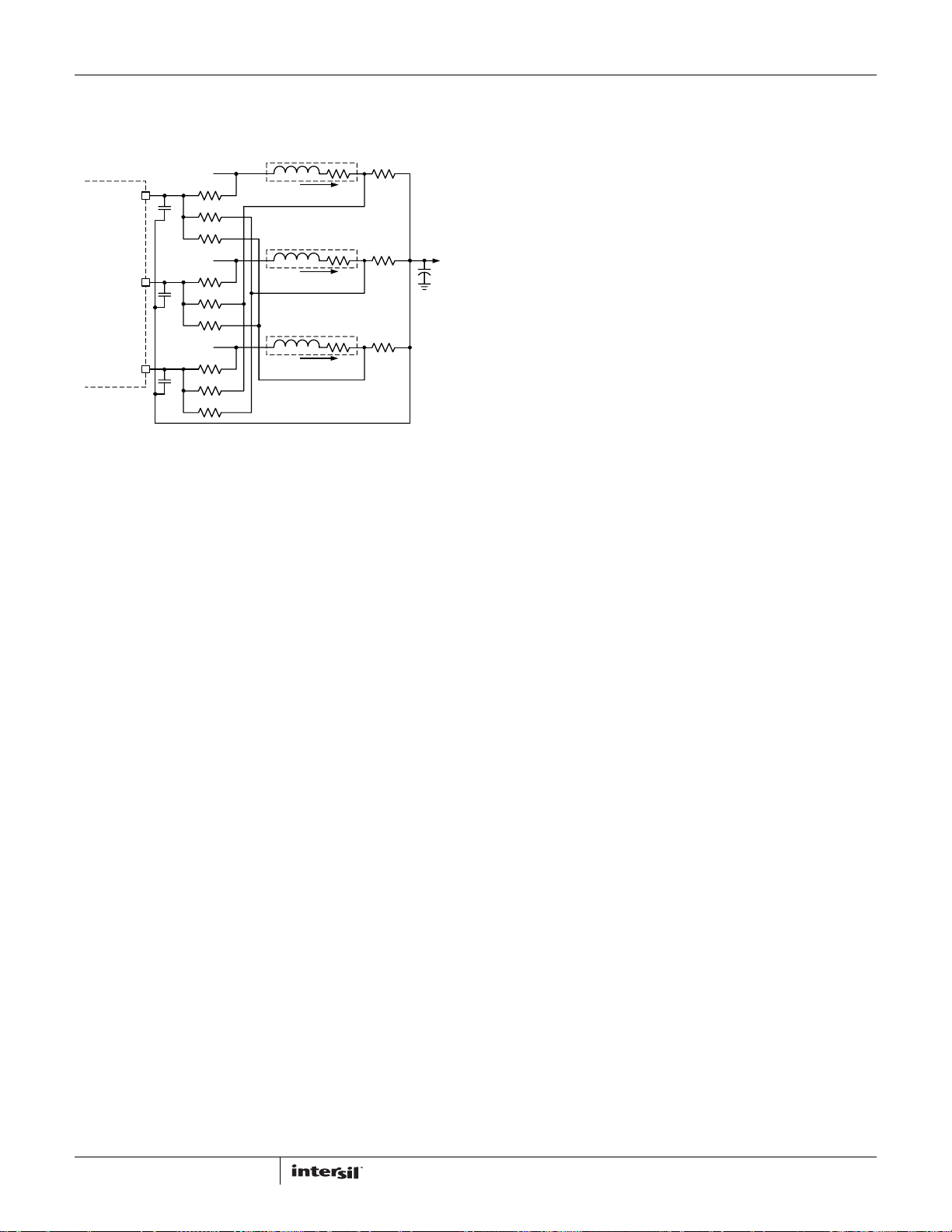
Sometimes, it is difficult to implement symmetrical layout. For
the circuit shown in Figure 10, asymmetric layout causes
different R
pcb1
, R
11 shows a recommended differential-sensing current balancing
circuit. The current sensing traces should be routed to the
inductor pads so they only pick up the inductor DCR voltage. Each
ISEN pin sees the average voltage of three sources: its own phase
inductor phase-node pad, and the other two phases inductor
output side pads. Equations 8 thru 10 give the ISEN pin voltages:
V
ISEN1V1pV2nV3n
++=
. It is recommended to have symmetrical
pcb3
pcb1=Rpcb2=Rpcb3
Rdcr3
L3
IL3
V3n
Rdcr2
L2
IL2
V2n
L1
Rdcr1
IL1
V1n
thus current imbalance. Figure
pcb3
Phase3
Risen
Risen
Risen
Risen
Risen
Risen
Phase1
Risen
Risen
Risen
pcb2
V3p
V2p
V1p
and R
.
Rpcb3
Rpcb2
Rpcb1
V
o
(EQ. 8)
V
ISEN2V1nV2pV3n
V
ISEN3V1nV2nV3p
The controller will make V
++=
++=
ISEN1
= V
ISEN2
= V
ISEN3
(EQ. 9)
(EQ. 10)
, as shown in
Equations 11 and 12:
++ V1nV2pV
V
1pV2nV3n
++ V1nV2nV
V
1nV2pV3n
++=
++=
3n
3p
(EQ. 11)
(EQ. 12)
Rewriting Equation 11 gives Equation 13:
V
– V2pV2n–=
1pV1n
(EQ. 13)
and rewriting Equation 12 gives Equation 14:
V
– V3pV3n–=
2pV2n
(EQ. 14)
Combining Equations 13 and 14 gives:
– V2pV2n– V3pV3n–==
V
1pV1n
(EQ. 15)
Therefore:
R
× R
dcr1IL1
Current balancing (I
R
dcr1=Rdcr2=Rdcr3
× R
dcr2IL2
L1=IL2=IL3
. R
pcb1
×==
dcr3IL3
(EQ. 16)
) will be achieved when there is
, R
pcb2
and R
will not have any
pcb3
effect.
Since the slave ripple capacitor voltages mimic the inductor currents,
3
™ modulator can naturally achieve excellent current balancing
R
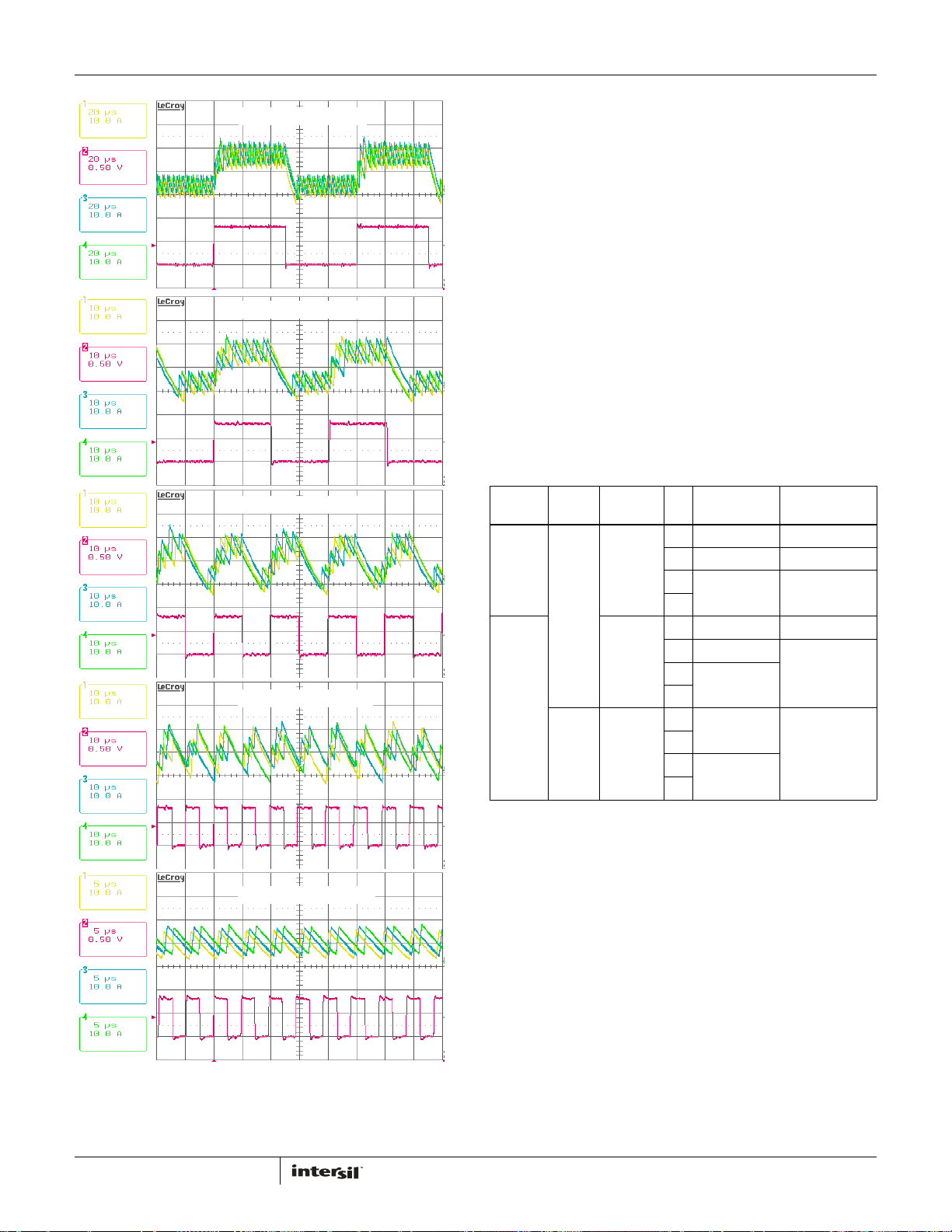
during steady state and dynamic operations. Figure 12 shows current
balancing performance of the evaluation board with load transient of
12A/51A at different rep rates. The inductor currents follow the load
current dynamic change with the output capacitors supplying the
difference. The inductor currents can track the load current well at low
rep rate, but cannot keep up when the rep rate gets into the
hundred-kHz range, where it’s out of the control loop bandwidth. The
controller achieves excellent current balancing in all cases.
19
FN7613.0
January 21, 2011
Page 20
ISL95831
7
REP RATE = 10kHz
REP RATE = 25kHz
REP RATE = 50kHz
REP RATE = 100kHz
CCM Switching Frequency
The R
sets the VW windows size, therefore sets the switching frequency.
When the ISL95831 is in continuous conduction mode (CCM), the
switching frequency is not absolutely constant due to the nature
of the R
Modulator” on page 12, the effective switching frequency will
increase during load insertion and will decrease during load
release to achieve fast response. On the other hand, the
switching frequency is relatively constant at steady state.
Variation is expected when the power stage condition, such as
input voltage, output voltage, load, etc. changes. The variation is
usually less than 15% and doesn’t have any significant effect on
output voltage ripple magnitude. Equation 17 gives an estimate
of the frequency-setting resistor R
approximately 300kHz switching frequency. Lower resistance
gives higher switching frequency.
resistor between the COMP and the VW pins sets the
fset
3
™ modulator. As explained in the “Multiphase R3™
value. 8kΩ R
fset
R
kΩ() Period μs()0.29–()2.65×=
fset
fset
gives
(EQ. 1
Modes of Operation
TABLE 2. VR1 MODES OF OPERATION
OCP Threshold
PWM3 ISEN2 CONFIG. PS MODE
To
External
Driver
Tied to 5V 2-phase
To
Power
Stage
Tied to 5V1-phase
3-phase
CPU VR
Config.
CPU VR
Config.
CPU VR
Config.
0 3-phase CCM 60
1 2-phase CCM 40
2 1-phase DE 20
3
0 2-phase CCM 40
1 1-phase CCM 20
2 1-phase DE
3
0 1-phase CCM 60
1
2 1-phase DE
3
(µA)
REP RATE = 200kHz
FIGURE 12. CURRENT BALANCING DURING DYNAMIC
OPERATION. CH1: IL1, CH2: I
IL3
, CH3: IL2, CH4:
LOAD
20
VR1 can be configured for 3, 2 or 1-phase operation. Table 2
shows VR1 configurations and operational modes, programmed
by the PWM3 pin and the ISEN2 pin status, and the PS
command. For 2-phase configuration, tie the PWM3 pin to 5V. In
this configuration, phases 1 and 2 are active. For 1-phase
configuration, tie the PWM3 pin and the ISEN2 pin to 5V. In this
configuration, only phase-1 is active.
In 3-phase configuration, VR1 operates in 3-phase CCM in PS0. It
enters 2-phase CCM in PS1 by dropping phase 3 and reducing
the overcurrent and the way-overcurrent protection levels to 2/3
of the initial values. It enters 1-phase DE mode in PS2 or PS3 by
dropping phases 3 and 2, and reduces the overcurrent and the
way-overcurrent protection levels to 1/3 of the initial values.
In 2-phase configuration, VR1 operates in 2-phase CCM in PS0. It
enters 1-phase CCM in PS1 and enters 1-phase DE mode in PS2
or PS3 by dropping phase 2, and reducing the overcurrent and
the way-overcurrent protection levels to 1/2 of the initial values.
FN7613.0
January 21, 2011
Page 21
ISL95831
In 1-phase configuration, VR1 operates in 1-phase CCM in PS0
and PS1, and enters 1-phase DE mode in PS2 and PS3.
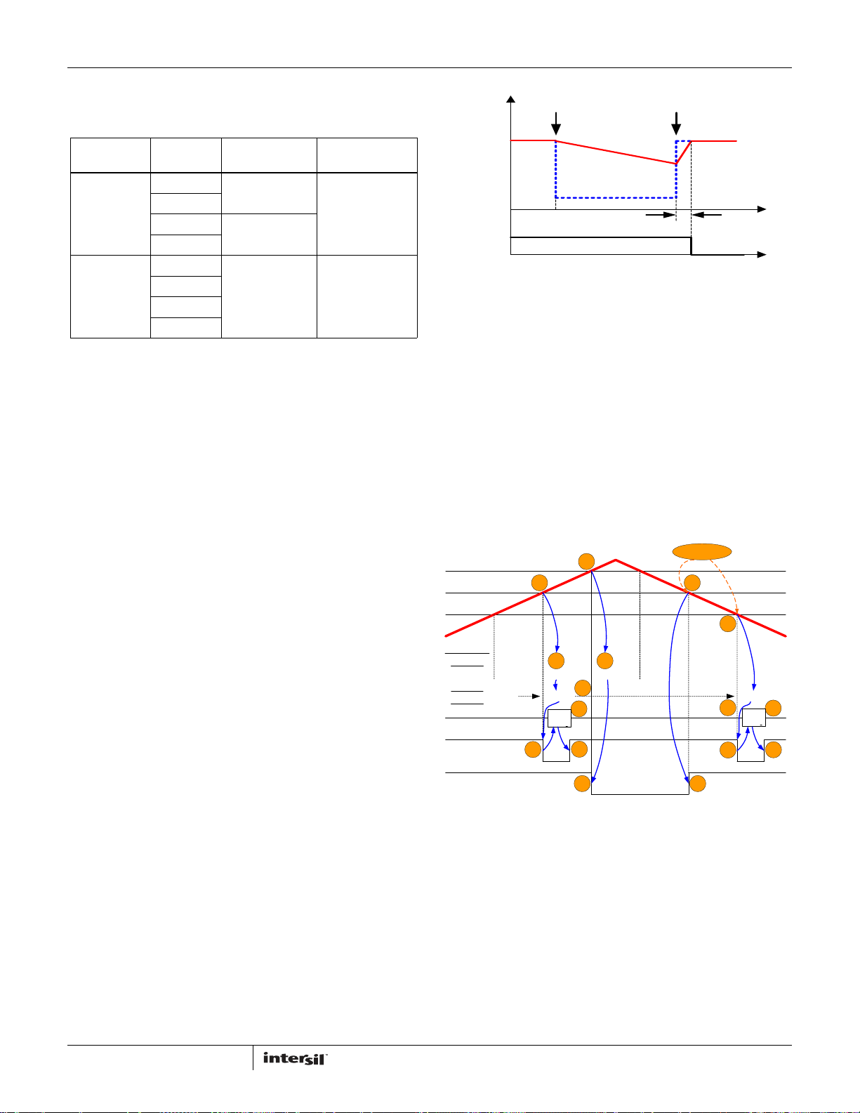
TABLE 3. VR2 MODES OF OPERATION
OCP Threshold
Rcompg PS MODE
Open Circuit 0 1-phase CCM 60
1
21-phase DE
3
100kΩ 01-phase DE 60
1
2
3
(µA)
Table 3 shows VR2 operational modes, programmed by the PS
command and Rcompg. Rcompg is a resistor connected between
the COMPG pin and GND. If Rcompg is equal to 100kΩ, VR2
operates in DE mode for all PS modes. If Rcompg is open circuit,
VR2 operates in 1-phase CCM in PS0 and PS1, and enters
1-phase DE mode in PS2 and PS3.
VR2 can be disabled completely by tying ISUMNG to 5V, and all
communication to VR2 will be rejected.
Dynamic Operation
VR1 and VR2 behave the same during dynamic operation. The
controller responds to VID changes by slewing to the new voltage
at a slew rate indicated in the SetVID command. There are three
SetVID slew rates, namely SetVID_fast, SetVID_slow and
SetVID_decay.
SetVID_fast command prompts the controller to enter CCM and
to actively drive the output voltage to the new VID value at a
minimum 10mV/µs slew rate.
SetVID_slow command prompts the controller to enter CCM and
to actively drive the output voltage to the new VID value at a
minimum 2.5mV/µs slew rate.
SetVID_decay command prompts the controller to enter DE
mode. The output voltage will decay down to the new VID value at
a slew rate determined by the load. If the voltage decay rate is
too fast, the controller will limit the voltage slew rate at
SetVID_slow slew rate.
ALERT# will be asserted low at the end of SetVID_fast and
SetVID_slow VID transitions.
SetVID_decay SetVID_fast/slow
Vo
VID
t1
ALERT#
FIGURE 13. SETVID DECAY PRE-EMPTIVE BEHAVIOR
T_alert
t3
t2
Figure 13 shows SetVID Decay Pre-Emptive behavior. The
controller receives a SetVID_decay command at t1. The VR
enters DE mode and the output voltage Vo decays down slowly.
At t2, before Vo reaches the intended VID target of the
SetVID_decay command, the controller receives a SetVID_fast (or
SetVID_slow) command to go to a voltage higher than the actual
Vo. The controller will turn around immediately and slew Vo to the
new target voltage at the slew rate specified by the SetVID
command. At t3, Vo reaches the new target voltage and the
controller asserts the ALERT# signal.
3™
The R
modulator intrinsically has voltage feed-forward. The
output voltage is insensitive to a fast slew rate input voltage
change.
VR_HOT#/ALERT# Behavior
2
GerReg
Status1
VR Temperature
7
8
3
5
6
9
Temp Zone
Bit 7 =1
Bit 6 =1
Bit 5 =1
Temp Zone
Register
0001 1111 0011 1111 0111 1111 1111 1111 0111 1111 0011 1111 0001 1111
Status 1
= “001” = “011” = “001”
Register
SVID
ALERT#
VR_HOT#
1
4
FIGURE 14. VR_HOT#/ALERT# BEHAVIOR
The controller drives 60µA current source out of the NTC pin and
the NTCG pin alternatively at 1kHz frequency with 50% duty
cycle. The current source flows through the respective NTC
resistor networks on the pins and creates voltages that are
monitored by the controller through an A/D converter (ADC) to
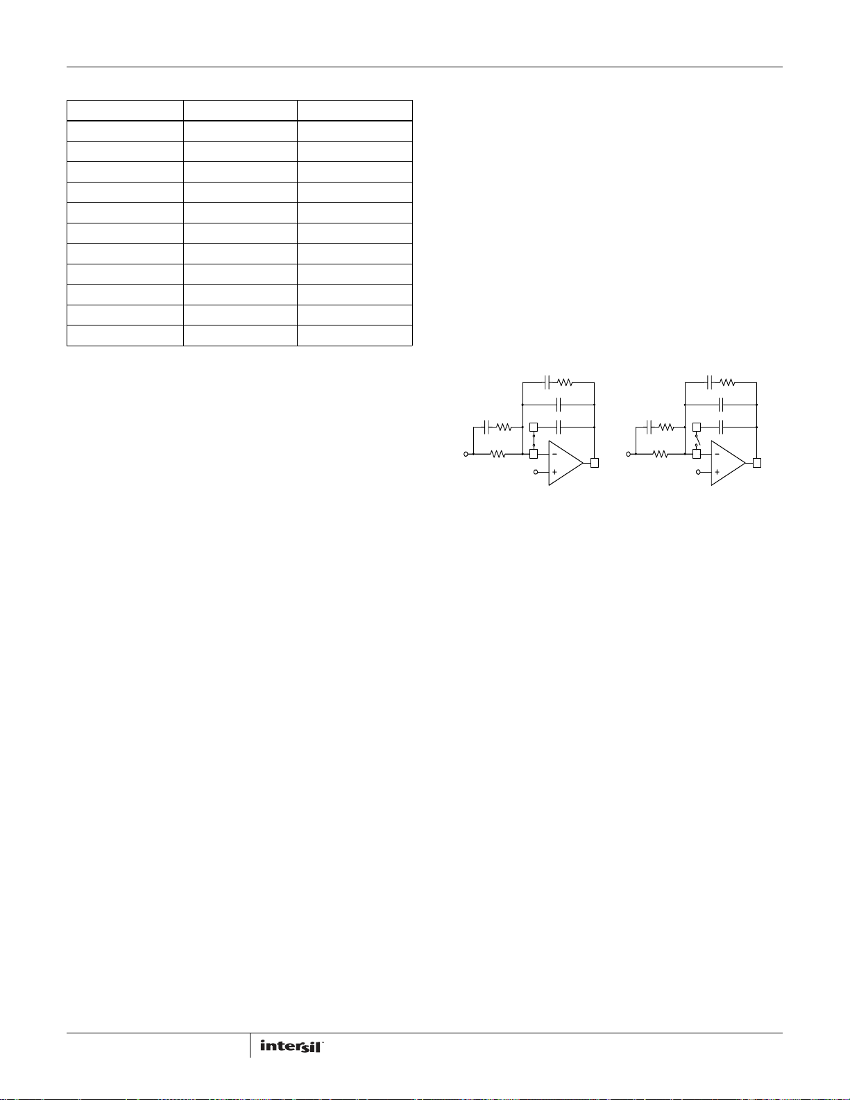
generate the Tzone value. Table 4 shows the programming table
for Tzone. The user needs to scale the NTC and the NTCG network
resistance such that it generates the NTC (and NTCG) pin voltage
that corresponds to the left-most column. Do not use any
capacitor to filter the voltage.
3% Hysteris
10
11
12
13
14
1111 1111
0111 1111
0011 1111
0001 1111
15
GerReg
Status1
16
21
FN7613.0
January 21, 2011
Page 22
ISL95831
TABLE 4. TZONE TABLE
VNTC (V) TMAX (%) TZONE
0.84 >100 FFh
0.88 100 FFh
0.92 97 7Fh
0.96 94 3Fh
1.00 91 1Fh
1.04 88 0Fh
1.08 85 07h
1.12 82 03h
1.16 79 01h
1.2 76 01h
>1.2 <76 00h
Figure 14 shows the how the NTC and the NTCG network should be
designed to get correct VR_HOT#/ALERT# behavior when the
system temperature rises and falls, manifested as the NTC and the
NTCG pin voltage falls and rises. The series of events are:
1. The temperature rises so the NTC pin (or the NTCG pin)
voltage drops. Tzone value changes accordingly.
2. The temperature crosses the threshold where Tzone register
Bit 6 changes from 0 to 1.
3. The controller changes Status_1 register bit 1 from 0 to 1.
4. The controller asserts ALERT#.
5. The CPU reads Status_1 register value to know that the alert
assertion is due to Tzone register bit 6 flipping.
6. The controller clears ALEERT#.
7. The temperature continues rising.
8. The temperature crosses the threshold where Tzone register
Bit 7 changes from 0 to 1.
9. The controllers asserts VR_HOT# signal. The CPU throttles
back and the system temperature starts dropping eventually.
10. The temperature crosses the threshold where Tzone register
bit 6 changes from 1 to 0. This threshold is 1 ADC step lower
than the one when VR_HOT# gets asserted, to provide 3%
hysteresis.
11. The controllers de-asserts VR_HOT# signal.
12. The temperature crosses the threshold where Tzone register
bit 5 changes from 1 to 0. This threshold is 1 ADC step lower
than the one when ALERT# gets asserted during the
temperature rise to provide 3% hysteresis.
13. The controller changes Status_1 register bit 1 from 1 to 0.
14. The controller asserts ALERT#.
15. The CPU reads Status_1 register value to know that the alert
assertion is due to Tzone register bit 5 flipping.
16. The controller clears ALERT#.
Current Monitor
The controller provides the current monitor function for both VRs.
The IMON pin reports VR1 inductor current and the IMONG pins
reports VR2 inductor current. Since they are designed following
the same principle, the following discussion will be only based on
the IMON pin but also applies to the IMONG pin.
The IMON pin outputs a high-speed analog current source that is
3 times of the droop current flowing out of the FB pin. Thus
becoming Equation 18:
I
IMON
As Figures 1 and 2 show, a resistor R
3I
×=
droop
is connected to the
imon
(EQ. 18)
IMON pin to convert the IMON pin current to voltage. A capacitor
should be paralleled with R
to filter the voltage information.
imon
The IMON pin voltage range is 0V to 2.658V. The controller
monitors the IMON pin voltage and considers that VR1 has
reached ICCMAX when IMON pin voltage is 2.658V.
FB2 Function
The FB2 function is only available for VR1 in 2-phase
configuration.
CONTROLLER IN
2-PHASE MODE
C2
VSEN
C1
R2
C3.1
R3
R1
C3.2
FB2
E/A
FB
VREF
FIGURE 15. FB2 FUNCTION
CONTROLLER IN
VSEN
COMP
1-PHASE MODE
C2
R1
R3
FB2
FB
VREF
C1
R2
C3.1
C3.2
E/A
COMP
Figure 15 shows the FB2 function. A switch (called FB2 switch)
turns on to short the FB and the FB2 pins when the controller is in
2-phase mode. Capacitors C3.1 and C3.2 are in parallel, serving
as part of the compensator. When the controller enters 1-phase
mode, the FB2 switch turns off, removing C3.2 and leaving only
C3.1 in the compensator. The compensator gain will increase
with the removal of C3.2. By properly sizing C3.1 and C3.2, the
compensator cab be optimal for both 2-phase mode and 1-phase
mode.
When the FB2 switch is off, C3.2 is disconnected from the FB pin.
However, the controller still actively drives the FB2 pin voltage to
follow the FB pin voltage such that C3.2 voltage always follows
C3.1 voltage. When the controller turns on the FB2 switch, C3.2
will be reconnected to the compensator smoothly.
The FB2 function ensures excellent transient response in both
2-phase mode and 1-phase mode. If one decides not to use the
FB2 function, simply populate C3.1 only.
Adaptive Body Diode Conduction Time
Reduction
In DCM, the controller turns off the low-side MOSFET when the
inductor current approaches zero. During on-time of the low-side
MOSFET, phase voltage is negative and the amount is the
MOSFET r
inductor current. A phase comparator inside the controller
monitors the phase voltage during on-time of the low-side
MOSFET and compares it with a threshold to determine the
zero-crossing point of the inductor current. If the inductor current
has not reached zero when the low-side MOSFET turns off, it’ll
flow through the low-side MOSFET body diode, causing the phase
voltage drop, which is proportional to the
DS(ON)
22
FN7613.0
January 21, 2011
Page 23

ISL95831
node to have a larger voltage drop until it decays to zero. If the
inductor current has crossed zero and reversed the direction
when the low-side MOSFET turns off, it’ll flow through the
high-side MOSFET body diode, causing the phase node to have a
spike until it decays to zero. The controller continues monitoring
the phase voltage after turning off the low-side MOSFET and
adjusts the phase comparator threshold voltage accordingly in
iterative steps such that the low-side MOSFET body diode
conducts for approximately 40ns to minimize the body dioderelated loss.
Protections
VR1 and VR2 both provide overcurrent, current-balance and
overvoltage fault protections. The controller also provides overtemperature protection. The following discussion is based on VR1
and also applies to VR2.
The controller determines overcurrent protection (OCP) by
comparing the average value of the droop current I
internal current source threshold as Table 2 shows. It declares OCP
when I
is above the threshold for 120µs.
droop
For overcurrent conditions above 1.5x the OCP level, the PWM
outputs will immediately shut off and PGOOD will go low to
maximize protection. This protection is also referred to as wayovercurrent protection or fast-overcurrent protection, for shortcircuit protection.
The controller monitors the ISEN pin voltages to determine
current-balance protection. If the ISEN pin voltage difference is
greater than 9mV for 1ms, the controller will declare a fault and
latch off.
The controller takes the same actions for all of the above fault
protections: de-assertion of both PGOODs and turn-off of all the
high-side and low-side power MOSFETs. Any residual inductor
current will decay through the MOSFET body diodes.
The controller will declare an overvoltage fault and de-assert PGOOD
if the output voltage exceeds the VID set value by +200mV. The
controller will immediately declare an OV fault, de-assert PGOOD,
and turn on the low-side power MOSFETs. The low-side power
MOSFETs remain on until the output voltage is pulled down below
the VID set value when all power MOSFETs are turned off. If the
output voltage rises above the VID set value +200mV again, the
protection process is repeated. This behavior provides the
maximum amount of protection against shorted high-side power
MOSFETs while preventing output ringing below ground.
All the above fault conditions can be reset by bringing VR_ON low
or by bringing V
V
return to their high operating levels, a soft-start will occur
DD
below the POR threshold. When VR_ON and
DD
Table 5 summarizes the fault protections.
droop
with an
TABLE 5. FAULT PROTECTION SUMMARY
FAULT DURATION
BEFORE
FAULT TYPE
Overcurrent 120µs PWM tri-state,
Phase Current
Unbalance
Way-Overcurrent
(1.5xOC)
Overvoltage
+200mV
PROTECTION
1ms
Immediately
PROTECTION
ACTION
PGOOD latched low
PGOOD latched low.
Actively pulls the
output voltage to
below VID value,
then tri-state.
FAULT
RESET
VR_ON
toggle or
VDD toggle
Supported Data And Configuration Registers
The controller supports the following data and configuration
registers.
TAB LE 6 . S UPP ORT ED DATA A ND C O NF IGURATION
Index Register Name Description
00h Vendor ID Uniquely identifies the VR
01h Product ID Uniquely identifies the VR
02h Product
05h Protocol ID Identifies what revision of SVID
06h Capability Identifies the SVID VR
10h Status_1 Data register read after ALERT#
11h Status_2 Data register showing status_2
12h Temperature
1Ch Status_2_
REGISTERS
Revision
Zone
LastRead
vendor. Assigned by Intel.
product. Intersil assigns this
number.
Uniquely identifies the revision
of the VR control IC. Intersil
assigns this data.
protocol the controller supports.
capabilities and which of the
optional telemetry registers are
supported.
signal. Indicating if a VR rail has
settled, has reached VRHOT
condition or has reached ICC
max.
communication.
Data register showing
temperature zones that have
been entered.
This register contains a copy of
the Status_2 data that was last
read with the GetReg (Status_2)
command.
Default
Value
12h
1Fh
01h
81h
00h
00h
00h
00h
23
FN7613.0
January 21, 2011
Page 24
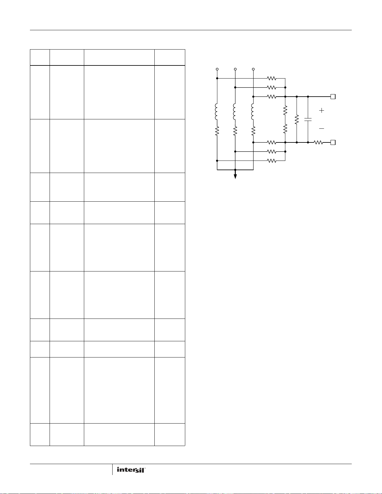
ISL95831
TAB LE 6 . S UPP ORT ED DATA A ND C ONF IGU RATI ON
REGISTERS
(Continued)
Index Register Name Description
21h ICC max Data register containing the ICC
max the platform supports, set
at start-up by resistors Rprog1
and Rprog2. The platform
design engineer programs this
value during the design process.
Binary format in amps, i.e.
100A = 64h
22h Temp max Data register containing the
temperature max the platform
support, set at startup by
resistor Rprog2. The platform
design engineer programs this
value during the design process.
Binary format in degree C, i.e.
100C = 64h
24h SR-fast Slew Rate Normal. The fastest
slew rate the platform VR can
sustain. Binary format in
mV/µs. i.e. 0Ah = 10mV/µs.
25h SR-slow Is 4x slower than normal. Binary
format in mV/µs. i.e.
02h = 2.5mV/µs
26h Vboot If programmed by the platform,
the VR supports Vboot voltage
during start-up ramp. The VR
will ramp to V
V
until it receives a new
BOOT
SetVID command to move to a
and hold at
BOOT
different voltage.
30h Vout max This register is programmed by
the master and sets the
maximum VID the VR will
support. If a higher VID code is
received, the VR will respond
with “not supported”
acknowledge.
31h VID Setting Data register containing
currently programmed VID
voltage. VID data format.
32h Power State Register containing the current
programmed power state.
33h Voltage Offset Sets offset in VID steps added to
the VID setting for voltage
margining. Bit 7 is a sign bit,
0=positive margin,
1 = negative margin.
Remaining 7 bits are # VID
steps for the margin.
00h = no margin,
01h = +1 VID step
02h = +2 VID steps...
34h Multi VR
Config
Data register that configures
multiple VRs behavior on the
same SVID bus.
Default
Value
Refer to
Tab le 7
Refer to
Tab le 8
0Ah
02h
00h
FBh
00h
00h
00h
VR1: 00h
VR2: 01h
Key Component Selection
Inductor DCR Current-Sensing Network
Phase2 Phase3
Phase1
Rsum
Rsum
Cn
Vcn
Ri
and Ro
ISUM+
ISUM-
sum
(EQ. 19)
(EQ. 20)
(EQ. 21)
(EQ. 22)
Rsum
Rntcs
Rp
Rntc
Ro
Ro
Ro
DCR
L
L
DCRLDCR
Io
FIGURE 16. DCR CURRENT-SENSING NETWORK
Figure 16 shows the inductor DCR current-sensing network for a
3-phase solution. An inductor current flows through the DCR and
creates a voltage drop. Each inductor has two resistors in R
and Ro connected to the pads to accurately sense the inductor
current by sensing the DCR voltage drop. The R
sum
resistors are connected in a summing network as shown, and feed
the total current information to the NTC network (consisting of
, R
R
ntcs
and Rp) and capacitor Cn. R
ntc
is a negative
ntc
temperature coefficient (NTC) thermistor, used to
temperature-compensate the inductor DCR change.
The inductor output side pads are electrically shorted in the
schematic, but have some parasitic impedance in actual board
layout, which is why one cannot simply short them together for the
current-sensing summing network. It is recommended to use
1Ω~10Ω Ro to create quality signals. Since Ro value is much
smaller than the rest of the current sensing circuit, the following
analysis will ignore it for simplicity.
The summed inductor current information is presented to the
capacitor C
. Equations 19 thru 23 describe the
n
frequency-domain relationship between inductor total current
(s) and Cn voltage VCn(s):
I
o
⎛⎞
R
V
Cn
R
ntcnet
A
cs
ω
L
⎜⎟
ntcnet
-----------------------------------------
s()
⎜⎟
⎜⎟
R
⎝⎠
=
----------------------
s()
=
1
DCR
----------- -
=
L
+
ntcnet
R
+()Rp×
ntcsRntc
-------------------------------------------------- -
R
++
ntcsRntcRp
s
------
1
+
ω
L
s
------------
+
ω
sns
R
sum
--------------
N
×
DCR
----------- -
N
s()× Acs× s()=
I
o
where N is the number of phases.
24
FN7613.0
January 21, 2011
Page 25
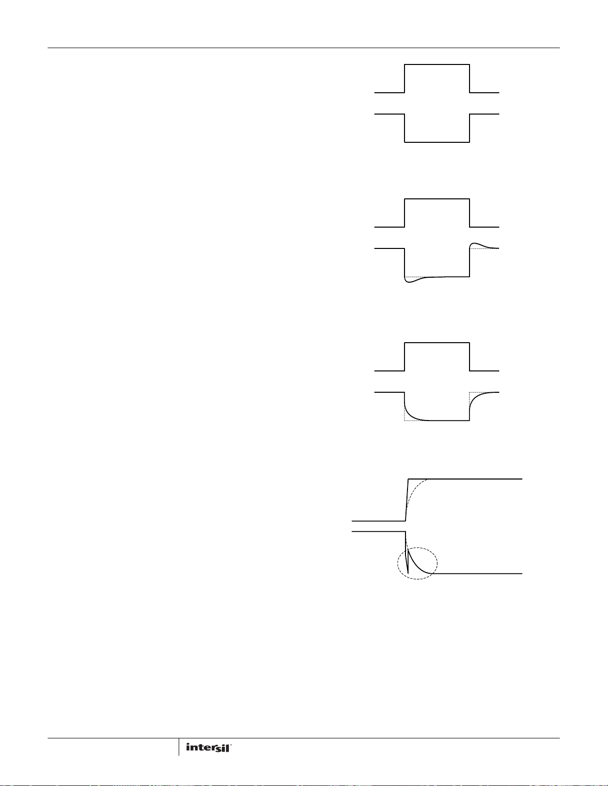
ISL95831
ntcnet
ntcnet
×
+
1
R
--------------
R
--------------
sum
N
sum
N
(EQ. 23)
×
C
n
------------------------------------------------------
ω
=
sns
R
-----------------------------------------
R
Transfer fu ncti on Acs(s) always has unity gain at DC. The inductor
DCR value increases as the winding temperature increases,
giving higher reading of the inductor DC current. The NTC R
ntc
values decrease as its temperature decreases. Proper selections
of R
sum
, Rp and R
ntcs
parameters ensure that VCn
ntc
, R
represent the inductor total DC current over the temperature
range of interest.
There are many sets of parameters that can properly temperaturecompensate the DCR change. Since the NTC network and the R
resistors form a voltage divider, V
is always a fraction of the
cn
sum
inductor DCR voltage. It is recommended to have a higher ratio of
Vcn to the inductor DCR voltage, so the droop circuit has higher
signal level to work with.
A typical set of parameters that provide good temperature
compensation are: R
and R
= 10kΩ (ERT-J1VR103J). The NTC network parameters
ntc
= 3.65kΩ, Rp= 11kΩ, R
sum
ntcs
= 2.61kΩ
may need to be fine tuned on actual boards. One can apply full
load DC current and record the output voltage reading
immediately; then record the output voltage reading again when
the board has reached the thermal steady state. A good NTC
network can limit the output voltage drift to within 2mV. It is
recommended to follow the Intersil evaluation board layout and
current-sensing network parameters to minimize engineering
time.
i
o
V
o
FIGURE 17. DESIRED LOAD TRANSIENT RESPONSE
WAVEFORMS
i
o
V
o
FIGURE 18. LOAD TRANSIENT RESPONSE WHEN Cn IS TOO
SMALL
i
o
(s) also needs to represent real-time Io(s) for the controller to
V
Cn
achieve good transient response. Transfer function Acs(s) has a
pole w
A
cs
and a zero wL. One needs to match wL and w
sns
sns
so
(s) is unity gain at all frequencies. By forcing wL equal to w
sns
and solving for the solution, Equation 24 gives Cn value.
------------------------------------------------------------
C
=
n
R
ntcnet
-----------------------------------------
R
ntcnet
For example, given N = 3, R
R
=2.61kΩ, R
ntcs
Equation 24 gives C
L
R
sum
--------------
×
N
DCR×
R
sum
--------------
+
N
= 3.65kΩ, Rp = 11kΩ,
sum
= 10kΩ, DCR = 0.9mΩ and L = 0.36µH,
ntc
= 0.397µF.
n
(EQ. 24)
Assuming the compensator design is correct, Figure 17 shows the
expected load transient response waveforms if C
selected. When the load current I
output voltage V
value is too large or too small, VCn(s) will not accurately
If C
n
represent real-time I
also has a square response.
core
(s) and will worsen the transient response.
o
has a square change, the
core
Figure 18 shows the load transient response when C
small. V
will sag excessively upon load insertion and may
core
is correctly
n
is too
n
create a system failure. Figure 19 shows the transient response
when C
is too large. V
n
is sluggish in drooping to its final
core
value. There will be excessive overshoot if load insertion occurs
during this time, which may potentially hurt the CPU reliability.
V
o
FIGURE 19. LOAD TRANSIENT RESPONSE WHEN Cn IS TOO
LARGE
i
o
i
L
V
o
RING
BACK
FIGURE 20. OUTPUT VOLTAGE RING BACK PROBLEM
25
FN7613.0
January 21, 2011
Page 26
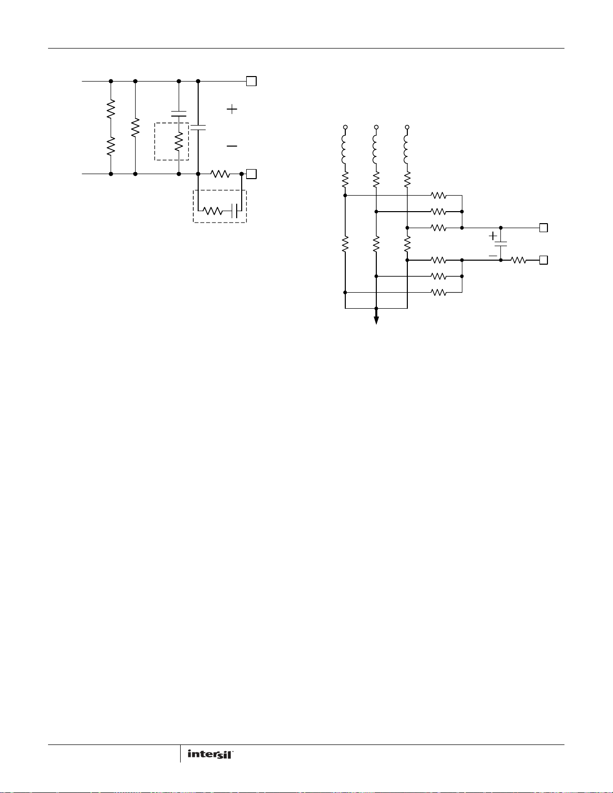
ISL95831
ISUM+
Rntcs
Rp
Rntc
FIGURE 21. OPTIONAL CIRCUITS FOR RING BACK REDUCTION
Cn.1
Rn
OPTIONAL
Vcn
Cn.2
Ri
Cip
Rip
OPTIONAL
ISUM-
Figure 20 shows the output voltage ring back problem during
load transient response. The load current io has a fast step
change, but the inductor current i
cannot accurately follow.
L
Instead, iL responds in first order system fashion due to the
nature of current loop. The ESR and ESL effect of the output
capacitors makes the output voltage V
dip quickly upon load
o
current change. However, the controller regulates Vo according to
the droop current i
therefore it pulls V
, which is a real-time representation of iL;
droop
back to the level dictated by iL, causing the
o
ring back problem. This phenomenon is not observed when the
output capacitor have very low ESR and ESL, such as all ceramic
capacitors.
Figure 21 shows two optional circuits for reduction of the ring
back.
is the capacitor used to match the inductor time constant. It
C
n
usually takes the parallel of two (or more) capacitors to get the
desired value. Figure 21 shows that two capacitors C
are in parallel. Resistor R
the Vo ring back. At steady state, C
capacitance. At the beginning of io change, the effective
C
n
capacitance is less because R
branch. As Figure 18 explains, Vo tends to dip when Cn is too
C
n.1
small, and this effect will reduce the V
more pronounced when C
more pronounced when R
increases the ripple of the Vn signal if C
R
n
recommended to keep C
usually is a few ohms. C
is an optional component to reduce
n
is much larger than C
n.1
is bigger. However, the presence of
n
greater than 2200pF. Rn value
n.2
, C
n.1
n.2
+ C
n.1
increases the impedance of the
n
provides the desired
n.2
ring back. This effect is
o
is too small. It is
n.2
and Rn values should be
n.1
. It is also
n.2
and C
n.2
determined through tuning the load transient response
waveforms on an actual board.
and Cip form an R-C branch in parallel with Ri, providing a
R
ip
lower impedance path than R
and C
do not have any effect at steady state. Through proper
ip
selection of Rip and Cip values, i
, and Vo will not ring back. The recommended value for Rip is
i
L
100Ω. C
should be determined through tuning the load
ip
at the beginning of io change. Rip
i
can resemble io rather than
droop
transient response waveforms on an actual board. The
recommended range for C
should be noted that the R
is 100pF~2000pF. However, it
ip
-Cip branch may distort the i
ip
droop
waveform. Instead of being triangular as the real inductor
current, i
affect i
may have sharp spikes, which may adversely
droop
average value detection and therefore may affect
droop
OCP accuracy. User discretion is advised.
Resistor Current-Sensing Network
Phase1
DCR
Rsen
Figure 22 shows the resistor current-sensing network for a
2-phase solution. Each inductor has a series current-sensing
resistor R
accurately capture the inductor current information. The R
and R
form a a filter for noise attenuation. Equations 25 thru 27 give
VCn(s) expression:
VCns()
A
Rsen
ω
Rsen
Transfer function A
Current-sensing resistor R
variation over-temperature, so there is no need for the NTC
network.
The recommended values are R
Phase2 Phase3
L
DCRLDCR
Rsen Rsen
Io
FIGURE 22. RESISTOR CURRENT-SENSING NETWORK
. R
sen
resistors are connected to capacitor Cn. R
o
R
sen
------------
N
-------------------------- -
s()
=
1
1
---------------------------
=
R
sum
--------------
N
L
Rsum
Rsum
Rsum
Ro
Ro
Ro
and Ro are connected to the R
sum
s()× A
× s()=
I
o
Rsen
1
s
----------------
+
ω
Rsen
×
C
n
(s) always has unity gain at DC.
Rsen
value will not have significant
sen
= 1kΩ and Cn= 5600pF.
sum
Vcn
Cn
Ri
sen
sum
Overcurrent Protection
Refer to Equation 1 on page 18 and Figures 16, 20 and 22;
resistor Ri sets the droop current I
internal OCP threshold. It is recommended to design I
without using the R
comp
resistor.
For example, the OCP threshold is 60µA for 3-phase solution. We
will design I
to be 40.9µA at full load, so the OCP trip level is
droop
1.5x of the full load current.
For inductor DCR sensing, Equation 28 gives the DC relationship
(s) and Io(s).
of V
cn
. Tables 2 and 3 show the
droop
ISUM+
ISUM-
pads to
sum
and Cn
(EQ. 25)
(EQ. 26)
(EQ. 27)
droop
26
FN7613.0
January 21, 2011
Page 27
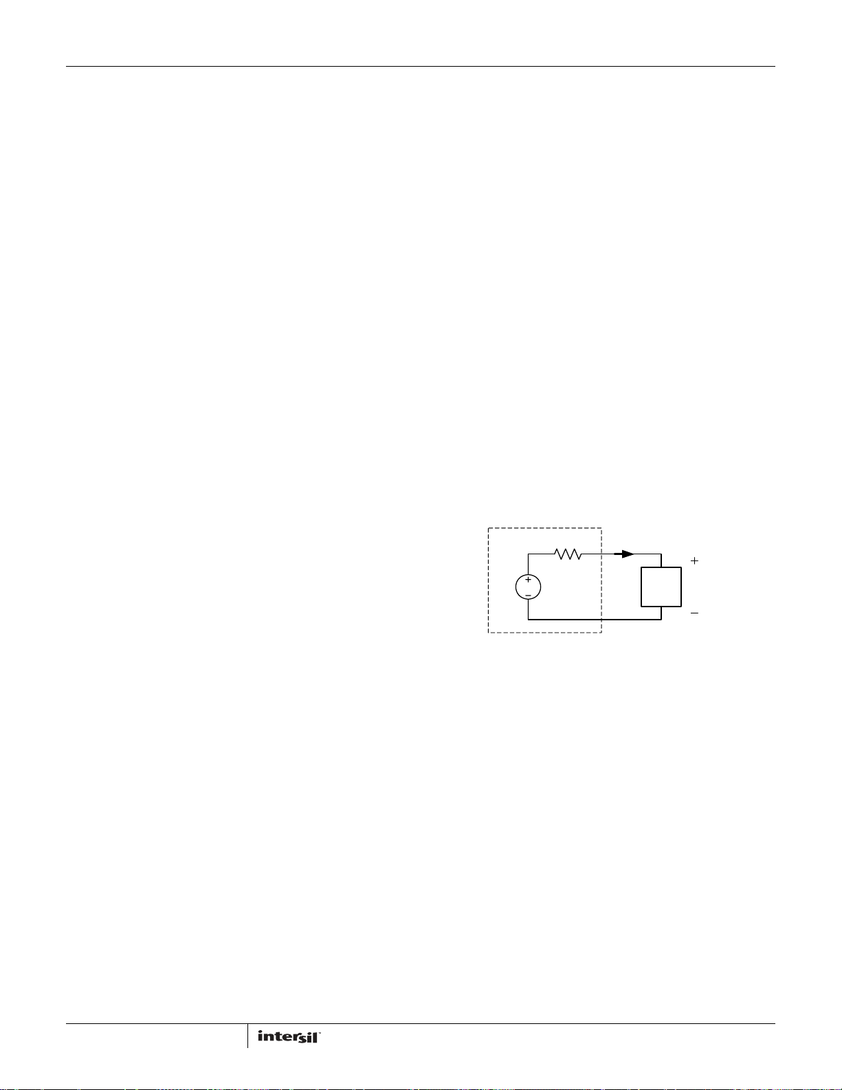
ISL95831
⎛⎞
R
⎜⎟
ntcnet
-----------------------------------------
V
⎜⎟
Cn
⎜⎟
R
ntcnet
+
⎝⎠
R
sum
--------------
N
×
DCR
----------- -
N
×=
I
o
(EQ. 28)
Substitution of Equation 28 into Equation 1 gives Equation 29:
I
droop
2
---- -
-----------------------------------------
R
i
R
ntcnet
R
ntcnet
+
R
sum
--------------
N
DCR
----------- -
×=
×× I
N
o
(EQ. 29)
Therefore:
2R
ntcnet
------------------------------------------------------------------------------- -
R
=
i
⎛⎞
NR
× I
ntcnet
⎝⎠
+
DCR× Io×
R
sum
--------------
N
×
(EQ. 30)
droop
Substitution of Equation 20 and application of the OCP condition
in Equation 30 gives Equation 31:
R
+()Rp×
ntcsRntc
-------------------------------------------------- -
2
× DCR× I
R
++
-------------------------------------------------------------------------------------------------------------------------
R
=
i
N
where I
ntcsRntcRp
R
+()Rp×
⎛⎞
ntcsRntc
-------------------------------------------------- -
× I
⎜⎟
R
++
⎝⎠
ntcsRntcRp
is the full load current, I
omax
+
R
sum
--------------
N
×
omax
×
droopmax
droopmax
(EQ. 31)
is the
corresponding droop current. For example, given N = 3,
= 3.65kΩ, Rp = 11kΩ, R
R
sum
DCR = 0.9mΩ, I
omax
= 94A and I
= 2.61kΩ, R
ntcs
droopmax
= 10kΩ,
ntc
= 48µA, Equation 31
gives Ri = 974Ω.
For resistor sensing, Equation 32 gives the DC relationship of
V
(s) and Io(s).
cn
R
sen
------------
V
Cn
×=
I
o
N
(EQ. 32)
Substitution of Equation 32 into Equation 1 gives Equation 33:
R
2
sen
---- -
I
droop
------------
××=
I
o
N
R
i
(EQ. 33)
Therefore:
2R
×
R
i
senIo
---------------------------
=
×
NI
droop
(EQ. 34)
Substitution of Equation 34 and application of the OCP condition
in Equation 30 gives Equation 35:
2R
×
senIomax
--------------------------------------
R
=
i
where I
NI
×
droopmax
is the full load current, I
omax
droopmax
is the
(EQ. 35)
corresponding droop current. For example, given N = 3,
R
sen
gives R
=1mΩ, I
= 1305Ω.
i
omax
= 94A and I
droopmax
= 48µA, Equation 35
Load Line Slope
Refer to Figure 9.
For inductor DCR sensing, substitution of Equation 29 into
Equation 2 gives the load line slope expression:
LL
V
droop
----------------- -
I
o
2R
droop
----------------------
R
i
R
ntcnet
-----------------------------------------
R
ntcnet
+
R
sum
--------------
N
DCR
----------- -
××== (EQ. 36)
N
For resistor sensing, substitution of Equation 33 into Equation 2
gives the load line slope expression:
V
droop
----------------- -
LL
==
I
o
2R
×
senRdroop
-----------------------------------------
NR
×
i
(EQ. 37)
Substitution of Equation 30 and rewriting Equation 36, or
substitution of Equation 34 and rewriting Equation 37 give the
same result in Equation 38:
I
o
R
droop
----------------
I
One can use the full load condition to calculate R
example, given I
Equation 38 gives R
It is recommended to start with the R
droop
LL×=
omax
= 94A, I
droop
droopmax
= 3.72kΩ.
(EQ. 38)
. For
droop
= 48µA and LL = 1.9mΩ,
value calculated by
droop
Equation 38, and fine tune it on the actual board to get accurate
load line slope. One should record the output voltage readings at
no load and at full load for load line slope calculation. Reading
the output voltage at lighter load instead of full load will increase
the measurement error.
Compensator
Figure 17 shows the desired load transient response waveforms.
Figure 23 shows the equivalent circuit of a voltage regulator (VR)
with the droop function. A VR is equivalent to a voltage source
(= VID) and output impedance Z
out
(s). If Z
load line slope LL, i.e. constant output impedance, in the entire
frequency range, Vo will have square response when Io has a
square change.
VR
i
o
Z
(s) = LL
out
VID
FIGURE 23. VOLTAGE REGULATOR EQUIVALENT CIRCUIT
Intersil provides a Microsoft Excel-based spreadsheet to help
design the compensator and the current sensing network, so the
VR achieves constant output impedance as a stable system.
Please go to www.intersil.com/design/ to request spreadsheet.
Figure 26
shows a screenshot of the spreadsheet.
A VR with active droop function is a dual-loop system consisting of
a voltage loop and a droop loop which is a current loop. However,
neither loop alone is sufficient to describe the entire system. The
spreadsheet shows two loop gain transfer functions, T1(s) and
T2(s), that describe the entire system. Figure 24 conceptually
shows T1(s) measurement set-up and Figure 25 conceptually
shows T2(s) measurement set-up. The VR senses the inductor
current, multiplies it by a gain of the load line slope, then adds it
on top of the sensed output voltage and feeds it to the
compensator. T(1) is measured after the summing node, and T2(s)
is measured in the voltage loop before the summing node. The
spreadsheet gives both T1(s) and T2(s) plots. However, only T2(s)
can be actually measured on an ISL95831 regulator.
(s) is equal to the
out
LOAD
V
o
27
FN7613.0
January 21, 2011
Page 28
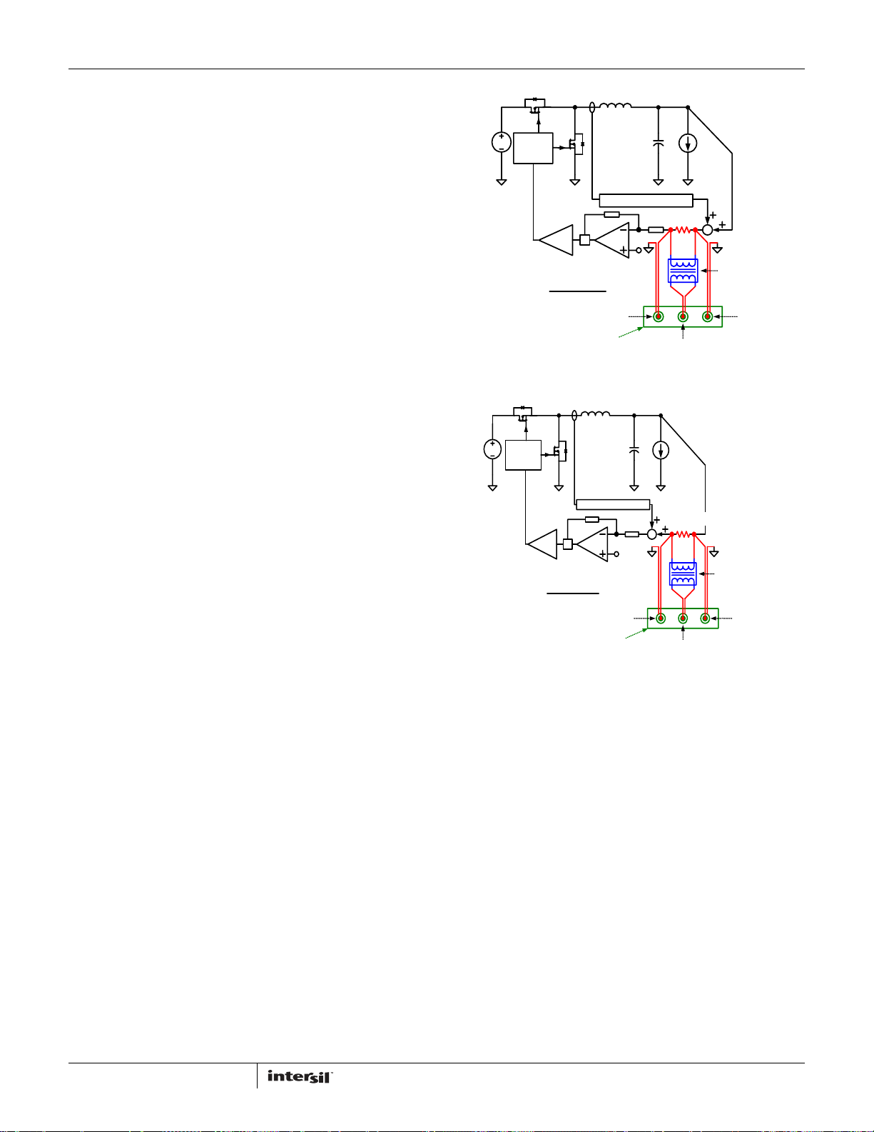
ISL95831
T1(s) is the total loop gain of the voltage loop and the droop loop.
It always has a higher crossover frequency than T2(s) and has
more meaning of system stability.
T2(s) is the voltage loop gain with closed droop loop. It has more
meaning of output voltage response.
Design the compensator to get stable T1(s) and T2(s) with
sufficient phase margin, and output impedance equal or smaller
than the load line slope.
out
V
20
o
i
o
Ω
Q1
V
GATE
in
DRIVER
LOOP GAIN =
Q2
MOD.
COMP
CHANNEL B
CHANNEL A
NETWORK
ANALYZER
L
C
LOAD LINE SLOPE
EA
VID
EXCITATION OU T P UT
FIGURE 24. LOOP GAIN T1(s) MEASUREMENT SET-UP
V
O
OUT
VID
EXCITATION OUTPUT
I
O
Ω
20
Q1
V
IN
LOOP GAIN =
GATE
DRIVER
Q2
MOD.
COMP
CHANNEL B
CHANNEL A
L
C
LOAD LINE SLOPE
EA
NETWORK
ANALYZER
ISOLATION
TRANSFORMER
CHANNEL BCHANNEL A
ISOLAT ION
TRANSFORMER
CHANNEL BCHANNEL A
28
FIGURE 25. LOOP GAIN T2(s) MEASUREMENT SET-UP
January 21, 2011
FN7613.0
Page 29
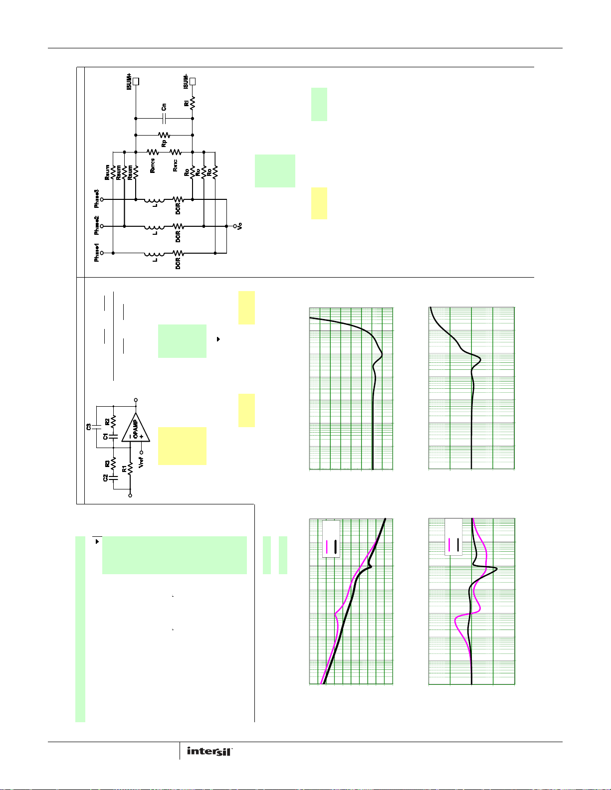
ISL95831
Vi
lt
·
§
·
V
:
:
:
pp
:
:
:
Desired Load
Line Slope:
:
Performance and Stability
Desired
Load
Line
Slope:
9
:
Performance
and
Stability
O t t I d Z(f) G i C
:
*DLQG%
D
JQLWXGHPRKP
*DLQG%
)UHTXHQF\+]
0DJQLWXGHPRKP
)UHTXHQF\+]
Loop Gain Phase Curve
*DLQG%
)UHTXHQF\+]
0DJQLWXGHPRKP
)UHTXHQF\+]
KDVHGHJUHH
3
KDVHGHJUHH
*DLQG%
)UHTXHQF\+]
0DJQLWXGHPRKP
)UHTXHQF\+]
3KDVHGHJUHH
)UHTXHQF\+]
3KDVHGHJUHH
)UHTXHQF\+]
k
m
k
k
k
Operation Parameters
Ri 974
¸¸¹
·
¸¸¹
·
¸¸¹
·
¸¸¹
·
¸¸¹
·
¸¸¹
·
¸¸¹
·
¸¸¹
·
21
21
21
21
21
21
21
21
zz
zz
zz
zz
zz
zz
zz
zz
f
f
f
f
f
f
f
f
¸¸¹
·
¸¸¹
·
¸¸¹
·
¸¸¹
·
¸¸¹
·
¸¸¹
·
¸¸¹
·
s
s
s
s
s
s
s
s
SS
SS
SS
SS
SS
SS
SS
SS
21
21
21
21
21
21
21
pp
pp
pp
pp
pp
pp
pp
2
2
2
2
2
2
2
2
f
f
f
f
f
f
f
s
s
s
s
s
s
s
SS
SS
SS
SS
SS
SS
SS
2
2
2
2
2
2
2
1
1
1
1
1
1
1
1
¨¨©
§
¨¨©
§
¨¨©
§
¨¨©
§
¨¨©
§
¨¨©
§
¨¨©
§
¨¨©
§
¸¸¹
·
¸¸¹
·
¸¸¹
·
¸¸¹
·
¸¸¹
·
¸¸¹
·
¸¸¹
·
¸¸¹
·
1
1
1
1
1
1
1
¨¨©
§
¨¨©
§
¨¨©
§
¨¨©
§
¨¨©
§
¨¨©
§
¨¨©
§
f
f
f
f
f
f
f
f
s
s
s
s
s
s
s
s
¸¸¹
·
¸¸¹
·
¸¸¹
·
¸¸¹
·
¸¸¹
·
¸¸¹
·
¸¸¹
·
2
2
2
2
2
2
2
2
f
f
f
f
f
f
f
s
s
s
s
s
s
s
1
1
1
1
1
1
1
1
2
2
2
2
2
2
2
¨¨©
§
¨¨©
§
¨¨©
§
¨¨©
§
¨¨©
§
¨¨©
§
¨¨©
§
¨¨©
§
i
i
i
i
i
i
i
i
1
1
1
1
1
1
1
ZZ
ZZ
ZZ
ZZ
ZZ
ZZ
ZZ
ZZ
¨¨©
§
¨¨©
§
¨¨©
§
¨¨©
§
¨¨©
§
¨¨©
§
¨¨©
§
iK
iK
iK
iK
iK
iK
iK
iK
s
s
s
s
s
s
s
)(
)(
)(
)(
)(
)(
)(
)(
sA
sA
sA
sA
sA
sA
sA
sA
V
V
V
V
V
V
V
k
R1 3.74
k
k
R2 200
k
k
R3 0.499
k
Compensator Parameters Current Sensing Network Parameters
R1 3.721
Recommended Value User-Selected Value
Inductor DCR 0.9
N
N
N
N
N
N
Use User-Selected Value (Y/N)?
C2 582.215 pF C2 470 pF
Ri 973.415
Cn 0.397 uF Cn 0.397 uF
Recommended Value User Selected Value
Output Impedance Z(f), Gain Curve
Output Impedance Z(f), Gain Curve
Output Impedance Z(f), Gain Curve
Output Impedance Z(f), Gain Curve
Output Impedance Z(f), Phase Curve
Output Impedance Z(f), Phase Curve
( ( ( ( ( ( ( (
( ( ( ( ( ( ( (
( ( ( ( ( ( ( (
( ( ( ( ( ( ( (
Compensation & Current Sensing Network Design for Intersil Multiphase R^3 Regulators.
ISL9583x
ISL9583x
ISL9583x
ISL9583x
ISL9583x
ISL9583x
ISL9583x
ISL9583x
Vin: 12 volts
Vo: 1 volts
m
m
m
.
xfs (Switching Frequency)
1.3 Rntcs 2.61
7V
7V
7V
7V
7V
7V
7V
7V
-
-
Phase Number: 3
Operation Parameters
Full Load Current: 94 Amps
Controller Part Number:
Switching Frequency: 300 kHz
Inductance Per Phase: 0.36 uH
CPU Socket Resistance: 0.9
Loop Gain, Gain Curve
Loop Gain, Gain Curve
Loop Gain, Gain Curve
Loop Gain, Gain Curve
Estimated Full-Load Efficiency: 84 %
Number of Output Bulk Capacitors: 4
ESL of Each Output Bulk Capacitor: 0.2 nH R2 239.499
ESR of Each Output Bulk Capacitor: 4.5
Number of Output Ceramic Capacitors: 28 R3 0.607
ESL of Each Output Ceramic Capacitor: 3 nH C3 49.112 pF C3 47 pF
ESR of Each Output Ceramic Capacitor: 3
Capacitance of Each Output Bulk Capacitor: 560 uF
Revision 8.3
Attention: 1. "Analysis ToolPak" Add-in is required. To turn on, go to Tools--Add-Ins, and check "Analysis ToolPak"
2. Green cells require user input
Capacitance of Each Output Ceramic Capacitor: 10 uF C1 478.156 pF C1 150 pF
Desired Idroop Current at Full Load: 48 uA T1 Bandwidth: 182kHz T2 Bandwidth: 33kHz
(This sets the over-current protection level) T1 Phase Margin: 71.° T2 Phase Margin: 96.8°
Changing the settings in red requires deep understanding of control loop design
Place the 2nd compensator pole fp2 at: 1.5 Rsum 3.65
(Recommended Ki range is 0.8~2) Rp 11
Tune the compensator gain factor Ki:
Tune Ki to get the desired loop gain bandwidth Rntc 10
( ( ( ( ( ( ( (
( ( ( ( ( ( ( (
( ( ( ( ( ( ( (
29
7V
7V
7V
7V
Loop Gain, Phase Curve
Loop Gain, Phase Curve
January 21, 2011
FIGURE 26. SCREENSHOT OF THE COMPENSATOR DESIGN SPREADSHEET
( ( ( ( ( ( ( (
FN7613.0
Page 30
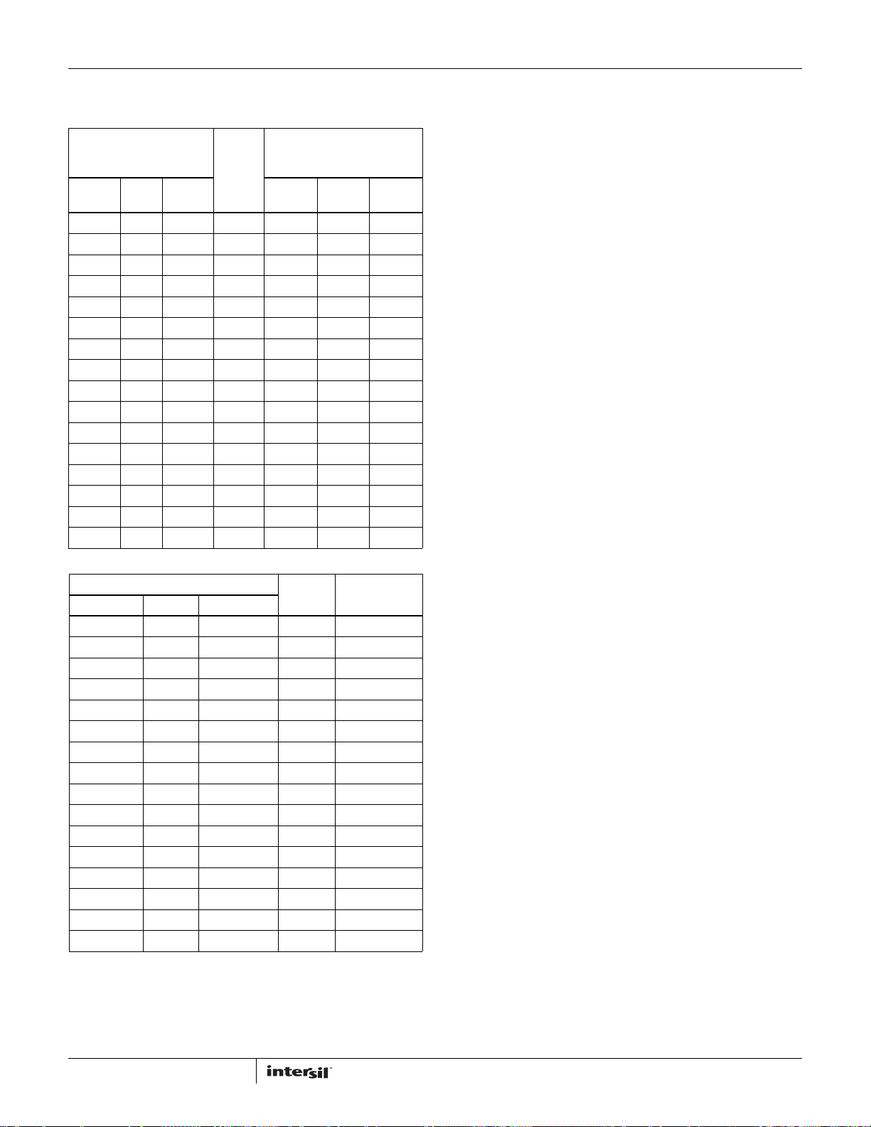
ISL95831
Programming Resistors
TABLE 7. RPROG1 PROGRAMMING TABLE
VR1 ICCMAX (A)
RPROG1
(kohm)
Min.
(-3%) Typ.
0.57 0.59 0.61 0 93 62 31
1.07 1.1 1.13 0 87 58 29
1.64 1.69 1.74 0 81 54 27
2.19 2.26 2.33 0 75 50 25
3.07 3.16 3.25 0 69 46 23
4.19 4.32 4.45 0 63 42 21
5.33 5.49 5.65 0 57 38 19
6.45 6.65 6.85 1.1 57 38 19
7.63 7.87 8.11 1.1 63 42 21
9.03 9.31 9.59 1.1 69 46 23
11.16 11.5 11.85 1.1 75 50 25
13.29 13.7 14.11 1.1 81 54 27
15.71 16.2 16.69 1.1 87 58 29
18.14 18.7 19.26 1.1 93 62 31
24.15 24.9 open 1.1 99 66 33
0.57 0.59 0.61 120 29
1.07 1.1 1.13 120 25
1.64 1.69 1.74 120 21
2.19 2.26 2.33 110 21
3.07 3.16 3.25 110 25
4.19 4.32 4.45 110 29
5.33 5.49 5.65 110 33
6.45 6.65 6.85 105 33
7.63 7.87 8.11 105 29
9.03 9.31 9.59 105 25
11.16 11.5 11.85 105 21
13.29 13.7 14.11 95 21
15.71 16.2 16.69 95 25
18.14 18.7 19.26 95 29
24.15 24.9 open 95 33
Max.
(+3%) 3-PH 2-PH 1-PH
0 0 99 66 33
TABLE 8. RPROG2 PROGRAMMING TABLE
RPROG2 (kΩ)
0 120 33
V
BOOT
(V)
With POWER-UP
CONFIGURATION
TMAX (°C) VR2 ICCMAX (A)Min.(-3%) Typ. Max.(+3%)
register settings. VR1 can power to 0V V
V
based on R
BOOT
actual CPU, select R
value. When the controller works with an
prog1
such that VR1 powe rs up to V
prog1
or an internally-set
BOOT
BOOT
= 0V
as required by the SVID command. In the absence of a CPU, such
as testing of the VR alone, select R
up to the internally-set V
, which by default is 1.1V.
BOOT
such that VR1 powers
prog1
Determine the maximum current VR1 can support and set the
VR1 ICCMAX register value accordingly by selecting the
appropriate R
value. The CPU will read the VR1 ICCMAX
prog1
register value and ensure that the CPU CORE current doesn’t
exceed the value specified by VR1 ICCMAX.
Table 8 shows how to select R
ICCMAX register settings. There are four T
prog2
based on T
MAX
and VR2
MAX
temperatures to
choose from: +120°C, +110°C, +105°C, and +95°C. There are
also four VR2 ICCMAX values to choose from:
Current Monitor
Refer to Equation 18 for the IMON pin current expression.
Referring to Figures 1 and 2 on page 6 and page 7, the IMON pin
current flows through R
. The voltage across R
imon
imon
is
expressed in Equation 39:
V
Rimon
3I×
droopRimon
×=
(EQ. 39)
Rewriting Equation 38 gives Equation 40:
I
o
I
droop
------------------
R
droop
LL×=
(EQ. 40)
Substitution of Equation 40 into Equation 39 gives Equation 41:
3IoLL×
V
Rimon
---------------------
R
droop
×=
R
imon
(EQ. 41)
Rewriting Equation 41 and application of full load condition gives
Equation 42:
V
×
RimonRdroop
imon
=
= 18.6kΩ.
--------------------------------------------
3I
LL×
o
= 2.658V at I
can be paralleled with R
imon
imonCimon
= 3.74kΩ,
droop
=94A, Equation 42 gives
omax
to filter the IMON
imon
time constant is the user’s choice. It
(EQ. 42)
R
For example, given LL = 1.9mΩ, R
V
Rimon
R
imon
A capacitor C
pin voltage. The R
is recommended to have a time constant long enough such that
switching frequency ripples are removed.
Current Balancing
Refer to Figures 1 thru 2. The controller achieves current
balancing through matching the ISEN pin voltages. R
C
form filters to remove the switching ripple of the phase
isen
node voltages. It is recommended to use rather long R
time constant such that the ISEN voltages have minimal ripple
and represent the DC current flowing through the inductors.
Recommended values are R
= 10kΩ and Cs= 0.22µF.
s
and
isen
isenCisen
There are two programming resistors: R
shows how to select R
prog1
based on V
30
and R
prog1
and VR1 ICCMAX
BOOT
prog2
. Table 7
FN7613.0
January 21, 2011
Page 31
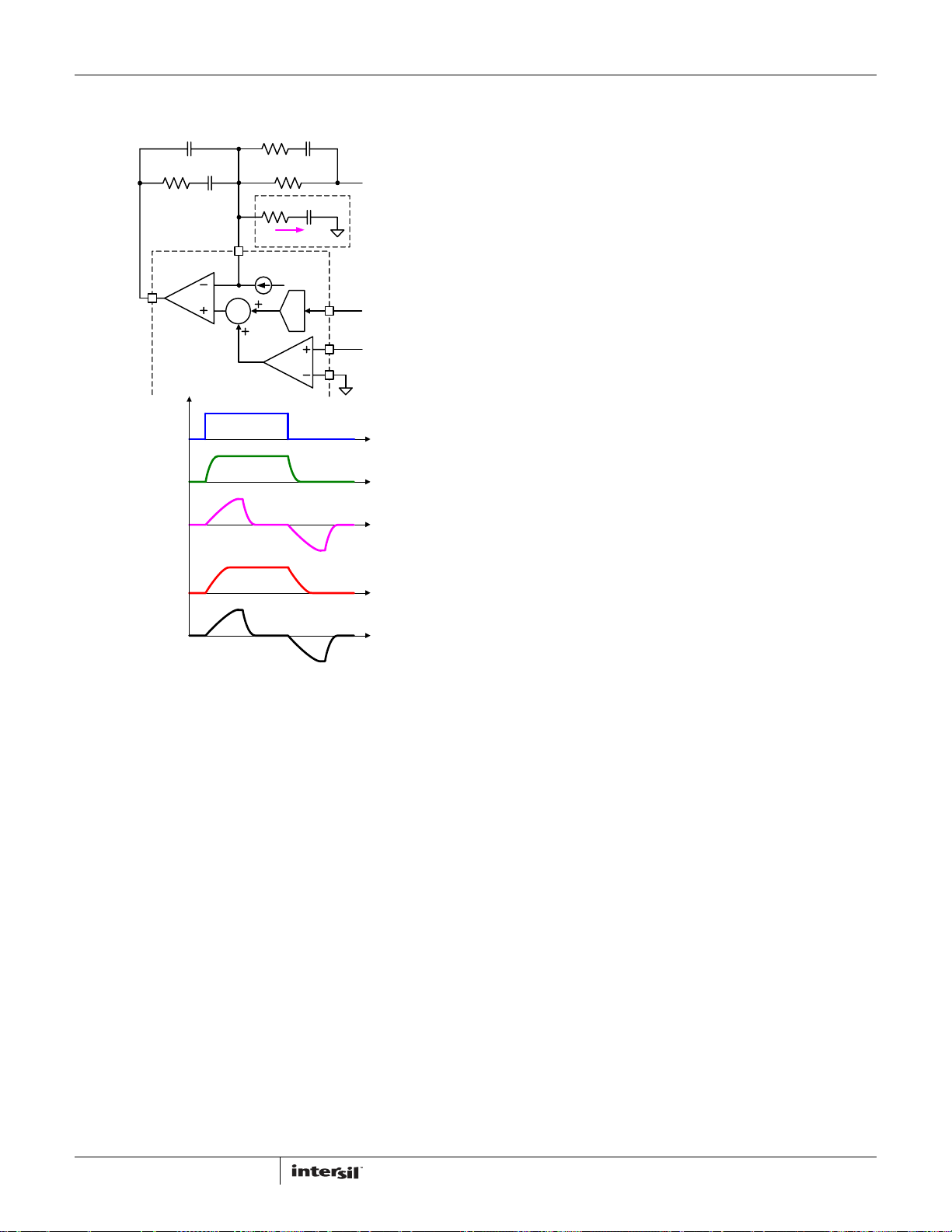
ISL95831
Slew Rate Compensation Circuit For VID
Transition
COMP
E/A
INTERNAL TO
IC
VID
Vfb
Ivid
FB
Idroop_vid
Σ
Rdroop
Rvid
VDAC
Cvid
Ivid
DAC
X 1
OPTIONAL
VIDs
RTN
VSS
Vcore
VID
VSSSENSE
During a large VID transition, the DAC steps through the VIDs at a
controlled slew rate. For example, the DAC may change a tick
(5mV) per 0.5µs, controlling output voltage V
slew rate at
core
10mV/µs.
Figure 27 shows the waveforms of VID transition. During VID
transition, the output capacitor is being charged and discharged,
causing C
out
x dV
/dt current on the inductor. The controller
core
senses the inductor current increase during the up transition, as
the I
droop_vid
V
accordingly, making V
core
occurs during the down transition. To get the correct V
rate during VID transition, one can add the R
whose current I
waveform shows, and will droop the output voltage
slew rate slow. Similar behavior
cancels I
vid
core
droop_vid
.
vid-Cvid
slew
core
branch,
It’s recommended to choose the R, C values from the reference
design as a starting point. then tweak the actual values on the
board to get the best performance.
During normal transient response, the FB pin voltage is held
constant, therefore is virtual ground in small signal sense. The R
- C
network is between the virtual ground and the real ground,
vid
vid
and hence has no effect on transient response.
Vcore
Idroop_vid
FIGURE 27. SLEW RATE COMPENSATION CIRCUIT FOR VID
TRANSITION
31
FN7613.0
January 21, 2011
Page 32
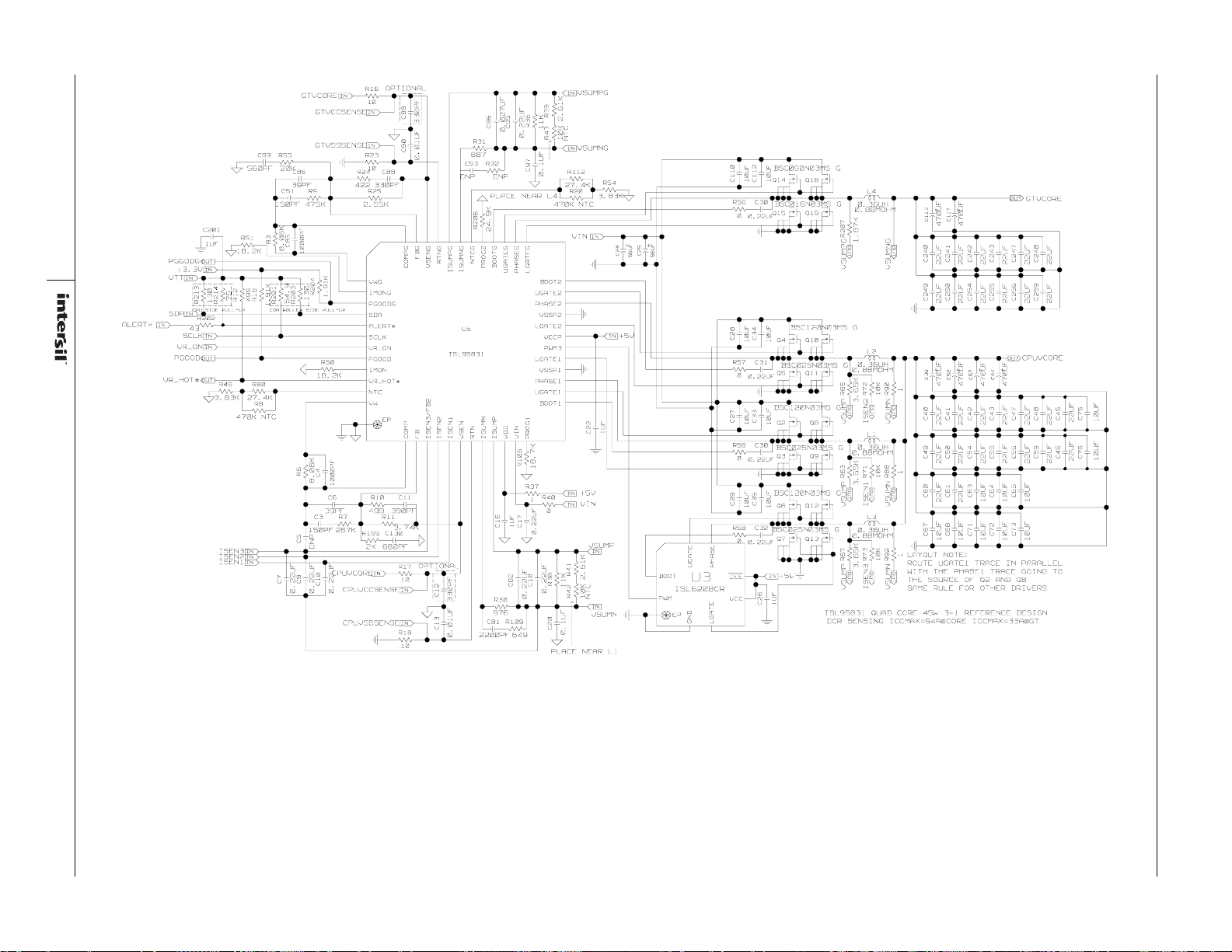
32
A
LERT#
OPTIONAL
R16
R24
R155
10
IN
IN
R23
10
330PF
R25
2.55K
VWG
IMONG
PGOODG
SDA
ALERT#
SCLK
VR_ON
PGOOD
IMON
VR_HOT#
NTC
VW
R10
499
2K
IN
C88
EP
390PF
R11
3.74K
C130
680PF
----
C89
-----
----
C90
COMPG
COMP
C11
R17
10
IN
IN
R18
10
-----
330PF
0.01UF
FBG
RTNG
VSENG
ISL95831
ISEN3/FB2
ISEN2
FB
OPTIONAL
----
C12
-----
----
C13
887
C93
DNP
ISUMPG
ISUMNG
U6
ISEN1
VSEN
-----
0.01UF 330PF
C95
C96
0.027UF
R31
R32
DNP
PLACE NEAR L4
R206
24.9K
NTCG
PROG2
BOOTG
UGATEG
ISUMP
ISUMN
RTN
VDD
C16
R30
976
R109
C81
2200PF
649
IN
GTVCORE
GTVCCSENSE
R55
20K
C51
150PF
R3
R201
1.91K
----
C7
C86
39PF
C85
8.06K
54.9
R203
R6
C5
C9
0.22UF
GTVSSSENSE
R9
475K
1000PF
R204
1.91K
130
----
R50
18.2K
C4
8.06K
C6
39PF
C3
150PF
DNP
CPUVCORE
C10
0.22UF
422
1000PF
R7
267K
CPUVCCSENSE
0.22UF
C99
560PF
C201
R51
1UF
18.2K
OUT
PGGODG
IN
+3.3V
IN
VTT
--------
130
R214
R213
----
--------
CPU SIDE PULL-UP
IN
SDA
R202
IN
43
IN IN
SCLK
IN
VR_ON
OUT
PGOOD
OUT
VR_HOT#
R49
3.83K
ISEN3
ISEN2
ISEN1
75
R12
----
470K
499
R80
27.4K
R8
IN
IN
IN
--------
R19
--------
CONTROLLER SIDE PULL-UP
NTC
CPUVSSSENSE
FIGURE 28. ISL95831 3+1 45W REFERENCE DESIGN
0.22UF
PHASEG
VIN
R106
R37
1UF
C17
C82
R36
C97
LGATEG
PROG1
1
0.22UF
IN
R39
2.61K
11K
R43
10K
NTC
IN
---->
R112
0.1UF
27.4K
R20
470K
BOOT2
UGATE2
PHASE2
VSSP2
LGATE2
VCCP
PWM3
LGATE1
VSSP1
PHASE1
UGATE1
BOOT1
18.7K
IN
R40
IN
0
0.22UF
R38
C18
11K
0.22UF
C20
0.1UF
PLACE NEAR L1
VSUMPG
VSUMNG
R54
3.83K
NTC
IN
VIN
C22
+5V
VIN
VSUMP
IN
R41
2.61K
R42
10K
NTC
IN
VSUMN
---------->
1UF
C24
+5V
56UF
C25
56UF
BOOT
ISL6208CR
PWM
EP
UGATE
U3
GND
PHASE
LGATE
C110
0
C28
R57
0
C27
R56
0
C29
R58
0
DEE
VCC
BSC090N03MS G
10UF
10UF
C112
Q14
C30R56
BSC016N03MS G
Q15
0.22UF
C34
10UF
10UF
C31
0.22UF
BSC120N03MS G
C33
10UFQ210UF
C30
BSC025N03MS G
0.22UF
BSC120N03MS G
C35
10UF
10UF
C32
BSC025N03MS G
0.22UF
IN
C26
Q18
Q19
BSC120N03MS G
Q10
Q4
BSC025N03MS G
Q5
Q11
Q8
Q3
Q9
Q6
Q12
Q13
Q7
+5V
1UF
ISL95831 QUAD CORE 45W 3+1 REFERENCE DESIGN
DCR SENSING ICCMAX=94A@CORE ICCMAX=33A@GT
L4
0.36UH
0.88MOHM
R207
1.87K
OUT
VSUMPG
L2
0.36UH
0.88MOHM
R72R71
R65
3.65K
OUT OUT
OUT
ISEN2
VSUMP
L1
0.36UH
0.88MOHM
R63
3.65K3.65K
OUT
ISEN1
VSUMP
L3
0.36UH
0.88MOHM
R73
R67
OUT
OUT
ISEN3
VSUMP
C117
C113
470UF
470UF
OUT
C241
C240
VSUMNG
10K
R90
VSUMN
10K
R88
OUT
VSUMN
10K
R92
OUTOUT
VSUMN
22UF
C249
22UF
C39
1
C40
22UF 470UF
C49
22UF
1
C60
22UF
C67
10UF
1
LAYOUT NOTE:
ROUTE UGATE1 TRACE IN PARALLEL
WITH THE PHASE1 TRACE GOING TO
THE SOURCE OF Q2 AND Q8
SAME RULE FOR OTHER DRIVERS
C250
C52
C41
C50
C61
C68
C242
22UF
C254
22UF
C57
470UF
C42
22UF
C54
22UF
C63
22UF
C71
10UF
C243
22UF
C255
22UF
C44
470UF
C43
22UF
C55
22UF
C64
10UF
C72
10UF
OUT
C247
22UF
C256
22UF
OUT
CPUVCORE
470UF
C47
22UF
C56
22UF
C65
10UF
C73
10UF
GTVCORE
22UF
C259 C248
22UF
C48
22UF
C59
22UF
10UF
10UF
22UF22UF
22UF
C46 C45
22UF
22UF
C76 C75
22UF
10UF
10UF
ISL95831
January 21, 2011
FN7613.0
Page 33
ISL95831
BOM for 3+1 Reference Design
REFERENCE QT Y VALUE PART NUMBER DESCRIPTION PACKAGE VENDOR
C24, C25 2 56µF 25SP56M Radial SP Series Cap, 25V,
20%
C27, C28, C29, C33, C34, C35, C110,
C112
C30, C31, C32, C111 4 0.22µF H1045-00224-16V10-T Multilayer CAP, 16V, 10% SM0603 GENERIC
C39, C44, C52, C57, C113, C117 6 470µF EEFLX0D471R4 SPCAP, 2V, 4.5mΩ GENERIC
C40, C41, C42, C43, C45, C46, C47,
C48, C49, C50, C54, C55, C56,C59,
C75, C76, C240, C241, C242, C243,
C247, C248, C249, C250, C254,
C255, C256, C259
C60, C61, C63, C64, C65,C67, C68,
C71, C72, C73
C16, C22, C26, C201 4 1µF H1045-00105-16V10 Multilayer CAP, 16V, 10% SM0603 GENERIC
C20, C97 2 0.1µF H1044-00104-16V10 Multilayer CAP, 16V, 10% SM0603 GENERIC
C96 1 27nF H1045-00273-16V10 Multilayer CAP, 16V, 10% SM0603 GENERIC
C81 1 2200pF H1045-00222-16V10 Multilayer CAP, 16V, 10% SM0603 GENERIC
C13, C90 2 0.01µF H1045-00103-16V10 Multilayer CAP, 16V, 10% SM0603 GENERIC
C12, C88, C89 3 330pF H1045-00331-16V10 Multilayer CAP, 16V, 10% SM0603 GENERIC
C3, C51 2 150pF H1045-00151-16V10 Multilayer CAP, 16V, 10% SM0603 GENERIC
C130 1 680pF H1045-00681-16V10 Multilayer CAP, 16V, 10% SM0603 GENERIC
C86 1 39pF H1045-00390-16V10 Multilayer CAP, 16V, 10% SM0603 GENERIC
C99 1 560pF H1045-00561-16V10 Multilayer CAP, 16V, 10% SM0603 GENERIC
C4, C85 2 1000pF H1045-00102-16V10 Multilayer CAP, 16V, 10% SM0603 GENERIC
8 10µF H1065-00106-25V10-T Multilayer Cap, 25V, 10% SM1206 GENERIC
28 22µF GRM21BR61C226KE15L Multilayer CAP, 16V, 10% SM0805 GENERIC
10 10µF GRM21BR61C106KE15L Multilayer CAP, 16V, 10% SM0805 GENERIC
CASE-CC SANYO
C11 1 390pF H1045-00391-16V10 Multilayer CAP, 16V, 10% SM0603 GENERIC
C6 1 39pF H1045-00390-16V10 Multilayer CAP, 16V, 10% SM0603 GENERIC
C7, C9, C10, C17, C18, C82, C95 7 0.22µF H1045-00224-16V10 Multilayer CAP, 16V, 10% SM0603 GENERIC
C5, C93 2 DNP DNP SM0603 GENERIC
L1, L2, L3, L4 4 0.36µF ETQPLR36AFC COIL-PWR CHOKE, SMD,
11.5x10, 0.36µH, 20%, 24A,
ROHS
Q4, Q6, Q8, Q2, Q10, Q12 6 BSC120N03MS G TRANSIST-MOS, N-CHANNEL,
SMD, 8P, PG-TDSON-8, 30V,
39A, ROHS
Q5, Q7, Q9, Q3, Q11, Q13 6 BSC025N03MS G TRANSIST-MOS, N-CHANNEL,
SMD, 8P, PG-TDSON-8, 30V,
100A, ROHS
Q14, Q18 2 BSC090N03MS G TRANSIST-MOS, N-CHANNEL,
SMD, 8P, PG-TDSON-8, 30V,
48A, ROHS
Q15, Q19 2 BSC016N03MS G TRANSIST-MOS, N-CHANNEL,
SMD, 8P, PG-TDSON-8, 30V,
100A, ROHS
R40, R56, R57, R58, R124 5 0 H2511-00R00-1/10W1-T Thick Film Chip Resistor, 1% SM0603 GENERIC
R63, R65, R67 3 3.65k H2511-03651-1/10W1-T Thick Film Chip Resistor, 1% SM0603 GENERIC
10mmx10mm PANASONIC
SuperSO8 INFINEON
SuperSO8 INFINEON
SuperSO8 INFINEON
SuperSO8 INFINEON
33
FN7613.0
January 21, 2011
Page 34
ISL95831
BOM for 3+1 Reference Design (Continued)
REFERENCE QT Y VALUE PART NUMBER DESCRIPTION PACKAGE VENDOR
R127 1 1.87k H2511-01871-1/10W1-T Thick Film Chip Resistor, 1% SM0603 GENERIC
R71, R72, R73 3 10k H2511-01002-1/10W1-T Thick Film Chip Resistor, 1% SM0603 GENERIC
R16, R17, R18, R23, R88, R90, R92 7 10 H2511-00100-1/10W1-T Thick Film Chip Resistor, 1% SM0603 GENERIC
R36, R38 2 11k H2511-01102-1/10W1-T Thick Film Chip Resistor, 1% SM0603 GENERIC
R39 1 2.61k H2511-02611-1/10W1-T Thick Film Chip Resistor, 1% SM0603 GENERIC
R80, R112 2 27.4k H2511-02742-1/10W1-T Thick Film Chip Resistor, 1% SM0603 GENERIC
R49, R54 2 3.83k H2511-03831-1/10W1-T Thick Film Chip Resistor, 1% SM0603 GENERIC
R42, R43 2 10k NTC ERT-J1VR103J-T Thermistor, 10k, NTC SM0603 PANASONIC
R20, R8 2 470k NTC NCP18WM474J03RB-T Thermistor, 470k, NTC SM0603 MURATA
R31 1 887 H2511-08870-1/10W1-T Thick Film Chip Resistor, 1% SM0603 GENERIC
R24 1 422 H2511-04220-1/10W1-T Thick Film Chip Resistor, 1% SM0603 GENERIC
R25 1 2.55k H2511-02551-1/10W1-T Thick Film Chip Resistor, 1% SM0603 GENERIC
R9 1 475k H2511-04753-1/10W1-T Thick Film Chip Resistor, 1% SM0603 GENERIC
R3, R6 2 8.06k H2511-08061-1/10W1-T Thick Film Chip Resistor, 1% SM0603 GENERIC
R55 1 20k H2511-02002-1/10W1-T Thick Film Chip Resistor, 1% SM0603 GENERIC
R155 1 2k H2511-02001-1/10W1-T Thick Film Chip Resistor, 1% SM0603 GENERIC
R7 1 267k H2511-02673-1/10W1-T Thick Film Chip Resistor, 1% SM0603 GENERIC
R10 1 536 H2511-05360-1/10W1-T Thick Film Chip Resistor, 1% SM0603 GENERIC
R11 1 3.74k H2511-03741-1/10W1-T Thick Film Chip Resistor, 1% SM0603 GENERIC
R37 1 1 H2511-00010-1/10W1-T Thick Film Chip Resistor, 1% SM0603 GENERIC
R41 1 2.61k H2511-02611-1/10W1-T Thick Film Chip Resistor, 1% SM0603 GENERIC
R30 1 976 H2511-09760-1/10W1-T Thick Film Chip Resistor, 1% SM0603 GENERIC
R109 1 649 H2511-06490-1/10W1-T Thick Film Chip Resistor, 1% SM0603 GENERIC
R213, R203 2 130 H2511-01300-1/10W1-T Thick Film Chip Resistor, 1% SM0603 GENERIC
R214 1 75 H2511-00750-1/10W1-T Thick Film Chip Resistor, 1% SM0603 GENERIC
R19, R183 2 1.91k H2511-01911-1/10W1-T Thick Film Chip Resistor, 1% SM0603 GENERIC
R12 1 499 H2511-04990-1/10W1-T Thick Film Chip Resistor, 1% SM0603 GENERIC
R201 1 54.9 H2511-054R9-1/10W1-T Thick Film Chip Resistor, 1% SM0603 GENERIC
R202 1 43 H2511-00430-1/10W1-T Thick Film Chip Resistor, 1% SM0603 GENERIC
R32 1 DNP SM0603 GENERIC
U3 1 ISL6208CRZ Synchronous Rectified
MOSFET DRIVER
R50, R51 2 18.2k H2511-01822-1/10W1-T Thick Film Chip Resistor, 1% SM0603 GENERIC
R106 1 18.7k H2511-01872-1/10W1-T Thick Film Chip Resistor, 1% SM0603 GENERIC
R206 1 24.9k H2511-02492-1/10W1-T Thick Film Chip Resistor, 1% SM0603 GENERIC
R32 1 DNP SM0603 GENERIC
U6 1 ISL95831 IMVP-7 PWM Controller QFN-48 INTERSIL
SOIC8_150_50 INTERSIL
34
FN7613.0
January 21, 2011
Page 35
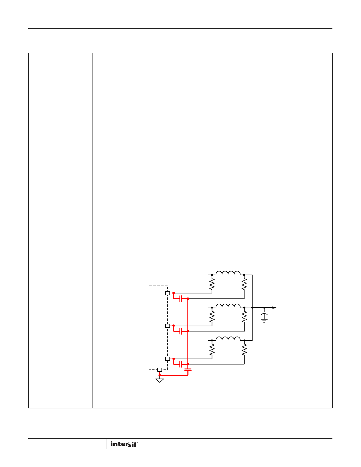
ISL95831
Layout Guidelines
ISL95831
PIN NUMBER SYMBOL LAYOUT GUIDELINES
BOTTOM PAD GND Connect this ground pad to the ground plane through low impedance path. Recommend use of at least 5 vias to connect
to ground planes in PCB internal layers.
1 VWG Place the capacitor (C4) across VW and COMP in close proximity of the controller.
2 NC No special consideration.
3 PGOODG No special consideration.
4, 5, 6 SDA,
ALERT#,
SCLK
7 VR_ON No special consideration.
8 PGOOD No special consideration.
9 NC No special consideration.
10 VR_HOT# No special consideration.
11 NTC The NTC thermistor (R9) needs to be placed close to the thermal source that is monitored to determine CPU Vcore
12 VW Place the capacitor (C4) across VW and COMP in close proximity of the controller.
Follow Intel recommendation.
thermal throttling. Recommend placing it at the hottest spot of the CPU Vcore VR.
13 COMP Place the compensator components (C3, C5, C6 R7, R11, R10 and C11) in general proximity of the controller.
14 FB
15 FB2
ISEN3 Each ISEN pin has a capacitor (Cisen) decoupling it to VSUMN, then through another capacitor (Cvsumn) to GND. Place
16 ISEN2
17 IS EN1
Cisen capacitors as close as possible to the controller and keep the following loops small:
1. Any ISEN pin to another ISEN pin
2. Any ISEN pin to GND
The red traces in the following drawing show the loops that need to minimized.
ISEN3
ISEN2
ISEN1
GND
Cisen
Cisen
Cisen
Phase1
Risen
Phase2
Risen
Phase3
Risen
Vsumn
Cvsumn
L3
L2
L1
Ro
Ro
Ro
V
o
18 VSEN Place the VSEN/RTN filter (C12, C13) in close proximity of the controller for good decoupling.
19 RTN
35
FN7613.0
January 21, 2011
Page 36
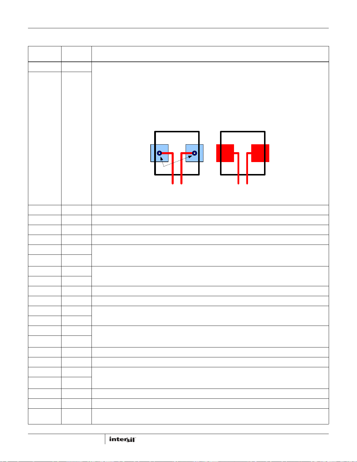
ISL95831
Layout Guidelines (Continued)
ISL95831
PIN NUMBER SYMBOL LAYOUT GUIDELINES
20 ISUMN Place the current sensing circuit in general proximity of the controller.
21 ISUMP
Place capacitor Cn very close to the controller.
Place the NTC thermistor next to VR1 phase-1 inductor (L1) so it senses the inductor temperature correctly.
Each phase of the power stage sends a pair of VSUMP and VSUMN signals to the controller. Run these two signals traces
in parallel fashion with decent width (>20mil).
IMPORTANT: Sense the inductor current by routing the sensing circuit to the inductor pads. Route R63 and R71 to VR1
phase-1 side pad of inductor L1. Route R88 to the output side pad of inductor L1. Route R65 and R72 to VR1 phase-2
side pad of inductor L2. Route R90 to the output side pad of inductor L2. If possible, route the traces on a different layer
from the inductor pad layer and use vias to connect the traces to the center of the pads. If no via is allowed on the pad,
consider routing the traces into the pads from the inside of the inductor. The following drawings show the two preferred
ways of routing current sensing traces.
Inductor
Inductor
Vias
Current-Sensing
Traces
22 VDD A capacitor (C16) decouples it to GND. Place it in close proximity of the controller.
23 VIN A capacitor (C17) decouples it to GND. Place it in close proximity of the controller.
24 PROG1 No special consideration.
25 BOOT1 Use decent wide trace (>30mil). Avoid any sensitive analog signal trace from crossing over or getting close.
Current-Sensing
Traces
26 UGATE1 Run these two traces in parallel fashion with decent width (>30mil). Avoid any sensitive analog signal trace from
27 PHASE1
28 VSSP1 If available, run VSSP1 trace in parallel with LGATE1 trace. Use decent width (>30mil). Avoid any sensitive analog signal
29 LGATE1
30 PWM3 No special consideration.
31 VCCP A capacitor (C22) decouples it to GND. Place it in close proximity of the controller.
32 LGATE2 If available, run VSSP2 trace in parallel with LGATE2 trace. Use decent width (>30mil). Avoid any sensitive analog signal
33 VSSP2
34 PHASE2 Run these two traces in parallel fashion with decent width (>30mil). Avoid any sensitive analog signal trace from
35 UGATE2
36 BOOT2 Use decent wide trace (>30mil). Avoid any sensitive analog signal trace from crossing over or getting close.
37 LGATEG Use decent width (>30mil). Avoid any sensitive analog signal trace from crossing over or getting close.
38 PHASEG Run these two traces in parallel fashion with decent width (>30mil). Avoid any sensitive analog signal trace from
39 UGATEG
40 BOOTG Use decent wide trace (>30mil). Avoid any sensitive analog signal trace from crossing over or getting close.
41 PROG2 No special consideration.
42 NTCG The NTC thermistor needs to be placed close to the thermal source that is monitored to determine AXG Vcore thermal
crossing over or getting close. Recommend routing PHASE1 trace to VR1 phase-1 high-side MOSFET (Q2 and Q8) source
pins instead of general copper.
trace from crossing over or getting close.
trace from crossing over or getting close.
crossing over or getting close. Recommend routing PHASE2 trace to VR1 phase-2 high-side MOSFET (Q4 and Q10)
source pins instead of general copper.
crossing over or getting close. Recommend routing PHASE1G trace to VR2 phase-1 high-side MOSFET source pins
instead of general copper.
throttling. Recommend placing it at the hottest spot of the AXG Vcore VR.
36
FN7613.0
January 21, 2011
Page 37
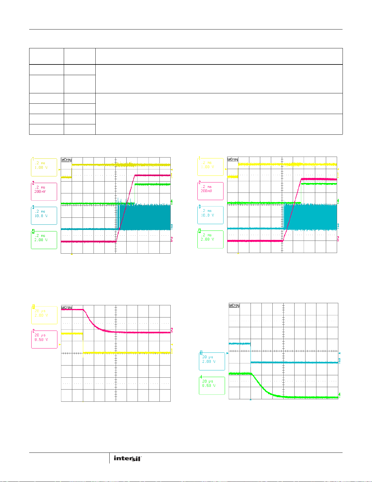
ISL95831
Layout Guidelines (Continued)
ISL95831
PIN NUMBER SYMBOL LAYOUT GUIDELINES
43 ISUMNG Place the current sensing circuit in general proximity of the controller.
44 ISUMPG
45 RTNG Place the VSENG/RTNG filter (C12, C13) in close proximity of the controller for good decoupling.
46 VSENG
47 FBG Place the compensator components (C3, C5, C6 R7, R11, R10 and C11) in general proximity of the controller.
48 COMPG
Place capacitor Cn very close to the controller.
Place the NTC thermistor next to VR2 phase-1 inductor (L1) so it senses the inductor temperature correctly.
See ISUMN and ISUMP pins for layout guidelines of current-sensing trace routing.
Typical Performance
FIGURE 29. VR1 SOFT-START, VIN= 19V, IO= 53A, VID = 1.1V,
Ch1: VR_ON, Ch2: VR1 V
Ch4: PGOOD
FIGURE 31. VR1 SHUT DOWN, V
Ch1: PGOOD, Ch2: VR1 V
, Ch3: PHASE1,
O
=12V, IO= 94A, VID = 1.1V,
IN
O
FIGURE 30. VR2 SOFT-START, V
Ch1: VR_ON, Ch2: VR2 V
Ch4: PGOOD
FIGURE 32. VR1 SHUT DOWN, VIN=12V, IO= 33A, VID = 1.1V,
Ch3: PGOODG, Ch4: VR2 V
=19V, IO= 53A, VID = 1.1V,
IN
, Ch3: PHASE1,
O
O
37
FN7613.0
January 21, 2011
Page 38
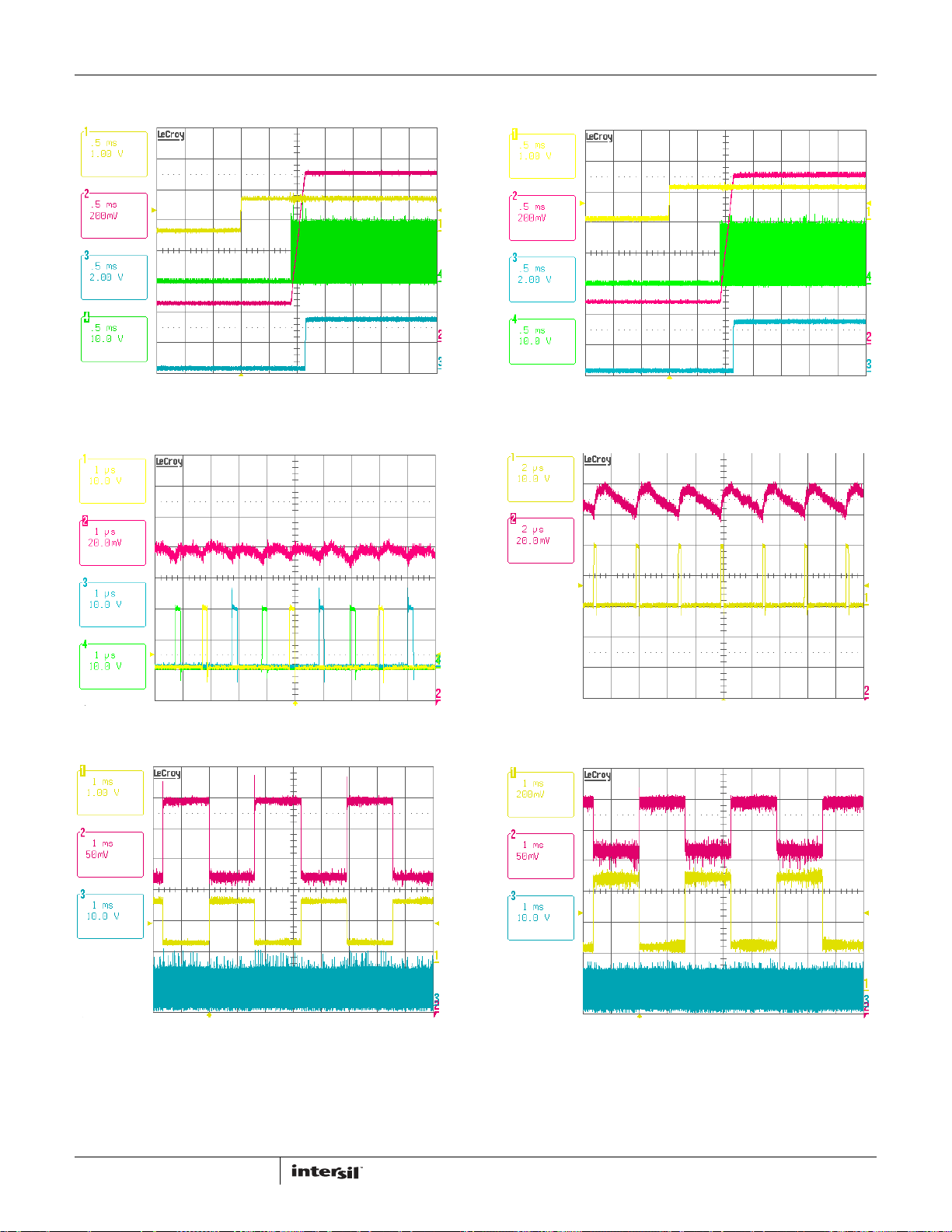
Typical Performance (Continued)
ISL95831
FIGURE 33. VR1 PRE-CHARGED START UP, VIN= 19V,
VID = 1.1V, Ch1: VR_ON, Ch2: VR1 V
Ch4: PHASE1
FIGURE 35. VR1 STEADY STATE, V
Ch1: PHASE1, Ch2: VR1 V
Ch4: PHASE3
=19V, IO= 94A, VID = 1.1V
IN
Ch3: PHASE2,
O,
, Ch3: PGOOD,
O
FIGURE 34. VR2 PRE-CHARGED START UP, V
FIGU RE 36. VR 2 STEA DY STATE, V
VID = 1.1V, Ch1: VR_ON, Ch2: VR2 V
Ch3: PGOODG, Ch4: PHASEG
= 19V, IO= 33A, VID = 1.1V
Ch1: PHASEG, Ch2: VR2 V
IN
O
IN
=19V,
,
O
FIGURE 37. VR1 LOAD TRANSIENT RESPONSE , VIN=19V,
VID = 1.1V, I
LL = 1.9mΩ, Ch1: LOAD CURRENT, Ch2: VR1 V
Ch3: PHASE1
= 28A/94A, di/dt = “FASTEST”,
O
38
FIGURE 38. VR2 LOAD TRANSIENT RESPONSE , V
VID = 1.1V, I
,
O
LL = 3.9mΩ, Ch1: LOAD CURRENT, Ch2: VR2 V
Ch3: PHASEG
= 13A/33A, di/dt = “FASTEST”,
O
=12V,
IN
,
O
FN7613.0
January 21, 2011
Page 39
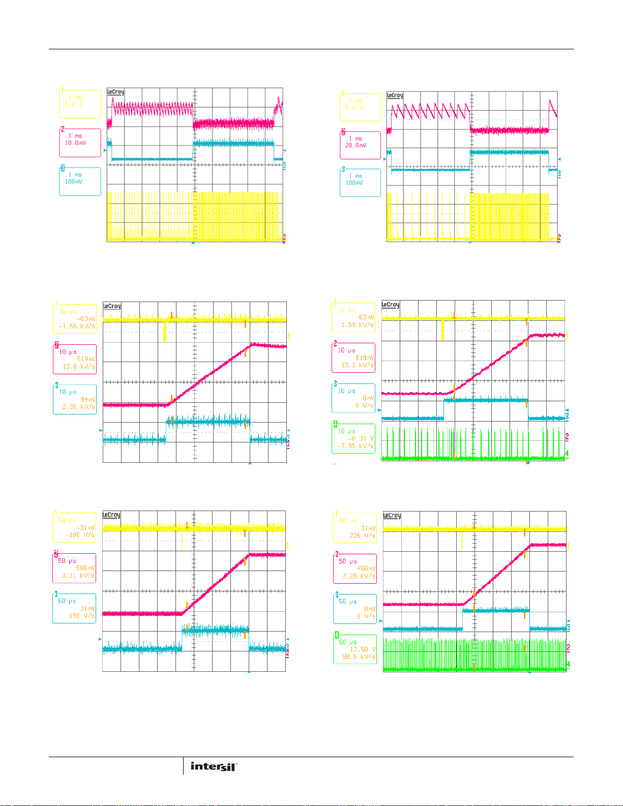
Typical Performance (Continued)
ISL95831
FIGURE 39. VR1 PS2 LOAD TRANSIENT RESPONSE , VIN= 19V,
VID = 0.3V, I
LL = 1.9mΩ, Ch1: PHASE1, Ch2: VR1 V
LOAD CURRENT
FIGURE 41. VR1 SETVID-FAST RESPONSE. I
VID = 0.5V - 1.1V, Ch1: SDA, Ch2: VR1 V
Ch3: ALERT#
= 1A/5A, di/dt = “FASTEST”,
O
= 50A,
O
, Ch3:
O
,
O
FIGURE 40. VR2 PS2 LOAD TRANSIENT RESPONSE , V
VID = 0.3V, I
LL = 3.9mΩ, Ch1: PHASEG, Ch2: VR2 V
LOAD CURRENT
FIGURE 42. VR2 SETVID-FAST RESPONSE. I
VID = 0.5V - 1.1V, Ch1: SDA, Ch2: VR2 V
Ch3: ALERT#, Ch4: PHASEG
= 1A/5A, di/dt = “FASTEST”,
O
=10A,
O
IN
, Ch3:
O
,
O
=12V,
FIGURE 43. VR1 SETVID-SLOW RESPONSE. I
VID = 0.5V - 1.1V, Ch1: SDA, Ch2: VR1 V
Ch3: ALERT#, Ch2: V
, Ch3: PHASE2, Ch4: PHASE3
O
39
=50A,
O
FIGURE 44. VR2 SETVID-SLOW RESPONSE. I
,
O
VID = 0.5V - 1.1V, Ch1: SDA, Ch2: VR2 V
ALERT#, Ch4: PHASEG
= 10A,
O
January 21, 2011
, Ch3:
O
FN7613.0
Page 40
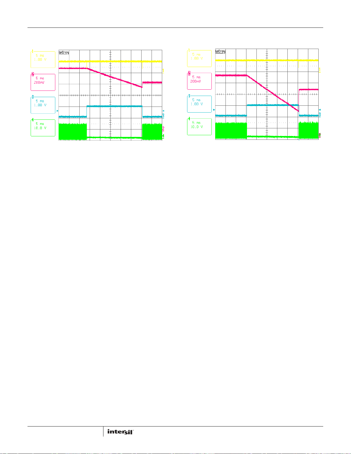
Typical Performance (Continued)
ISL95831
FIGURE 45. VR1 SETVID DECAY PRE_EMPTIVE BEHAVIOR.
SETVID-FAST 0.85V AFTER SETVID DECAY, I
Ch1: SDA, Ch2: VR1 V
Ch4: PHASE1
, Ch3: ALERT#,
O
O
=0A,
FIGURE 46. VR2 SETVID DECAY PRE_EMPTIVE BEHAVIOR.
SETVID-FAST 0.85V AFTER SETVID DECAY, I
Ch1: SDA, Ch2: VR1 V
Ch4: PHASEG
, Ch3: ALERT#,
O
O
=0A,
40
FN7613.0
January 21, 2011
Page 41

ISL95831
Revision History
The revision history provided is for informational purposes only and is believed to be accurate, but not warranted. Please go to web to make
sure you have the latest Rev.
DATE REVISION CHANGE
1/21/11 FN7613.0 Initial Release.
Products
Intersil Corporation is a leader in the design and manufacture of high-performance analog semiconductors. The Company's products
address some of the industry's fastest growing markets, such as, flat panel displays, cell phones, handheld products, and notebooks.
Intersil's product families address power management and analog signal processing functions. Go to www.intersil.com/products for a
complete list of Intersil product families.
*For a complete listing of Applications, Related Documentation and Related Parts, please see the respective device information page
on intersil.com: ISL95831
To report errors or suggestions for this datasheet, please go to: www.intersil.com/askourstaff
FITs are available from our website at: http://rel.intersil.com/reports/sear
For additional products, see www.intersil.com/product_tree
Intersil products are manufactured, assembled and tested utilizing ISO9000 quality systems as noted
Intersil products are sold by description only. Intersil Corporation reserves the right to make changes in circuit design, software and/or specifications at any time
without notice. Accordingly, the reader is cautioned to verify that data sheets are current before placing orders. Information furnished by Intersil is believed to be
accurate and reliable. However, no responsibility is assumed by Intersil or its subsidiaries for its use; nor for any infringements of patents or other rights of third
parties which may result from its use. No license is granted by implication or otherwise under any patent or patent rights of Intersil or its subsidiaries.
41
in the quality certifications found at www.intersil.com/design/quality
For information regarding Intersil Corporation and its products, see www.intersil.com
FN7613.0
January 21, 2011
Page 42
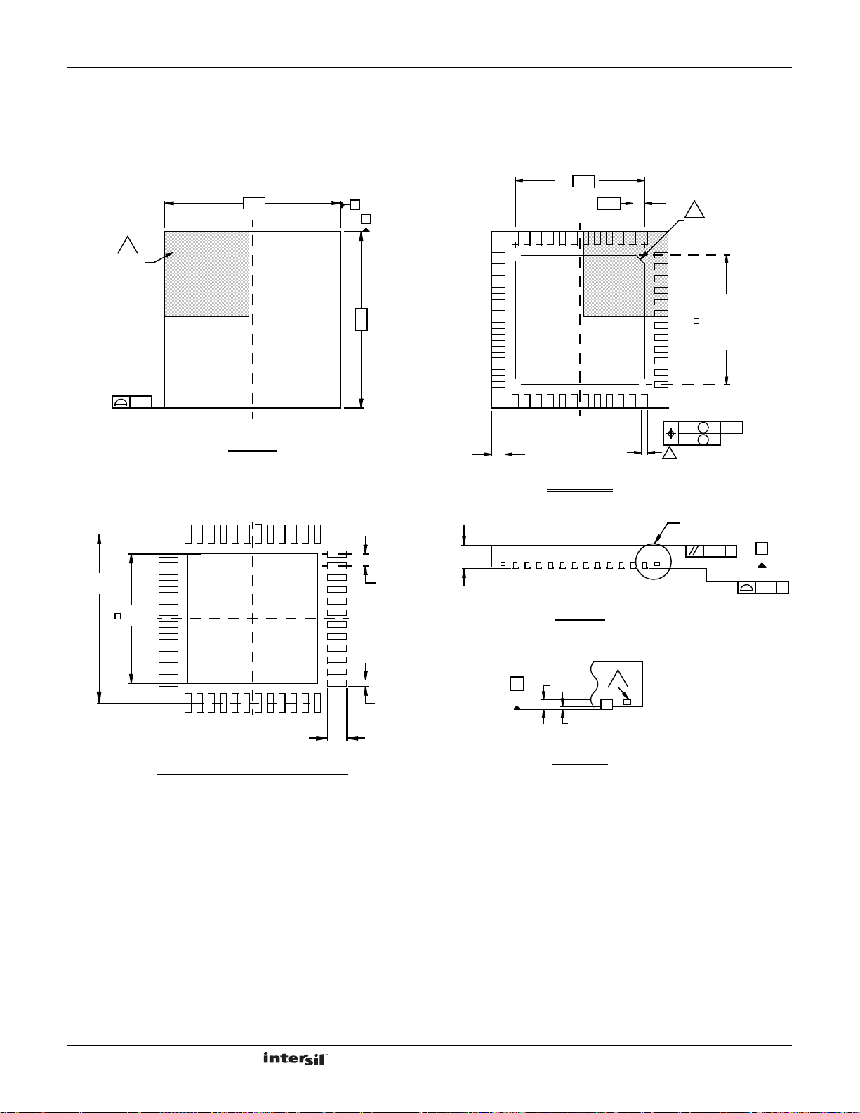
Package Outline Drawing
L48.6x6
48 LEAD THIN QUAD FLAT NO-LEAD PLASTIC PACKAGE
Rev 1, 4/07
6
PIN 1
INDEX AREA
6.00
A
B
ISL95831
4X
4.4
0.40
44X
37
36
48
6
PIN #1 INDEX AREA
1
(4X)
( 5. 75 TYP )
0.15
( 4. 40 )
TOP VIEW
TYPICAL RECOMMENDED LAND PATTERN
6.00
( 44 X 0 . 40 )
( 48X 0 . 20 )
( 48X 0 . 65 )
MAX 0.80
4 .40 ± 0.15
25
24
48X 0.45 ± 0.10
BOTTOM VIEW
SIDE VIEW
0 . 2 REF
C
0 . 00 MIN.
0 . 05 MAX.
5
12
13
4
0.10 CM
0.05 M
48X 0.20
SEE DETAIL "X"
BASE PLANE
AB
C
C
0.10
SEATING PLANE
C
0.08 C
DETAIL "X"
42
NOTES:
Dimensions are in millimeters.1.
Dimensions in ( ) for Reference Only.
2.
Dimensioning and tolerancing conform to AMSE Y14.5m-1994.
3.
Unless otherwise specified, tolerance : Decimal ± 0.05
4.
Dimension b applies to the metallized terminal and is measured
between 0.15mm and 0.30mm from the terminal tip.
Tiebar shown (if present) is a non-functional feature.
5.
The configuration of the pin #1 identifier is optional, but must be
6.
located within the zone indicated. The pin #1 indentifier may be
either a mold or mark feature.
FN7613.0
January 21, 2011
Page 43

 Loading...