

®
ISL9203R5220
Data Sheet January 3, 2006
Li-ion/Li Polymer Battery Charger
The ISL9203R5220 is an integrated single-cell Li-ion or
Li-polymer battery charger capable of operating with an input
voltage as low as 2.4V. This charger is designed to work with
various types of AC adapters.
The ISL9203R5220 operates as a linear charger when the
AC adapter is a voltage source. The battery is charged in a
CC/CV (constant current/constant voltage) profile. The
charge current is programmable with an external resistor up
to 1.5A. The ISL9203R5220 can also work with a currentlimited adapter to minimize the thermal dissipation, in which
case the ISL9203R5220 combines the benefits of both a
linear charger and a pulse charger.
The ISL9203R5220 features charge current thermal
foldback to guarantee safe operation when the printed circuit
board is space limited for thermal dissipation. Additional
features include preconditioning of an over-discharged
battery and thermally enhanced DFN package.
FN9242.1
Features
• Complete Charger for Single-Cell Li-ion Batteries
• Very Low Thermal Dissipation
• Integrated Pass Element and Current Sensor
• No External Blocking Diode Required
• 1% Voltage Accuracy
• Programmable Current Limit up to 1.5A
• Charge Current Thermal Foldback
• Accepts Multiple Types of Adapters
• Guaranteed operation down to VIN = 2.65V after start up
• Ambient Temperature Range: -20
°C to 70°C
• Thermally-Enhanced DFN Packages
• Pb-Free Plus Anneal Available (RoHS Compliant)
Applications
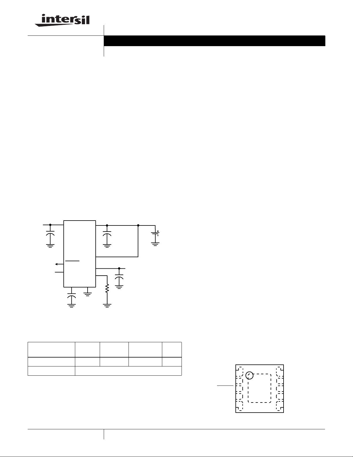
Typical Application Circuit
5V
Input
Floating
to Enable
C
C
TIME
1
STATUS
EN
TIME
VBATVIN
ISL9203
VSEN
GND
V2P8
IREF
R
C
2
IREF
C
3
Ordering Information
PART NUMBER
(Note)
ISL9203CRZR5220 03CZ -20 to 70 10 Ld 3x3 DFN L10.3x3
ISL9203CRZ-TR5220 10 Ld 3x3 DFN Tape and Reel
NOTE: Intersil Pb-free plus anneal products employ special Pb-free material
sets; molding compounds/die attach materials and 100% matte tin plate
termination finish, which are RoHS compliant and compatible with both SnPb
and Pb-free soldering operations. Intersil Pb-free products are MSL
classified at Pb-free peak reflow temperatures that meet or exceed the
Pb-free requirements of IPC/JEDEC J STD-020.
PAR T
MARKING
TEMP.
RANGE (°C)
PACKAGE
(Pb-free)
PKG
DWG. #
• Handheld Devices including Medical Handhelds
• PDAs, Cell Phones and Smart Phones
• Portable Instruments, MP3 Players
• Self-Charging Battery Packs
• Stand-Alone Chargers
• USB Bus-Powered Chargers
Related Literature
• Technical Brief TB363 “Guidelines for Handling and
Processing Moisture Sensitive Surface Mount Devices
(SMDs)”
• Technical Brief TB379 “Thermal Characterization of
Packaged Semiconductor Devices”
• Technical Brief TB389 “PCB Land Pattern Design and
Surface Mount Guidelines for QFN Packages”
Pinout
ISL9203R5220
(3x3 DFN)
TOP VIEW
VIN
NC
STATUS
TIME
GND
1
2
3
4
5
10
VBAT
VSEN
9
IREF
8
V2P8
7
EN
6
1
CAUTION: These devices are sensitive to electrostatic discharge; follow proper IC Handling Procedures.
1-888-INTERSIL or 1-888-468-3774
| Intersil (and design) is a registered trademark of Intersil Americas Inc.
Copyright © Intersil Americas Inc. 2005, 2006. All Rights Reserved.
All other trademarks mentioned are the property of their respective owners.

ISL9203R5220
Absolute Maximum Ratings Thermal Information
Supply Voltage (VIN) . . . . . . . . . . . . . . . . . . . . . . . . . . . . . -0.3 to 7V
Output Pin Voltage (BAT, VSEN, V2P8). . . . . . . . . . . . . -0.3 to 5.5V
Signal Input Voltage (TIME, IREF). . . . . . . . . . . . . . . . . -0.3 to 3.2V
Output Pin Voltage (STATUS) . . . . . . . . . . . . . . . . . . . . . . -0.3 to 7V
Charge Current . . . . . . . . . . . . . . . . . . . . . . . . . . . . . . . . . . . . . 1.6A
ESD Rating
Human Body Model (Per MIL-STD-883 Method 3015.7) . . .4500V
Machine Model (Per EIAJ ED-4701 Method C-111). . . . . . . . 200V
Recommended Operating Conditions
Ambient Temperature Range . . . . . . . . . . . . . . . . . . . . -20°C to 70°C
Supply Voltage, VIN. . . . . . . . . . . . . . . . . . . . . . . . . . . 4.3V to 6.5V
CAUTION: Stresses above those listed in “Absolute Maximum Ratings” may cause permanent damage to the device. This is a stress only rating and operation of the
device at these or any other conditions above those indicated in the operational sections of this specification is not implied.
NOTES:
is measured in free air with the component mounted on a high effective thermal conductivity test board with “direct attach” features. See
1. θ
JA
Tech Brief TB379.
2. θ
, “case temperature” location is at the center of the exposed metal pad on the package underside. See Tech Brief TB379.
JC
Electrical Specifications Typical values are tested at VIN = 5V and 25°C Ambient Temperature, maximum and minimum values are
guaranteed over 0°C to 70°C Ambient Temperature with a supply voltage in the range of 4.3V to 6.5V, unless
otherwise noted.
PARAMETER SYMBOL TEST CONDITIONS MIN TYP MAX UNITS
Thermal Resistance (Typical, Notes 1, 2) θ
(°C/W) θJC (°C/W)
JA
3x3 DFN Package . . . . . . . . . . . . . . . . 46 4
Maximum Junction Temperature (Plastic Package) . . . . . . . . 150°C
Maximum Storage Temperature Range. . . . . . . . . . . -65°C to 150°C
Maximum Lead Temperature (Soldering 10s) . . . . . . . . . . . . . 300°C
POWER-ON RESET
Rising VIN Threshold 3.0 3.4 4.0 V
Falling VIN Threshold 2.3 2.4 2.65 V
STANDBY CURRENT
VBAT Pin Sink Current I
STANDBY
VIN Pin Supply Current I
VIN Pin Supply Current I
VIN
VIN
VIN floating or EN = LOW - - 3.0 µA
VBAT floating and EN pulled low - 30 250 µA
VBAT floating and EN floating - 1 2 mA
VOLTAGE REGULATION
Output Voltage V
CH
4.158 4.20 4.242 V
Dropout Voltage VBAT = 3.7V, Charge current = 1A - 320 550 mV
CHARGE CURRENT
Constant Charge Current (Note 3) I
Constant Charge Current I
Trickle Charge Current I
Trickle Charge Current I
CHARGERIREF
CHARGERIREF
TRICKLE
TRICKLE
End-of-Charge Threshold I
End-of-Charge Threshold I
MIN
MIN
= 80kΩ, V
= 1.21MΩ, V
R
= 80kΩ, V
IREF
R
= 1.21MΩ, V
IREF
R
= 80kΩ 85 110 135 mA
IREF
R
= 1.21MΩ 2-30mA
IREF
= 3.7V 0.9 1.0 1.1 A
BAT
= 3.7V 33 66 100 mA
BAT
= 2.0V 85 110 135 mA
BAT
= 2.0V 2 7 15 mA
BAT
RECHARGE THRESHOLD
Recharge Voltage Threshold V
RECHRG
TRICKLE CHARGE THRESHOLD
Trickle Charge Threshold Voltage V
2
MIN
3.85 4.00 4.10 V
2.7 2.8 3.0 V
FN9242.1
January 3, 2006
ISL9203R5220
Electrical Specifications Typical values are tested at VIN = 5V and 25°C Ambient Temperature, maximum and minimum values are
guaranteed over 0°C to 70°C Ambient Temperature with a supply voltage in the range of 4.3V to 6.5V, unless
otherwise noted. (Continued)
PARAMETER SYMBOL TEST CONDITIONS MIN TYP MAX UNITS
V2P8 PIN VOLTAGE
V2P8 Pin Voltage V
V2P8
TEMPERATURE MONITORING
Charge Current Foldback Threshold (Note 4) T
Current Foldback Gain (Note 5) G
FOLD
FOLD
-100-mA/°C
OSCILLATOR
C
Oscillation Period T
OSC
= 15nF 2.4 3.0 3.6 ms
TIME
LOGIC OUTPUTS
STATUS Logic Low Sink Current Pin Voltage = 0.8V 5 - - mA
STATUS Leakage Current V
VIN
= V
= 5V - - 1 µA
STATUS
EN Input Logic High 2.0 - 3.3 V
EN Input Logic Low --0.8V
EN Pin Current When Driven Low - - 100 µA
NOTES:
3. The accuracy includes all errors except the programming resistance tolerance. The actual charge current may be affected by the thermal
foldback function if the thermal dissipation capability is not enough or by the on resistance of the power MOSFET if the charger input voltage is
too close to the output voltage.
4. Guaranteed by design and characterization to be typically 100°C ±15%
5. Guaranteed by design and characterization.
2.7 2.9 3.1 V
-100- °C
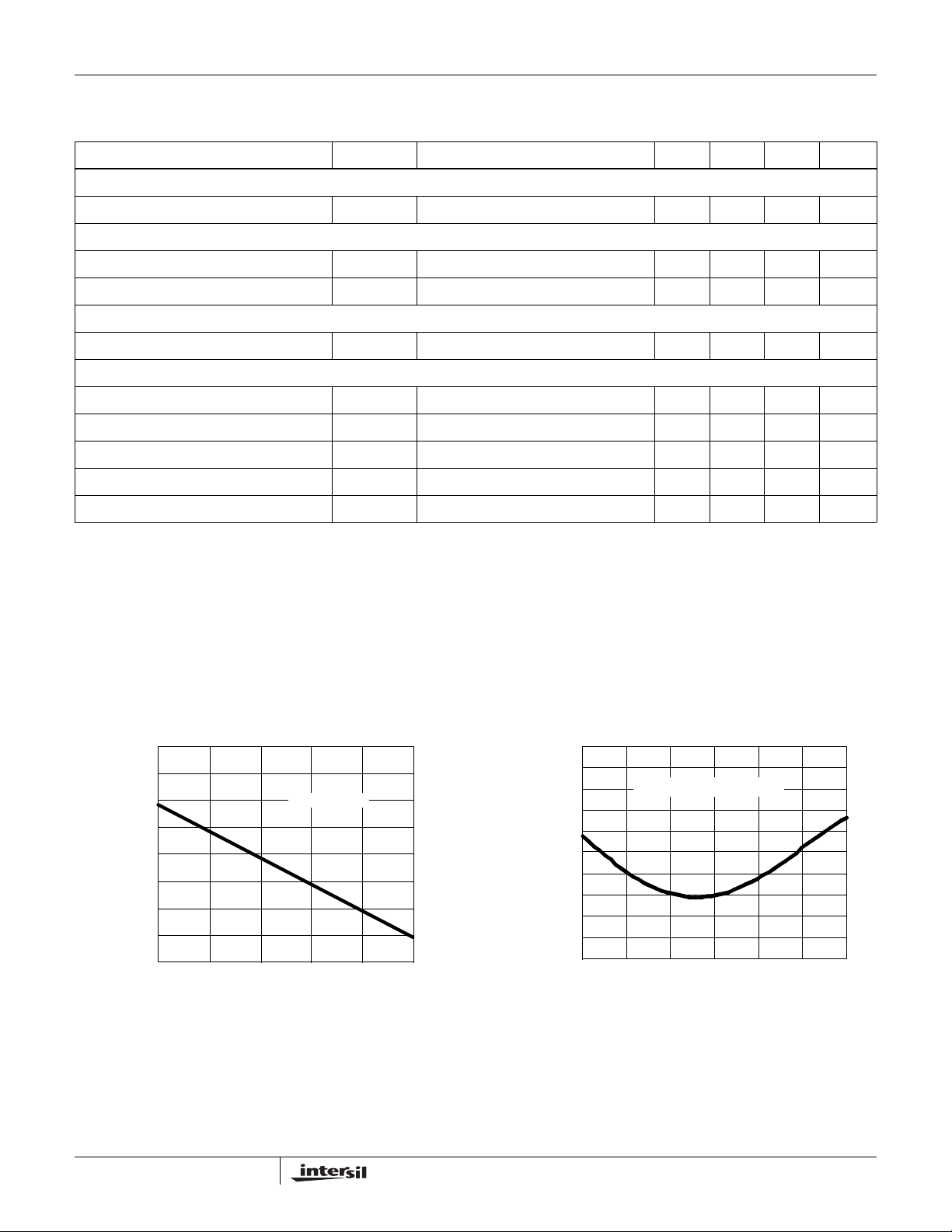
Typical Operating Performance The test conditions for the Typical Operating Performance are: V
= R
R
IREF
4.2015
4.201
R
4.2005
4.2
(V)
4.1995
BAT
V
4.199
4.1985
4.198
4.1975
0 0.3 0.6 0.9 1.2 1.5
CHARGE CURRENT (A)
IREF
= 40kΩ
FIGURE 1. CHARGER OUTPUT VOLTAGE vs CHARGE
CURRENT
IMIN
= 80kΩ, V
= 3.7V, unless otherwise noted.
BAT
4.210
4.208
4.206
4.204
4.202
(V)
4.200
BAT
4.198
V
4.196
4.194
4.192
4.190
0 20 40 60 80 100 120
CHARGE CURRENT = 50mA
TEMPERATURE (°C)
FIGURE 2. CHARGER OUTPUT VOLTAGE vs TEMPERATURE
= 5V, TA = 25°C,
IN
3
FN9242.1
January 3, 2006
ISL9203R5220
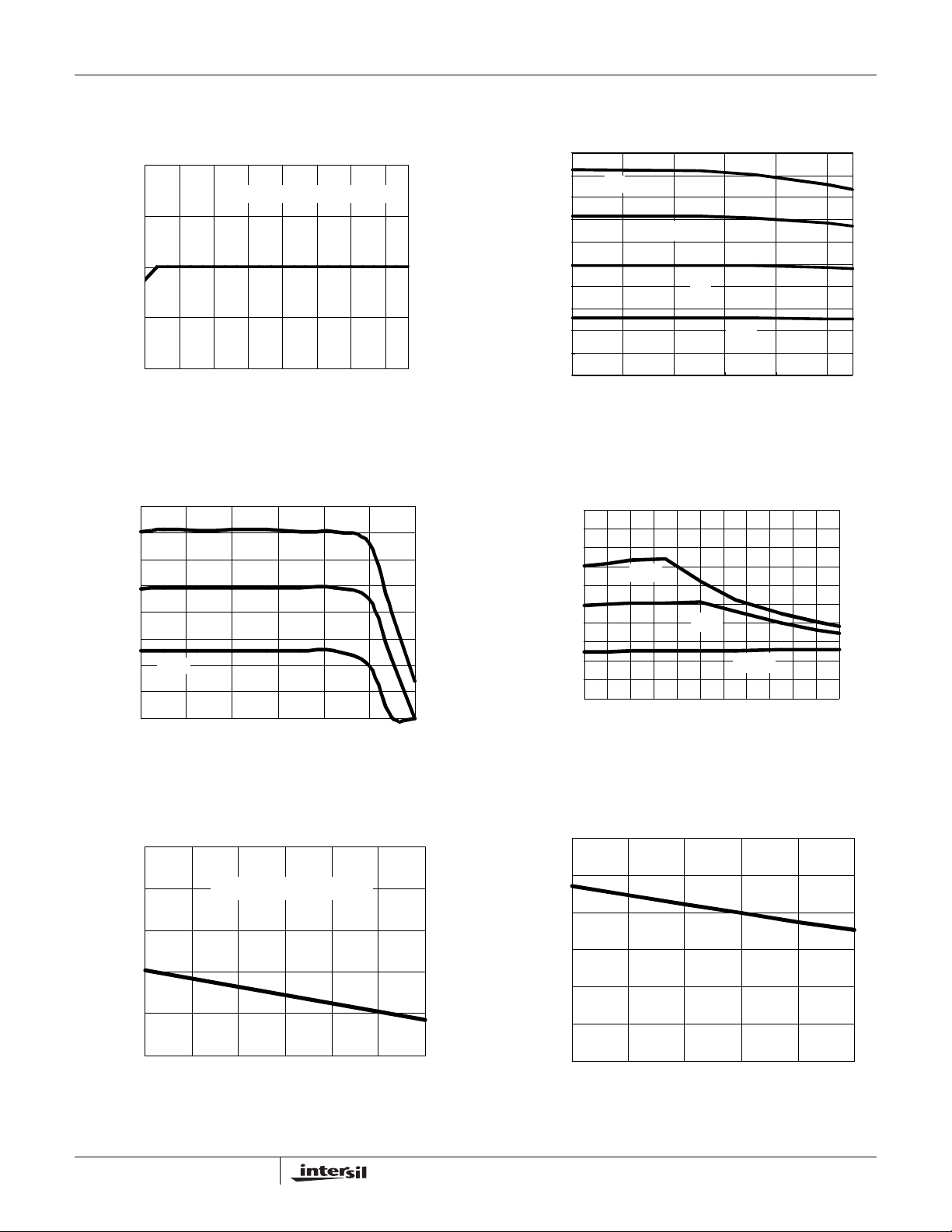
Typical Operating Performance The test conditions for the Typical Operating Performance are: V
R
IREF
4.3
CHARGE CURRENT = 50mA
4.25
(V)
4.2
BAT
V
4.15
4.1
4.2 4.5 4.8 5.1 5.4 5.7 6 6.3
VIN (V)
FIGURE 3. CHARGER OUTPUT VOLTAGE vs INPUT
VOLTAGE CHARGE CURRENT IS 50mA
1.6
1.4
1.2
1.0
0.8
0.6
0.5A
0.4
CHARGE CURRENT (A)
0.2
0.0
0 20 40 60 80 100 120
1.5A
1.0A
TEMPERATURE (°C)
= R
IMIN
= 80kΩ, V
= 3.7V, unless otherwise noted. (Continued)
BAT
2.0
CHARGE CURRENT (A)
1.8
1.6
1.4
1.2
1.0
0.8
0.6
0.4
0.2
0.0
2A
1.5A
3.0 3.2 3.4 3.6 3.8 4.0
FIGURE 4. CHARGE CURRENT vs OUTPUT VOLTAGE
2.0
1.8
1.6
1.4
1.2
1.0
0.8
0.6
0.4
CHARGE CURRENT (A)
0.2
0.0
4.3 4.5 4.7 4.9 5.1 5.3 5.5 5.7 5.9 6.1 6.3 6.5
1.5A
= 5V, TA = 25°C,
IN
1A
V
(V)
VBAT
1A
VIN (V)
0.5A
0.5A
FIGURE 5. CHARGE CURRENT vs AMBIENT TEMPERATURE FIGURE 6. CHARGE CURRENT vs INPUT VOLTAGE
2.93
2.928
)
V
(
E
2.926
G
TA
L
O
2.924
V
8
2P
V
2.922
2.92
3.5 4 4.5 5 5.5 6 6.5
V2P8 PIN LOADED WITH 2mA
V
(V)
IN
3
2.95
2.9
2.85
2.8
V2P8 VOLTAGE (V)
2.75
2.7
0246810
V2P8 LOAD CURRENT (mA)
FIGURE 7. V2P8 OUTPUT vs INPUT VOLTAGE FIGURE 8. V2P8 OUTPUT vs ITS LOAD CURRENT
4
FN9242.1
January 3, 2006
ISL9203R5220
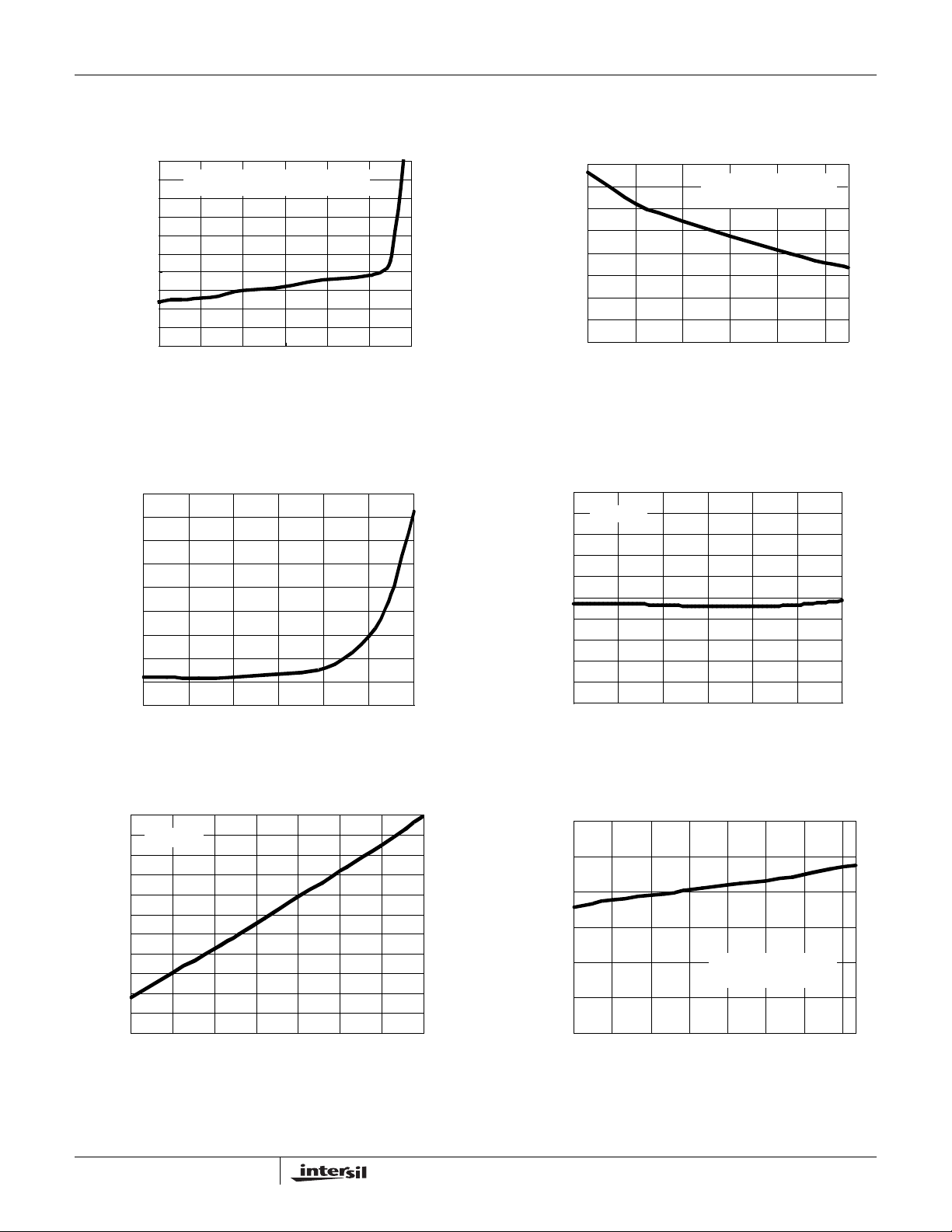
Typical Operating Performance The test conditions for the Typical Operating Performance are: V
= R
R
IREF
700
650
600
550
500
(mΩ)
450
400
DS(ON)
r
350
300
250
200
FIGURE 9. r
1.8
1.6
1.4
1.2
1.0
0.8
0.6
LEAKAGE CURRENT (µA)
0.4
BAT
V
0.2
0.0
THERMAL FOLDBACK STARTS
NEAR 100°C
0 20406080100120
TEMPERAT URE (°C)
vs TEMPERATURE AT 3.7V OUTPUT FIGURE 10. r
DS(ON)
0 20 40 60 80 100 120
TEMPERATURE (°C)
FIGURE 11. REVERSE CURRENT vs TEMPERATURE FIGURE 12.
IMIN
= 80kΩ, V
= 3.7V, unless otherwise noted. (Continued)
BAT
420
400
380
360
(mΩ)
340
320
DS(ON)
r
300
280
260
3.0 3.2 3.4 3.6 3.8 4.0
V
vs OUTPUT VOLTAGE USING CURRENT
DS(ON)
LIMITED ADAPTERS
50
EN = GND
45
40
35
30
25
20
15
QUIESCENT CURRENT (µA)
10
IN
V
5
0
0 20406080100120
TEMPERATURE (°C)
INPUT QUIESCENT CURRENT vs TEMPERATURE
= 5V, TA = 25°C,
IN
500mA CHARGE
CURRENT, R
(V)
BAT
IREF
= 40K
32
30
EN = GND
28
26
24
22
20
18
16
14
QUIESCENT CURRENT (µA)
IN
V
12
10
3.0 3.5 4.0 4.5 5.0 5.5 6.0 6.5
VIN (V)
FIGURE 13. INPUT QUIESCENT CURRENT vs INPUT
VOLTAGE WHEN SHUTDOWN
5
1.10
1.05
1.00
0.95
0.90
QUIESCENT CURRENT (mA)
0.85
IN
V
0.80
4.3 4.6 4.9 5.2 5.5 5.8 6.1 6.4
BOTH VBAT AND EN
PINS FLOATING
VIN (V)
FIGURE 14. INPUT QUIESCENT CURRENT vs INPUT
VOLTAGE WHEN NOT SHUTDOWN
January 3, 2006
FN9242.1

ISL9203R5220
Typical Operating Performance The test conditions for the Typical Operating Performance are: V
= R
R
IREF
28
24
20
16
12
8
4
STATUS PIN CURRENT (mA)
0
0.0 0.5 1.0 1.5 2.0 2.5 3.0 3.5 4.0 4.5 5.0
FIGURE 15. STATUS PIN VOLTAGE vs CURRENT WHEN THE OPEN-DRAIN MOSFET TURNS ON
Pin Descriptions
VIN (Pin1)
VIN is the input power source. Connect to a wall adapter.
NC (Pin 2)
No connection for this pin.
STATUS (Pin 3)
STATUS is an open-drain output indicating charging and
inhibit states. The STATUS pin is pulled LOW when the
charger is charging a battery. It will be forced to high
impedence when the charge current drops to I
impedence mode will be latched until a recharge cycle or a
new charge cycle starts.
TIME (Pin 4)
The TIME pin determines the oscillation period by
connecting a timing capacitor between this pin and GND.
The oscillator also provides a time reference for the charger.
GND (Pin 5)
GND is the connection to system ground.
. This high
MIN
= 80kΩ, V
IMIN
STATUS PIN VOLTAGE (V)
= 3.7V, unless otherwise noted. (Continued)
BAT
EN (Pin 6)
EN is the enable logic input. Connect the EN pin to LOW to
disable the charger or leave it floating to enable the charger.
V2P8 (Pin 7)
This is a 2.8V reference voltage output. This pin outputs a
2.8V voltage source when the input voltage is above POR
threshold, otherwise it outputs zero. The V2P8 pin can be
used as an indication for adapter presence.
IREF (Pin 8)
This is the programming input for the constant charging
current. It maintains at 0.8V when the charger is in normal
operation.
VSEN (Pin 9)
VSEN is the remote voltage sense pin. Connect this pin as
close as possible to the battery pack positive connection. If
the VSEN pin is floating, its voltage drops to zero volt and
the charger operates in the trickle mode.
VBAT (Pin 10)
VBAT is the connection to the battery. Typically a 10µF
Tantalum capacitor is needed for stability when there is no
battery attached. When a battery is attached, only a 0.1µF
ceramic capacitor is required.
= 5V, TA = 25°C,
IN
6
FN9242.1
January 3, 2006

Typical Applications
ISL9203R5220
5V WALL
ADAPTER
Block Diagram
C
1
VBAT
C
2
10µF
BATTERY
PACK
C
1
10µF
R
1kΩ
D
VIN
1
ISL9203R5220
1
VSEN
STATUS
EN
TIME
C
TIME
1nF
VIN
TEMPERATURE
MONITORING
Q
SEN
100000:1
Current
I
T
IREF
R
IREF
I
R
CURRENT
I
SEN
Mirror
+
CA
-
REFERENCES
= IR/10
I
MIN
V2P8
IREF
GND
CHRG
Q
MAIN
V
Input_OK
R
IREF
80kΩ
REFERENCES
CH
POR
MIN
V
V
+
-
+
-
+
VA
-
C
3
1µF
VBAT
V2P8
RECHRG
VIN
V
V
POR
+
100mV
V
CH
VSEN
+
I
SEN
Trickle/Fast
+
-
Input_OK
Minbat
MIN_I
Recharge
LOGIC
-
V
MIN
V
RECHRG
+
-
EN
TIME
GND
VIN
ESD Diode
STATUS
STATUS
OSC
COUNTER
FIGURE 16. BLOCK DIAGRAM
7
FN9242.1
January 3, 2006

Charging Flow Chart
Power Up
VIN>V
?
POR
Y
POR
Initialization
Reset STATUS
Reset counter
ISL9203R5220
N
Trickle
Charge
set STATUS high
Y
Trickle
Charge
VSEN>V
MIN
N
EOC indication:
N
VSEN
<
V
?
RECHRG
N
CC Charge
VSEN>=VCH?
Y
Constant
Current
Charge
N
Y
Constant
Voltage
Charge
CV Charge
Ich < I
?
MIN
N
Y
EOC
EN toggled ?
Y
8
N
FIGURE 17. CHARGING STATE DIAGRAM
FN9242.1
January 3, 2006

ISL9203R5220
Theory of Operation
The ISL9203R5220 is an integrated charger for single-cell
Li-ion or Li-polymer batteries. The ISL9203R5220 functions
as a traditional linear charger when powered with a voltagesource adapter. When powered with a current-limited
adapter, the charger minimizes the thermal dissipation
commonly seen in traditional linear chargers.
As a linear charger, the ISL9203R5220 charges a battery in
the popular constant current (CC) and constant voltage (CV)
profile. The constant charge current I
up to 1.5A with an external resistor. The charge voltage V
has 1% accuracy over the entire recommended operating
condition range. The charger always preconditions the
battery with 10% of the programmed current at the beginning
of a charge cycle, until the battery voltage is verified to be
above the minimum fast charge voltage, V
current preconditioning charge mode is named trickle mode.
The verification takes 15 cycles of an internal oscillator
whose period is programmable with the timing capacitor.
A thermal-foldback feature removes the thermal concern
typically seen in linear chargers. The charger reduces the
charge current automatically as the IC internal temperature
rises above 100°C to prevent further temperature rise. The
thermal-foldback feature guarantees safe operation when
the printed circuit board (PCB) is space limited for thermal
dissipation.
is programmable
REF
. This low-
MIN
CH
HIGH and is latched. The latch is released at the beginning
of a re-charge cycle, when the EN is toggled, or after the
chip is power cycled.
If the ISL9203R5220 has not been power cycled and has not
had the EN pin toggled, but the VSEN voltage drops below
the recharge level, then the device re-enters the charge
mode. In this condition, the charger indicates a re-charge
cycle by bringing the STATUS pin LOW.
When the wall adapter is not present, the ISL9203R5220
draws less than 1
µA of current from the battery.
Figure 18 shows the typical charge curves in a traditional
linear charger powered with a constant-voltage adapter.
From the top to bottom, the curves represent the constant
input voltage, the battery voltage, the charge current and the
power dissipation in the charger. The power dissipation P
CH
is given by the following equation:
P
where I
CH
VINV
–()I
CHARGE
BAT
⋅=
CHARGE
(EQ. 1)
is the charge current. The maximum power
dissipation occurs during the beginning of the CC mode. The
maximum power the IC is capable of dissipating is
dependent on the thermal impedance of the printed-circuit
board (PCB). Figure 18 shows, with dotted lines, two cases
that the charge currents are limited by the maximum power
dissipation capability due to the thermal foldback.
Two indication pins are available from the charger to indicate
the charge status. The V2P8 outputs a 2.8V DC voltage
when the input voltage is above the power-on reset (POR)
level and can be used as a power-present indication. This
pin is capable of sourcing a 2mA current, so it can also be
used to bias external circuits. The STATUS pin is an opendrain logic output that goes LOW at the beginning of a
charge cycle and stays LOW until the end-of-charge (EOC)
condition is qualified. The EOC condition is met when the
battery voltage rises above a recharge threshold and the
charge current falls below an EOC current threshold. Once
the EOC condition is qualified, the STATUS output goes
When using a current-limited adapter, the thermal situation in
the ISL9203R5220 is totally different. Figure 19 shows the
typical charge curves when a current-limited adapter is
employed. The operation requires the I
higher than the limited current I
of the adapter, as shown in
LIM
to be programmed
REF
Figure 19. The key difference of the charger operating under
such conditions occurs during the CC mode.
I
REF
Trickle
V
IN
V
CH
V
MIN
I
REF
/10
P
1
P
2
P
3
Constant Current
Mode
Input Voltage
Mode
Constant Voltage
Mode
Battery Voltage
Charge Current
Power Dissipation
Inhibit
TIMEOUT
FIGURE 18. TYPICAL CHARGE CURVES USING A
CONSTANT-VOLTAGE ADAPTER
9
FN9242.1
January 3, 2006

-
ISL9203R5220
The Block Diagram, Figure 16, aids in understanding the
operation. The current loop consists of the current amplifier
CA and the sense MOSFET Q
. The current reference IR
SEN
is programmed by the IREF pin. The current amplifier CA
regulates the gate of the sense MOSFET Q
sensed current I
main MOSFET Q
matches the reference current IR. The
SEN
and the sense MOSFET Q
MAIN
SEN
so that the
form a
SEN
current mirror with a ratio of 100,000:1, that is, the output
charge current is 100,000 times I
.
R
In the CC mode, the current loop tries to increase the charge
current by enhancing the sense MOSFET Q
, so that the
SEN
sensed current matches the reference current. On the other
hand, the adapter current is limited, the actual output current
will never meet what is required by the current reference. As
a result, the current error amplifier CA keeps enhancing the
Q
as well as the main MOSFET Q
SEN
, until they are
MAIN
fully turned on. Therefore, the main MOSFET becomes a
power switch instead of a linear regulation device. The
power dissipation in the CC mode becomes:
P
CHRDS ON()ICHARGE
where R
DS(ON)
⋅=
is the resistance when the main MOSFET is
2
(EQ. 2)
fully turned on. This power is typically much less than the
peak power in the traditional linear mode.
The worst power dissipation when using a current-limited
adapter typically occurs at the beginning of the CV mode, as
shown in Figure 19. The equation 1 applies during the CV
mode. When using a very small PCB whose thermal
impedance is relatively large, it is possible that the internal
temperature can still reach the thermal foldback threshold. In
that case, the IC is thermally protected by lowering the
charge current, as shown by the dotted lines in the charge
current and power curves. Appropriate design of the adapter
can further reduce the peak power dissipation of the
Trickle
V
IN
V
CH
V
MIN
I
REF
I
LIM
I
/10
REF
Mode
Constant Current
Mode
Input Voltage
Constant Voltage
Mode
Battery Voltage
Charge Current
EOC
ISL9203R5220. See the Application Information section of
the ISL6292 data sheet (www.intersil.com) for more
information.
Figure 20 illustrates the typical signal waveforms for the
linear charger from the power-up to a recharge cycle. More
detailed Applications Information is given below.
Applications Information
Power on Reset (POR)
The ISL9203R5220 resets itself as the input voltage rises
above the POR rising threshold. The V2P8 pin outputs a
2.8V voltage, the internal oscillator starts to oscillate, the
internal timer is reset, and the charger begins to charge the
battery. The STATUS pin indicates a LOW logic signal.
Figure 20 illustrates the start up of the charger between t
t
.
2
The ISL9203R5220 has a typical rising POR threshold of
3.4V and a falling POR threshold of 2.4V. The 2.4V falling
threshold guarantees charger operation with a currentlimited adapter to minimize the thermal dissipation.
Charge Cycle
A charge cycle consists of three charge modes: trickle mode,
constant current (CC) mode, and constant voltage (CV)
mode. The charge cycle always starts with the trickle mode
until the battery voltage stays above V
15 consecutive cycles of the internal oscillator. If the battery
voltage drops below V
during the 15 cycles, the 15-cycle
MIN
counter is reset and the charger stays in the trickle mode.
The charger moves to the CC mode after verifying the
battery voltage is above V
MIN
.
When the battery-pack terminal voltage rises to the final
charge voltage V
, the CV mode begins. The terminal
CH
voltage is regulated at the constant V
the charge current declines. After the charge current drops
below I
MIN
(1/10 of I
, see Section “End-of-Charge (EOC)
REF
Current” for more detail) the ISL9203R5220 indicates the
end-of-charge with the STATUS pin. The charging operation
does not terminate. Signals in a charge cycle are illustrated
in Figure 20 between points t
to t5.
2
The end of charge indicator (STATUS) will not be set if the
charging current is below I
V
exceeds the V
BAT
still below I
MIN
RECHRG
after these 16 cycles, STATUS goes high to
within the first 16 cycles after
MIN
voltage. If the charge current is
indicate end of charge.
The following events initiate a new charge cycle:
(2.8V typical) for
MIN
in the CV mode and
CH
to
0
P
1
P
2
FIGURE 19. TYPICAL CHARGE CURVES USING A CURRENT
LIMITED ADAPTER
Power Dissipation
10
• POR,
• the battery voltage drops below a recharge threshold,
• or, the EN pin is toggled from GND to floating.
Further description of these events are given later in this
data sheet.
FN9242.1
January 3, 2006

ISL9203R5220
Recharge
After a charge cycle completes, the charger continues to
regulate the output at the constant voltage; but the STATUS
pin indicates that the charging is completed. The STATUS
pin stays high until the battery voltage drops to below the
recharge threshold, V
RECHRG
(see Electrical
Specifications). Then the STATUS pin goes low and a new
charge cycle starts at point t
point t
with the STATUS pin again going high, as shown in
7
. The charge cycle ends at
6
Figure 20.
VIN
POR Threshold
V2P8
STATUS
VBAT
I
CHARGE
Charge Cycle
At least 15
Cycles
V
2.8V V
t0t1t2t
FIGURE 20. OPERATION WAVEFORMS
t
3
RECHRG
MIN
4t5
I
MIN
Charge Cycle
t
6
t
7
Internal Oscillator
The internal oscillator establishes a timing reference. The
oscillation period is programmable with an external timing
capacitor, C
oscillator charges the timing capacitor to 1.5V and then
discharges it to 0.5V in one period, both with 10µA current.
The period T
, as shown in Typical Applications. The
TIME
is:
OSC
Table 1 shows the charge current vs. selected R
IREF
values.
The typical trickle charge current is 10% of the programmed
constant charge current. Table 2 shows the trickle charge
current tolerance guidance at given R
values, when the
IREF
battery voltage is between 0V to 2.5V.
TABLE 1. CHARGE CURRENT vs R
CHARGE CURRENT (mA)
(kΩ)
R
IREF
267 ~ 160 17% lower than
160 450 500 550
100 720 800 880
88.9 810 900 990
80 900 1000 1100
TABLE 2. TRICKLE CHARGE CURRENT vs R
(kΩ)
R
IREF
267 15 30 60
160 30 50 80
100 40 80 120
88.9 45 90 135
80 70 100 150
NOTE: The values in table 2 and table 1 are not tested and are only
for guidance in selecting resistor values for mass production tests or
in customer’s products.
MIN TYP MAX
= I
TYP Value
TRICKLE CHARGE CURRENT (mA)
MIN TYP MAX
REF
in EQ. 5
VALUES.
IREF
17% higher than
IREF
TYP Value
VAL U E S.
End-of-Charge (EOC) Current
The EOC current I
starts to indicate the end of the charge with the STATUS pin,
as shown in Figure 20. The charger actually does not
terminate charging. In the ISL9203R5220, the EOC current
is internally set to 1/10 of the CC charge current, that is,
sets the level at which the charger
MIN
T
OSC
0.2 106C
⋅⋅= ondssec()
TIME
(EQ. 3)
A 1nF capacitor results in a 0.2ms oscillation period.The
accuracy of the period is mainly dependent on the accuracy
of the capacitance and the internal current source.
Charge Current Programming
The charge current in the CC mode is programmed by the
IREF pin. The voltage of IREF is regulated to a 0.8V
reference voltage. The charging current during the constant
current mode is 100,000 times that of the current in the
R
resistor. Hence, the charge current is,
IREF
I
REF
=
0.8V
-----------------
R
IREF
5
× A()
10
(EQ. 4)
11
1
------
I
MIN
10
⋅=
I
REF
(EQ. 5)
At the EOC, the STATUS signal rises to HIGH and is latched.
The latch is not reset until a recharge cycle or a new charge
cycle starts. The tolerance guidance for the EOC current at
selected R
R
IREF
267 15 30 60
160 30 50 80
100 40 80 120
88.9 45 90 135
values are given in Table 3.
IREF
TABLE 3. EOC CURRENT vs R
EOC CURRENT (mA)
(kΩ)
MIN TYP MAX
IREF
VALUES.
January 3, 2006
FN9242.1

T
ISL9203R5220
TABLE 3. EOC CURRENT vs R
EOC CURRENT (mA)
(kΩ)
R
IREF
80 70 100 150
FIGURE 21. CURRENT SIGNALS AT THE AMPLIFIER CA INPU
NOTE: The values in table 3 are not tested and are only for guidance
in selecting resistor values for mass production tests or in customer’s
products.
MIN TYP MAX
IREF
I
R
TEMPERATURE100OC
VALUES.
I
T
I
SEN
Charge Current Thermal Foldback
Over-heating is always a concern in a linear charger. The
maximum power dissipation usually occurs at the beginning
of a charge cycle when the battery voltage is at its minimum
but the charge current is at its maximum. The charge current
thermal foldback function in the ISL9203R5220 frees users
from the over-heating concern.
Figure 21 shows the current signals at the summing node of
the current error amplifier CA in the Block Diagram. I
reference. I
block. The I
is the current from the Temperature Monitoring
T
has no impact on the charge current until the
T
internal temperature reaches approximately 100°C; then I
rises at a rate of 1µA/°C. When I
loop forces the sensed current I
rises, the current control
T
to reduce at the same
SEN
is the
R
T
rate. As a mirrored current, the charge current is 100,000
times that of the sensed current and reduces at a rate of
100mA/°C. For a charger with the constant charge current
set at 1A, the charge current is reduced to zero when the
internal temperature rises to 110°C. The actual charge
current settles between 100°C to 110°C.
Usually the charge current should not drop below I
MIN
because of the thermal foldback. For some extreme cases if
that does happen, the charger does not indicate end-ofcharge unless the battery voltage is already above the
recharge threshold.
2.8V Bias Voltage
The ISL9203R5220 provides a 2.8V voltage for biasing the
internal control and logic circuit. This voltage is also
available for external circuits such as the NTC thermistor
circuit. The maximum allowed external load is 2mA.
3.4V
2.4V
2.8V
V
IN
V2P8
FIGURE 22. THE V2P8 PIN OUTPUT vs THE INPUT VOLTAGE
AT THE VIN PIN. VERTICAL: 1V/DIV,
HORIZONTAL: 100ms/DIV
Indications
The ISL9203R5220 has two indications: the input presence
and the charge status. The input presence is indicated by
the V2P8 pin and the charge status is indicated by the
STATUS pin. Figure 22 shows the V2P8 pin voltage vs. the
input voltage.
STATUS Pull-Up Resistor
The STATUS pin is an open-drain output that need an
external pull-up resistor. It is recommended that this be
pulled up to the input voltage or the 2.8V from the V2P8 pin.
If the STSTUS pin has to be pulled up to other voltages, the
user needs to examine carefully whether or not the ESD
diodes will form a leakage current path to the battery when
the input power is removed. If the leakage path does exist,
an external transistor is required to break the path.
Figure 23 shows the implementation. If the STATUS pin is
directly pulled up to the VCC voltage (not shown in Figure 23),
a current will flow from the VCC to the STATUS pin, then
through the ESD diode to the VIN pin. Any leakage on the VIN
pin, caused by an external or internal current path, will result
in a current path from VCC to ground.
The N-channel MOSFET Q
gate of Q
is connected to VIN or the V2P8 pin. When the
1
STATUS pin outputs a logic low signal, Q
buffers the STATUS pin. The
1
is turned on and
1
its drain outputs a low signal as well. When STATUS is high
impedance, R
power is removed, the Q
the Q
drain stays high.
1
pulls the Q1 drain to high. When the input
1
gate voltage is also removed, thus
1
Shutdown
The ISL9203R5220 can be shutdown by pulling the EN pin
to ground. When shut down, the charger draws typically less
than 30µA current from the input power and the 2.8V output
at the V2P8 pin is also turned off. The EN pin needs be
12
FN9242.1
January 3, 2006

VIN
R
LKG
EN
Control
ESD Diode
GND
Note:
is approximately 240k when EN is floating and is
R
LKG
approximately 140k when the EN is grounded.
STATUS
VCC
VIN or
V2P8
ISL9203R5220
on the 3x3 DFN package are on only two sides, as much top
layer copper as possible should be connected to the
exposed pad to minimize the thermal impedance. Refer to
the ISL6292 evaluation boards for layout examples.
R
1
Q
1
FIGURE 23. PULL-UP CIRCUIT TO AVOID BATTERY
LEAKAGE CURRENT IN THE ESD DIODES
driven with an open-drain or open-collector logic output, so
that the EN pin is floating when the charger is enabled. If the
EN pin is driven by an external source, the POR threshold
voltage will be affected.
Input and Output Capacitor Selection
Typically any type of capacitors can be used for the input
and the output. Use of a 0.47µF or higher value ceramic
capacitor for the input is recommended. When the battery is
attached to the charger, the output capacitor can be any
ceramic type with the value higher than 0.1µF. However, if
there is a chance the charger will be used as an LDO linear
regulator, a 10µF tantalum capacitor is recommended. Note
that the charger always steps through the 15-cycle V
MIN
verification time before the charge current rises to the
constant charge current, as discussed earlier. Hence, when
using as an LDO, the system should make sure not to load
the charger heavily until the 15-cycle verification is
completed.
Working with Current-Limited Adapter
The ISL9203R5220 can work with a current-limited adapter
to significantly reduce the thermal dissipation during
charging. Refer to the ISL6292 data sheet, which can be
found at http://www.intersil.com, for more details.
Board Layout Recommendations
The ISL9203R5220 internal thermal foldback function limits
the charge current when the internal temperature reaches
approximately 100°C. In order to maximize the current
capability, it is very important that the exposed pad under the
package is properly soldered to the board and is connected
to other layers through thermal vias. More thermal vias and
more copper attached to the exposed pad usually result in
better thermal performance. On the other hand, the number
of vias is limited by the size of the pad. The 3x3 DFN
package allows 8 vias be placed in two rows. Since the pins
13
FN9242.1
January 3, 2006

ISL9203R5220
Dual Flat No-Lead Plastic Package (DFN)
INDEX
SEATING
(DATUM B)
6
INDEX
AREA
(DATUM A)
NX (b)
5
SECTION "C-C"
6
AREA
C
PLANE
NX L
8
A
D
TOP VIEW
SIDE VIEW
8
7
D2
12
BOTTOM VIEW
D2/2
N-1N
e
(Nd-1)Xe
REF.
(A1)
2X
A3
NX b
5
0.415
0.15
C
E
B
A
NX
E2
E2/2
0.10 MC
0.200
NX b
C
A
0.152XB
0.10 C
C
0.08
k
AB
NX L
L10.3x3
10 LEAD DUAL FLAT NO-LEAD PLASTIC PACKAGE
MILLIMETERS
C
SYMBOL
NOTESMIN NOMINAL MAX
A 0.80 0.90 1.00 A1 - - 0.05 A3 0.20 REF -
b 0.18 0.23 0.28 5,8
D 3.00 BSC D2 1.95 2.00 2.05 7,8
E 3.00 BSC E2 1.55 1.60 1.65 7,8
e 0.50 BSC -
k0.25 - - L0.300.35 0.40 8
N102
Nd 5 3
Rev. 3 6/04
NOTES:
1. Dimensioning and tolerancing conform to ASME Y14.5-1994.
2. N is the number of terminals.
3. Nd refers to the number of terminals on D.
4. All dimensions are in millimeters. Angles are in degrees.
5. Dimension b applies to the metallized terminal and is measured
between 0.15mm and 0.30mm from the terminal tip.
6. The configuration of the pin #1 identifier is optional, but must be
located within the zone indicated. The pin #1 identifier may be
either a mold or mark feature.
7. Dimensions D2 and E2 are for the exposed pads which provide
improved electrical and thermal performance.
8. Nominal dimensions are provided to assist with PCB Land
Pattern Design efforts, see Intersil Technical Brief TB389.
C
L
L
e
CC
FOR ODD TERMINAL/SIDE
TERMINAL TIP
All Intersil U.S. products are manufactured, assembled and tested utilizing ISO9000 quality systems.
Intersil Corporation’s quality certifications can be viewed at www.intersil.com/design/quality
Intersil products are sold by description only. Intersil Corporation reserves the right to make changes in circuit design, software and/or specifications at any time without
notice. Accordingly, the reader is cautioned to verify that data sheets are current before placing orders. Information furnished by Intersil is believed to be accurate and
reliable. However, no responsibility is assumed by Intersil or its subsidiaries for its use; nor for any infringements of patents or other rights of third parties which may result
from its use. No license is granted by implication or otherwise under any patent or patent rights of Intersil or its subsidiaries.
For information regarding Intersil Corporation and its products, see www.intersil.com
14
FN9242.1
January 3, 2006
 Loading...