

Page 1
®
www.BDTIC.com/Intersil
ISL88694
Data Sheet January 21, 2005
SMBus Accelerator (SMA)
The ISL88694 SMBus accelerator (SMA) is a dual active
pull-up bus terminator designed to improve data
transmission speed on SMBus or similar 2-wire serial bus
interfaces. The ISL88694 is also compatible to the I
bus.
The SMA detects rising input transitions with two internal
voltage references and two comparators per channel. After
the voltage on a data line crosses the first threshold
(V
), the boost pull-up current source is activated to
TRIPL
speed transition. After the voltage crosses the second
threshold (V
), the boost pull-up current source is de-
TRIPH
activated, leaving an active pull-up current of 275µA on the
line. When both channels are HIGH, the pull-up current for
both lines is reduced to 100µA to save power. Internal logic
ensures that the active and boost pull-up current sources are
not activated during downward transitions.
The level for V
referred to V
DD
is controlled by a bandgap voltage
TRIPH
. This feature makes the switching behavior
invariant for all power supply voltages between 2.7V and
5.5V.
A noise filter on each channel prevents the circuit from
responding to input transitions that do not exceed a voltagetime threshold. To activate the boost circuit, the input must
exceed V
by 100Vns (typical) (See Figure 10).
TRIPL
The SMA permits operation of the bus at frequencies up to
100kHz, despite the capacitive loads of multiple devices
and/or long PC board traces. Enhanced ESD protection on
the accelerator pins are guaranteed to withstand 8kV ESD
(HBM) events.
The SMBus Accelerator provides an essential function in
SMBus applications because of distributed capacitance of
SMBus and multiple device input capacitances at various
nodes. By incorporating SMA, systems using SMBus or I
can reliably increase their bus load without the risk of data
loss.
2
C serial
2
C
FN8239.1
Features
• Active Termination for SMBus lines
• Enhances System Bus Signal Rise Time
• Increases Bus Capacity While Guaranteeing Data Integrity
• 2.2mA Rise Time Supply Current
• 8kV ESD Protection on SDA and SCL Pins
• Wide Operating Voltage Range: 2.7V to 5.5V
2
• 2-Wire SMBus and I
C Compatible (100kHz)
• Small Package - SOT23-5
• Pin-for-Pin Compatible with the LTC1694
• Pb-Free Available (RoHS Compliant)
Target Applications
•Servers
• Data Acquisition
•Routers
• Battery Chargers
• Portable Instrumentation
• Notebook
•PC
• Facilities Tracking System
Pinout
ISL88694
(5 LD SOT-23)
TOP VIEW
V
DD
GND
N.C.
1
2
3
5
SMBus1
4
SMBus2
Ordering Information
PART NUMBER PACKAGE TEMP RANGE (°C)
ISL88694IH5 5-pin SOT -40 to 85
ISL88694IH5Z (Note) 5-pin SOT (Pb-Free) -40 to 85
Add “-TK” suffix for tape and reel.
NOTE: Intersil Pb-free products employ special Pb-free material
sets; molding compounds/die attach materials and 100% matte tin
plate termination finish, which are RoHS compliant and compatible
with both SnPb and Pb-free soldering operations. Intersil Pb-free
products are MSL classified at Pb-free peak reflow temperatures that
meet or exceed the Pb-free requirements of IPC/JEDEC J STD-020.
1
CAUTION: These devices are sensitive to electrostatic discharge; follow proper IC Handling Procedures.
1-888-INTERSIL or 321-724-7143
| Intersil (and design) is a registered trademark of Intersil Americas Inc.
All other trademarks mentioned are the property of their respective owners.
Copyright Intersil Americas Inc. 2005. All Rights Reserved
Page 2
ISL88694
www.BDTIC.com/Intersil
Pin Descriptions
SOT-23 SYMBOL DESCRIPTION
1V
DD
Supply Voltage
2 GND Ground
3 N.C. No Connect
4 SMBus1 Active Pull-Up for SMBus
5 SMBus2 Active Pull-Up for SMBus
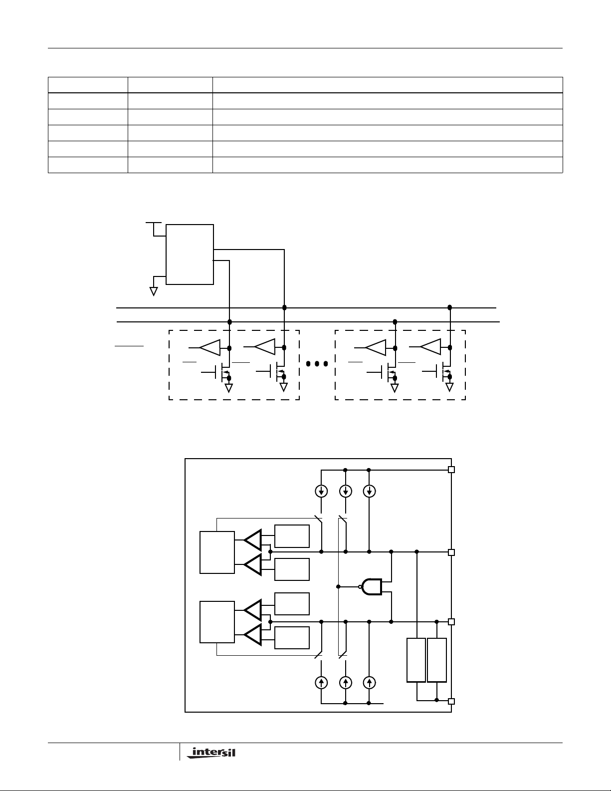
System Diagram
ISL88694
V
DD
SMBus1
SMBus2
GND
BUS SIGNALS
DATA
CLK
Devices;
SBS, PCI,
Compact PCI,
PMCI, ACPI,
ICMB, IPMI,
IPMB,SMBus,
2
C, 2-Wire.
I
IC Block Diagram
Control
Control
DATA IN
OUT
DAT A
CLK IN
CLK
1.825mA
V
TRIPH
+
V
DD
V
V
V
DD
V
-0.5V
TRIPL
0.75V
TRIPH
-0.5V
TRIPL
0.75V
-
+
-
+
-
+
-
175µA100µA
=
=
=
=
CLK IN
OUT
CLK
Device 1 Device N
OUT
DATA IN
OUT
DAT A
V
DD
SMBus1
SMBus2
1.825mA
175µA100µA
2
8kV ESD
8kV ESD
Protection
Protection
V
DD
GND
FN8239.1
January 21, 2005
Page 3
ISL88694
www.BDTIC.com/Intersil
Absolute Maximum Ratings Recommended Operating Conditions
Supply Voltage Range . . . . . . . . . . . . . . . . . . . . . . . . . . . -1V to 6.5V
Operating Junction Temperature . . . . . . . . . . . . . . . . . . . . . . +135°C
Storage Temperature Range . . . . . . . . . . . . . . . . . .-65°C to +150°C
Voltage on pins . . . . . . . . . . . . . . . . . . . . . . . . . .-0.3V to V
Lead temperature (soldering, 10 seconds) . . . . . . . . . . . . . . .300°C
ESD min other pins (HBM). . . . . . . . . . . . . . . . . . . . . . . . . . . . .>2kV
ESD SMBus1 and SMBus2 pins (HBM) . . . . . . . . . . . . . . . . . .>8kV
CAUTION: Absolute Maximum Ratings indicate limits beyond which permanent damage to the device and impaired reliability may occur. These are stress ratings
provided for information only and functional operation of the device at these or any other conditions beyond those indicated in the operational sections of this
specification are not implied.
For guaranteed specifications and test conditions, see Electrical Specifications. The guaranteed specifications apply only for the test conditions listed. Some
performance characteristics may degrade when the device is not operated under the listed test conditions.
DD
+0.3V
Temperature . . . . . . . . . . . . . . . . . . . . . . . . . . . . . . . -40°C to +85°C
Supply Voltage. . . . . . . . . . . . . . . . . . . . . . . . . . . . . . . . 2.7V to 5.5V
Electrical Specifications Over operating conditions unless otherwise specified, Typical values are measured at V
= +25°C
T
A
SYMBOL PARAMETER CONDITIONS MIN TYP MAX UNIT
ANALOG PARAMETERS
V
DD
V
DD RAMPVDD
I
DD
I
OUT_SB
I
OUT_A1
I
OUT_A2
I
OUT_B1
I
OUT_B2
V
TRIPL
V
TRIPH
f
MAX
NSS Noise Spike Suppression
NOTES:
1. Measured as area under triangular waveform above V
Supply Voltage Range 2.7 5.5 V
Ramp Rate 0.05 50 V/msec
Supply Current SMBus1=SMBus2=Open 80 100 µA
Standby Pull-Up Current SMBus1=SMBus2=VDD-1.0V 80 125 µA
Active Pull-Up Current SMBus1=GND; SMBus2=Open 125 275 350 µA
SMBus1= Open; SMBus2=GND 125 275 350 µA
Boost Pull-Up Current (Figure 1) V
Input Voltage Threshold Low 0.65 0.75 0.85 V
Input Voltage Threshold High VDD-0.60 VDD - 0.50 VDD - 0.40 V
SMBus Max Frequency 100 kHz
(Note 1) (Figure 10)
TRIPL
V
TRIPL
<SMBus1<V
<SMBus2<V
, with time as base and VIN as height (See Figure 10).
TRIPL
, SMBus2=Open 1.6 2.2 mA
TRIPH
, SMBus1=Open 1.6 2.2 mA
TRIPH
20 V-nsec
= 3.3V and
DD
3
FN8239.1
January 21, 2005
Page 4

Typical Performance Curves
www.BDTIC.com/Intersil
ISL88694
370
350
(µA)
330
OUT_A
310
290
270
250
230
ACTIVE PULL-UP CURRENT, I
210
-40-20 0 20406080100-60
VDD=5.5V
VDD=2.7V
TEMPERATURE (°C)
FIGURE 1. ACTIVE PULL-UP CURRENT. SMBus PIN=0V
120
110
(µA)
100
OUT_SB
90
80
70
VDD=5.5V
VDD=2.7V
3.75
2.60
(µA)
2.45
OUT_B
2.30
2.15
2.00
1.85
1.70
BOOST PULL-UP CURRENT, I
1.55
-40-20 0 20406080100-60
VDD=5.5V
VDD=2.7V
TEMPERATURE (°C)
FIGURE 2. BOOST PULL-UP CURRENT. SMBus PIN = V
0.95
0.90
(V)
0.85
TRIPL
0.80
0.75
0.70
VDD=5.5V
VDD=2.7V
DD
/2.
60
50
STANDBY PULL-UP CURRENT, I
40
-40-20 0 20406080100-60
TEMPERATURE (°C)
FIGURE 3. STANDBY PULL-UP CURRENT. SMBus1,2=V
DD
-0.5V
0.65
INPUT THRESHOLD LOW, V
0.60
0.55
-40-20 0 20406080100-60
FIGURE 4. V
TEMPERATURE (°C)
VOLTAGE
TRIPL
4
FN8239.1
January 21, 2005
Page 5

Typical Performance Curves (Continued)
www.BDTIC.com/Intersil
ISL88694
0.70
-V)
0.65
DD
(V
0.60
TRIPH
0.55
0.50
0.45
0.40
0.35
INPUT THRESHOLD HIGH, V
0.30
-40-20 0 20406080100-60
TEMPERATURE (°C)
FIGURE 5. V
TRIPH
VDD=5.5V
VDD=2.7V
VOLTAGE
(mA)
3.5
3.0
95
90
85
(µA)
80
DD
75
70
65
SUPPLY CURRENT, I
60
55
FIGURE 6. I
VDD=5.5V
VDD=2.7V
-40-20 0 20406080100-60
TEMPERATURE (°C)
CURRENT. SMBus1=SMBus2=OPEN.
DD
2.5
OUT_B
2.0
1.5
0
VDD=2.7V
123450
SMBus VOLTAGE (V)
1.0
0.5
BOOST PULL-UP CURRENT, I
FIGURE 7. BOOST PULL-UP CURRENT vs. SMBus VOLTAGE
Functional Description
SMBus Overview
The SMBus or I2C bus is a 2-wire multimaster bus, meaning
that more than one device connected to the bus is capable of
controlling it. Master devices communicate to other master
or slave devices using one clock and one data line. These
are both bidirectional.
In order to allow multimaster operation without bus
contention, it is necessary to allow each bus to be connected
to a positive supply voltage via a current-source or pull-up
resistor (see “System Diagram” on page 2). When the bus is
free, both lines are HIGH. The output stages of devices
VDD=5.0V
6
connected to the bus must have an open-drain or opencollector to perform the wired-AND function.
Simple pull-up resistors on the clock and data lines work well
unless there are long signal lines or many devices
connected to the bus. Then, the combined capacitance of
the bus increases the rise time on the signal to such an
extent that the communication becomes unreliable or fails to
meet the bus timing specifications. Smaller resistors can
sometimes compensate for the extra capacitance, but this
increases the current consumption when the signal lines are
pulled LOW.
5
FN8239.1
January 21, 2005
Page 6

ISL88694
www.BDTIC.com/Intersil
ISL88694 Operation
To improve the operation of the SMBus where larger bus
capacitance exists, the ISL88694 provides active pull-up
using switched current sources. When the bus is idle and
both lines are HIGH, a standby pull-up current of 100µA is
used to maintain the signal level while minimizing power
consumption. When either of the two signals is pulled LOW,
an active pull-up current of 275µA maintains a good V
noise margin.
When the bus line is released, it is pulled high by the
ISL88694 active current until the voltage exceeds the
V
level for a period of time. This voltage-time
TRIPL
combination filters out noise on the signal line. Once the
ISL88694 detects a valid rising edge, a 2.2mA boost current
pulls the bus line high very quickly (see Figure 8). This boost
current turns off when the input level reaches the V
threshold and the pull-up current returns to the active level. If
both inputs are HIGH, the pull-up current drops to the
standby level of 100µA.
With ISL88694 SMA
V
TRIPH
OL
TRIPH
With ISL88694 SMA
V
TRIPH
With RC
Pullup
V
TRIPL
R=15.8K
C= 200pF
FIGURE 9. ISL88694 SMBus SYSTEM BOOST PULL-UP
V
DD
V
TRIPH
COMPARED TO RESISTOR PULL-UP (V
2.7V).
With SMA
DD
=
With RC
Pullup
V
TRIPL
R=15.8K
C= 200pF
FIGURE 8. ISL88694 SMBus SYSTEM BOOST PULL-UP
COMPARED TO RESISTOR PULL-UP (V
5.5V).
DD
=
Without SMA
V
TRIPL
>20Vns
Gnd
SMBus1
SMBus2
FIGURE 10. NOISE SUPPRESSION. BOOST CURRENT
APPLIED WHEN INPUT SIGNAL EXCEEDS 20Vns
(TYPICAL).
(Typical)
t
6
FN8239.1
January 21, 2005
Page 7

Package Outline Drawing
www.BDTIC.com/Intersil
0.054 (1.38) BSC
0.065 (1.65)
0.061 (1.55)
4X
0.35 HA-BD
ISL88694
5-Lead, SOT23, Package Code H5
0.108 (2.75) BSC
0.007 (0.20)
B
0.0006 (0.15)
C
L
B
0.35 CA-BD
2X N/2 TIPS
0.033 (0.85)
0.035 (0.90)
0.0008 (0.02)
0.0040 (0.10)
0.043 (1.10) MAX
1
0.075 (1.90) BSC
0.118 (3.00)
0.110 (2.80)
0.038 (0.95)
BSC
3
Parting Line
Seating Plane
0.10 R MIN.
0.20 in
0-8°C
12° REF.
TYP.
0.575 REF.
0.10 R
MIN.
SEATING PLANE
.019 (0.50)
.012 (0.30)
NOTES:
1. ALL DIMENSIONS IN INCHES (IN PARENTHESES IN MILLIMETERS)
2. PACKAGE DIMENSIONS EXCLUDE MOLDING FLASH
3. DIMENSIONING AND TOLERANCES PER ASME, Y14.5-1994
4. THIS PART IS COMPLIANT WITH JEDEC SPECIFICATION MO-193.
5. THIS PART IS FULL COMPLIANCE TO EIAJ SPECIFICATION SC-74
All Intersil U.S. products are manufactured, assembled and tested utilizing ISO9000 quality systems.
Intersil Corporation’s quality certifications can be viewed at www.intersil.com/design/quality
Intersil products are sold by description only. Intersil Corporation reserves the right to make changes in circuit design, software and/or specifications at any time without
notice. Accordingly, the reader is cautioned to verify that data sheets are current before placing orders. Information furnished by Intersil is believed to be accurate and
reliable. However, no responsibility is assumed by Intersil or its subsidiaries for its use; nor for any infringements of patents or other rights of third parties which may result
from its use. No license is granted by implication or otherwise under any patent or patent rights of Intersil or its subsidiaries.
For information regarding Intersil Corporation and its products, see www.intersil.com
7
FN8239.1
January 21, 2005
 Loading...