Intersil ISL62883BHRTZ, ISL62883HRTZ, ISL62883IRTZ Schematic [ru]

Multiphase PWM Regulator for IMVP-6.5™ Mobile CPUs
ISL62883, ISL62883B
The ISL62883 is a multiphase PWM buck regulator for
miroprocessor core power supply. The multiphase buck converter
uses interleaved phase to reduce the total output voltage ripple with
each phase carrying a portion of the total load current, providing
better system performance, superior thermal management, lower
component cost, reduced power dissipation, and smaller
implementation area. The ISL62883 uses two integrated gate
drivers and an external gate driver to provide a complete solution.
The PWM modulator is based on Intersil's Robust Ripple Regulator
3
) technology™. Compared with traditional modulators, the R3™
(R
modulator commands variable switching frequency during load
transients, achieving faster transient response. With the same
modulator, the switching frequency is reduced at light load,
increasing the regulator efficiency.
The ISL62883 is fully compliant with IMVP-6.5™ specifications. It
responds to PSI# and DPRSLPVR signals by adding or dropping
PWM3 and Phase-2 respectively, adjusting overcurrent protection
threshold accordingly, and entering/exiting diode emulation mode.
It reports the regulator output current through the IMON pin. It
senses the current by using either a discrete resistor or inductor
DCR whose variation over temperature can be thermally
compensated by a single NTC thermistor. It uses differential
remote voltage sensing to accurately regulate the processor die
voltage. The adaptive body diode conduction time reduction
function minimizes the body diode conduction loss in diode
emulation mode. User-selectable overshoot reduction function
offers an option to aggressively reduce the output capacitors as
well as the option to disable it for users concerned about
increased system thermal stress. In 2-Phase configuration, the
ISL62883 offers the FB2 function to optimize 1-Phase
performance.
The ISL62883B has the same functions as the ISL62883, but
comes in a different package.
Features
• Precision Multiphase Core Voltage Regulation
- 0.5% System Accuracy Over-Temperature
- Enhanced Load Line Accuracy
• Microprocessor Voltage Identification Input
- 7-Bit VID Input, 0.300V to 1.500V in 12.5mV Steps
- Supports VID Changes On-The-Fly
• Supports Multiple Current Sensing Methods
- Lossless Inductor DCR Current Sensing
- Precision Resistor Current Sensing
• Supports PSI# and DPRSLPVR modes
• Superior Noise Immunity and Transient Response
• Current Monitor and Thermal Monitor
• Differential Remote Voltage Sensing
• High Efficiency Across Entire Load Range
• Programmable 1-, 2- or 3-Phase Operation
• Two Integrated Gate Drivers
• Excellent Dynamic Current Balance Between Phases
• FB2 Function in 2-Phase Configuration to Optimize 1-Phase
Performance
• Adaptive Body Diode Conduction Time Reduction
• User-selectable Overshoot Reduction Function
• Small Footprint 40 Ld 5x5 or 48 Ld 6x6 TQFN Package
• Pb-Free (RoHS Compliant)
Applications
• Notebook Computers
June 21, 2011
FN6891.4
1
CAUTION: These devices are sensitive to electrostatic discharge; follow proper IC Handling Procedures.
1-888-INTERSIL or 1-888-468-3774 | Copyright Intersil Americas Inc. 2009-2011. All Rights Reserved
Intersil (and design) is a trademark owned by Intersil Corporation or one of its subsidiaries.
All other trademarks mentioned are the property of their respective owners.
Ordering Information
ISL62883, ISL62883B
PART NUMBER
(Notes 1, 2, 3)
PART
MARKING
TEMP. RANGE
(°C)
PACKAGE
(Pb-Free)
PKG.
DWG. #
ISL62883HRTZ 62883 HRTZ -10 to +100 40 Ld 5x5 TQFN L40.5x5
ISL62883IRTZ 62883 IRTZ -40 to +100 40 Ld 5x5 TQFN L40.5x5
ISL62883BHRTZ 62883 BHRTZ -10 to +100 48 Ld 6x6 TQFN L48.6x6
NOTES:
1. Add “-T*” suffix for tape and reel. Please refer to TB347
for details on reel specifications.
2. These Intersil Pb-free plastic packaged products employ special Pb-free material sets, molding compounds/die attach materials, and 100% matte
tin plate plus anneal (e3 termination finish, which is RoHS compliant and compatible with both SnPb and Pb-free soldering operations). Intersil Pbfree products are MSL classified at Pb-free peak reflow temperatures that meet or exceed the Pb-free requirements of IPC/JEDEC J STD-020.
3. For Moisture Sensitivity Level (MSL), please see device information page for ISL62883
TB363
.
, ISL62883B. For more information on MSL please see techbrief
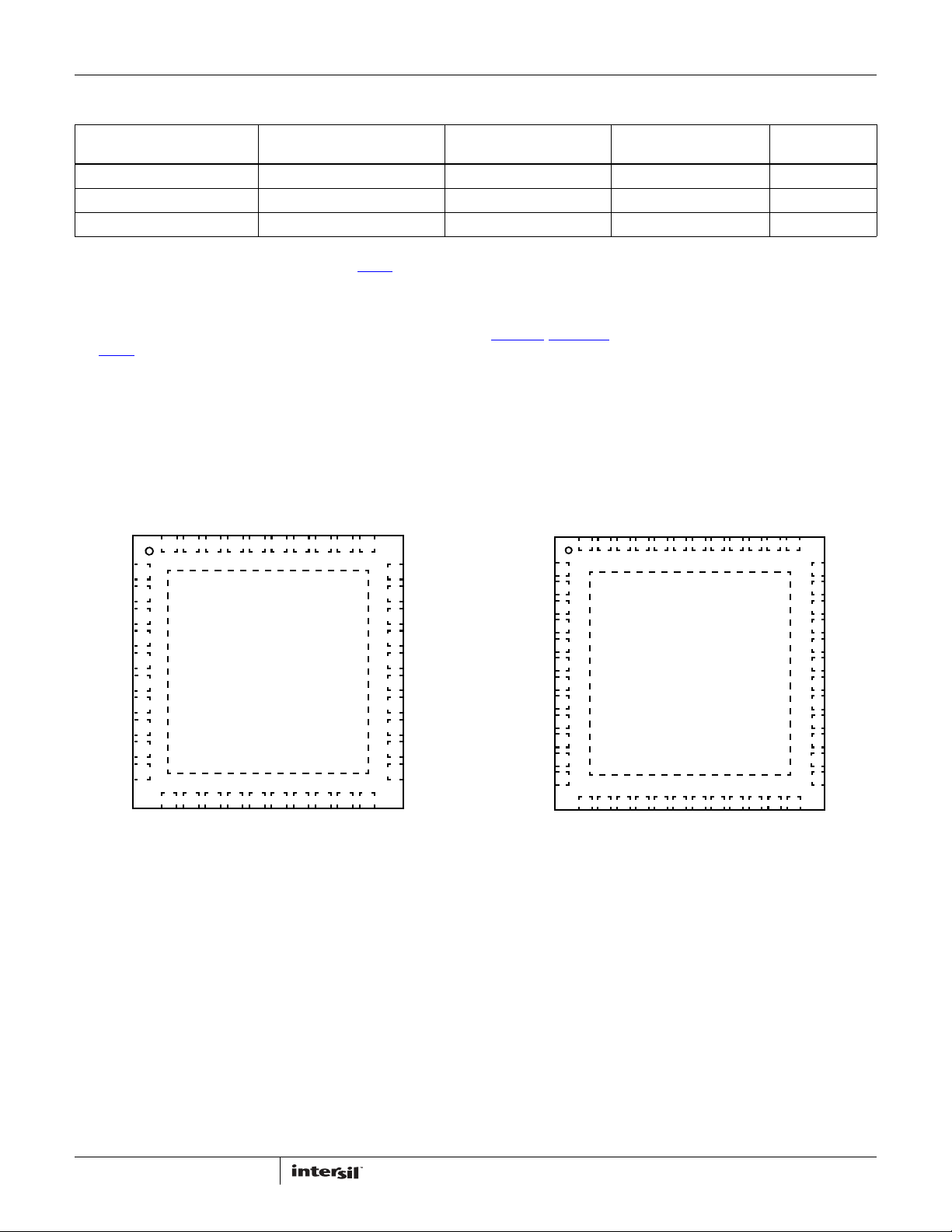
Pin Configurations
N#
_E
CLK
ISEN1
R
LPV
PRS
D
VSEN
ISL62883B
(48 LD TQFN)
TOP VIEW
6
_ON
VR
RTN
VID
VID5
(BOTTOM)
ISUM-
ISUM+
D4
VI
VDD
ID3VID2
V
NC
VIN
D1
VI
IMON
ID0
V
38 37
23 24
NC
NC
36
35
34
33
32
31
30
29
28
27
26
25
BOOT1
BOOT2
UGATE2
PHASE2
VSSP2
LGATE2
NC
VCCP
PWM3
LGATE1
VSSP1
PHASE1
UGATE1
PGOOD
PSI#
RBIAS
VR_TT#
NTC
VW
COMP
FB
SEN3/FB2
ISEN2
ISL62883
(40 LD TQFN)
TOP VIEW
R
V
#
P
N
L
N
E
S
_
O
R
_
K
L
P
R
V
C
D
39 38 37 36 35 34 33 32 31
40
1
2
3
4
5
6
7
8
9
10
11 12 13 14 15 16 17 18 19 20
RTN
VSEN
ISEN1
6
5
D
D
I
I
V
V
GND PAD
(BOTTOM)
ISUM-
ISUM+
4
D
I
V
VDD
2
1
3
D
I
V
VIN
D
I
V
IMON
0
D
D
I
I
V
V
BOOT1
UGATE1
30
29
28
27
26
25
24
23
22
21
BOOT2
UGATE2
PHASE2
VSSP2
LGATE2
VCCP
PWM3
LGATE1
VSSP1
PHASE1
NC
PGOOD
PSI#
RBIAS
VR_TT#
NTC
GND
VW
COMP
FB
ISEN3/FB2
NC
NC
48
47 46 45 44 43 42 41 40 39
1
2
3
4
5
6
7
8
9
10
11
12
13 14 15 16 17 18 19 20 21 22
ISEN2
2
FN6891.4
June 21, 2011

ISL62883, ISL62883B
Pin Function Descriptions
GND
Signal common of the IC. Unless otherwise stated, signals are
referenced to the GND pin.
PGOOD
Power-Good open-drain output indicating when the regulator is
able to supply regulated voltage. Pull-up externally with a 680Ω
resistor to VCCP or 1.9kΩ to 3.3V.
PSI#
Low load current indicator input. When asserted low, indicates a
reduced load-current condition. For ISL62883, when PSI# is
asserted low, PWM3 will be disabled.
RBIAS
147k resistor to GND sets internal current reference.
VR_TT#
Thermal overload output indicator.
NTC
Thermistor input to VR_TT# circuit.
VW
A resistor from this pin to COMP programs the switching
frequency (8kΩ gives approximately 300kHz).
COMP
This pin is the output of the error amplifier. Also, a resistor across
this pin and GND adjusts the overcurrent threshold.
FB
This pin is the inverting input of the error amplifier.
ISEN3/FB2
When the ISL62883 is configured in 3-phase mode, this pin is
ISEN3. ISEN3 is the individual current sensing for phase 3. When
the ISL62883 is configured in 2-phase mode, this pin is FB2.
There is a switch between the FB2 pin and the FB pin. The switch
is on in 2-phase mode and is off in 1-phase mode. The
components connecting to FB2 are used to adjust the
compensation in 1-phase mode to achieve optimum
performance.
ISEN2
Individual current sensing for Phase-2. When ISEN2 is pulled to
5V VDD, the controller will disable Phase-2 and allow other
phases to operate.
ISEN1
Individual current sensing for Phase-1.
RTN
Remote voltage sensing return. Connect to ground at
microprocessor die.
ISUM- and ISUM+
Droop current sense input.
VDD
5V bias power.
VIN
Battery supply voltage, used for feed-forward.
IMON
An analog output. IMON outputs a current proportional to the
regulator output current.
BOOT1
Connect an MLCC capacitor across the BOOT1 and the PHASE1
pins. The boot capacitor is charged through an internal boot
diode connected from the VCCP pin to the BOOT1 pin, each time
the PHASE1 pin drops below VCCP minus the voltage dropped
across the internal boot diode.
UGATE1
Output of the Phase-1 high-side MOSFET gate driver. Connect the
UGATE1 pin to the gate of the Phase-1 high-side MOSFET.
PHASE1
Current return path for the Phase-1 high-side MOSFET gate driver.
Connect the PHASE1 pin to the node consisting of the high-side
MOSFET source, the low-side MOSFET drain, and the output
inductor of Phase-1.
VSSP1
Current return path for the Phase-1 low-side MOSFET gate driver.
Connect the VSSP1 pin to the source of the Phase-1 low-side
MOSFET through a low impedance path, preferably in parallel
with the trace connecting the LGATE1 pin to the gate of the
Phase-1 low-side MOSFET.
LGATE1
Output of the Phase-1 low-side MOSFET gate driver. Connect the
LGATE1 pin to the gate of the Phase-1 low-side MOSFET.
PWM3
PWM output for Channel 3. When PWM3 is pulled to 5V VDD, the
controller will disable Phase-3 and allow other phases to operate.
VCCP
Input voltage bias for the internal gate drivers. Connect +5V to
the VCCP pin. Decouple with at least 1µF of an MLCC capacitor to
VSSP1 and VSSP2 pins respectively.
VSEN
Remote core voltage sense input. Connect to microprocessor die.
3
LGATE2
Output of the Phase-2 low-side MOSFET gate driver. Connect the
LGATE2 pin to the gate of the Phase-2 low-side MOSFET.
FN6891.4
June 21, 2011

ISL62883, ISL62883B
VSSP2
Current return path for the Phase-2 converter low-side MOSFET
gate driver. Connect the VSSP2 pin to the source of the Phase-2
low-side MOSFET through a low impedance path, preferably in
parallel with the trace connecting the LGATE2 pin to the gate of
the Phase-2 low-side MOSFET.
PHASE2
Current return path for the Phase-2 high-side MOSFET gate driver.
Connect the PHASE2 pin to the node consisting of the high-side
MOSFET source, the low-side MOSFET drain, and the output
inductor of Phase-2.
UGATE2
Output of the Phase-2 high-side MOSFET gate driver. Connect the
UGATE2 pin to the gate of the Phase-2 high-side MOSFET.
BOOT2
Connect an MLCC capacitor across the BOOT2 and the PHASE2
pins. The boot capacitor is charged through an internal boot
diode connected from the VCCP pin to the BOOT2 pin, each time
the PHASE2 pin drops below VCCP minus the voltage dropped
across the internal boot diode.
VID0, VID1, VID2, VID3, VID4, VID5, VID6
VID input with VID0 = LSB and VID6 = MSB.
VR_ON
Voltage regulator enable input. A high level logic signal on this
pin enables the regulator.
DPRSLPVR
Deeper sleep enable signal. A high level logic signal on this pin
indicates that the microprocessor is in deeper sleep mode.
CLK_EN#
Open drain output to enable system PLL clock. It goes low 13
switching cycles after V
is within 10% of V
core
boot
.
NC
No Connect.
BOTTOM (on ISL62883B)
The bottom pad of ISL62883B is electrically connected to the
GND pin inside the IC.
4
FN6891.4
June 21, 2011
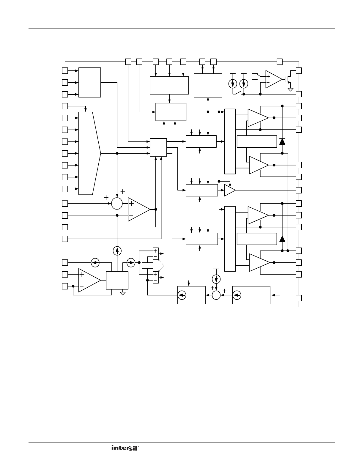
Block Diagram
Σ
ISL62883, ISL62883B
VR_ON
PSI#
DPRSLPVR
RBIAS
VID0
VID1
VID2
VID3
VID4
VID5
VID6
RTN
FB
COMP
VW
IMON
ISUM+
ISUM-
MODE
CONTROL
DAC
AND
SOFT
START
IMON
IDROOP
CURRENT
SENSE
Σ
VIN
VSEN
ISEN1 ISEN3 ISEN2
VIN
CLOCK
VDAC
COMP VW
E/A
2.5X
CURRENT
BALANCE
IBAL
PROTECTION
WOC OC
WOC
CURRENT
COMPARATORS
OC
PGOOD CLK_EN#
PGOOD &
CLK_EN#
LOGIC
FLT
IBAL VIN VDAC
MODULATOR
COMP
COMP
IBAL VIN VDAC
MODULATOR
COMP
IBAL VIN VDAC
MODULATOR
COMP
NUMBER OF
PHASES
GAIN
SELECT
60UA
6µA
54µA
1.24V
DRIVER
SHOOT THROUGH
PROTECTION
PWM CONTROL LOGIC
DRIVER
SHOOT THROUGH
PROTECTION
PWM CONTROL LOGIC
ADJ. OCP
THRESHOLD
1.20V
DRIVER
DRIVER
VDD
COMP
VR_TT#
NTC
BOOT2
UGATE2
PHASE2
LGATE2
VSSP2
PWM3
BOOT1
UGATE1
PHASE1
VCCP
LGATE1
VSSP1
GND
5
FN6891.4
June 21, 2011
ISL62883, ISL62883B
Absolute Maximum Ratings Thermal Information
Supply Voltage, VDD. . . . . . . . . . . . . . . . . . . . . . . . . . . . . . . . . . . -0.3V to +7V
Battery Voltage, VIN . . . . . . . . . . . . . . . . . . . . . . . . . . . . . . . . . . . . . . . . . +28V
Boot Voltage (BOOT). . . . . . . . . . . . . . . . . . . . . . . . . . . . . . . . . . -0.3V to +33V
Boot to Phase Voltage (BOOT-PHASE) . . . . . . . . . . . . . . . . -0.3V to +7V(DC)
. . . . . . . . . . . . . . . . . . . . . . . . . . . . . . . . . . . . . . . . . . . . . -0.3V to +9V(<10ns)
Phase Voltage (PHASE) . . . . . . . . . . . . . . . . -7V (<20ns Pulse Width, 10µJ)
UGATE Voltage (UGATE) . . . . . . . . . . . . . . . . . . . PHASE - 0.3V (DC) to BOOT
. . . . . . . . . . . . . . . . . . . . . . . PHASE-5V (<20ns Pulse Width, 10µJ) to BOOT
LGATE Voltage (LGATE). . . . . . . . . . . . . . . . . . . . . . -0.3V (DC) to VDD + 0.3V
. . . . . . . . . . . . . . . . . . . . . . . -2.5V (<20ns Pulse Width, 5µJ) to VDD + 0.3V
All Other Pins . . . . . . . . . . . . . . . . . . . . . . . . . . . . . . . . . -0.3V to (VDD +0.3V)
Open Drain Outputs, PGOOD, VR_TT#,
CLK_EN# . . . . . . . . . . . . . . . . . . . . . . . . . . . . . . . . . . . . . . . . . -0.3V to +7V
CAUTION: Do not operate at or near the maximum ratings listed for extended periods of time. Exposure to such conditions may adversely impact product
reliability and result in failures not covered by warranty.
NOTES:
4. θ
is measured in free air with the component mounted on a high effective thermal conductivity test board with “direct attach” features. See Tech
JA
Brief TB379.
5. For θ
, the “case temp” location is the center of the exposed metal pad on the package underside.
JC
Thermal Resistance (Typical) θ
40 Ld TQFN Package (Notes 4, 5) . . . . . . . 32 3
48 Ld TQFN Package (Notes 4, 5) . . . . . . . 29 2
Maximum Junction Temperature . . . . . . . . . . . . . . . . . . . . . . . . . . . .+150°C
Maximum Storage Temperature Range . . . . . . . . . . . . . .-65°C to +150°C
Pb-Free Reflow Profile . . . . . . . . . . . . . . . . . . . . . . . . . . . . . . . see link below
http://www.intersil.com/pbfree/Pb-FreeReflow.asp
(°C/W) θJC (°C/W)
JA
Recommended Operating Conditions
Supply Voltage, VDD. . . . . . . . . . . . . . . . . . . . . . . . . . . . . . . . . . . . . . +5V ±5%
Battery Voltage, VIN . . . . . . . . . . . . . . . . . . . . . . . . . . . . . . . . . . +4.5V to 25V
Ambient Temperature
ISL62883HRTZ, ISL62883BHRTZ . . . . . . . . . . . . . . . . .-10°C to +100°C
ISL62883IRTZ. . . . . . . . . . . . . . . . . . . . . . . . . . . . . . . . . .-40°C to +100°C
Junction Temperature
ISL62883HRTZ, ISL62883BHRTZ . . . . . . . . . . . . . . . . .-10°C to +125°C
ISL62883IRTZ. . . . . . . . . . . . . . . . . . . . . . . . . . . . . . . . . .-40°C to +125°C
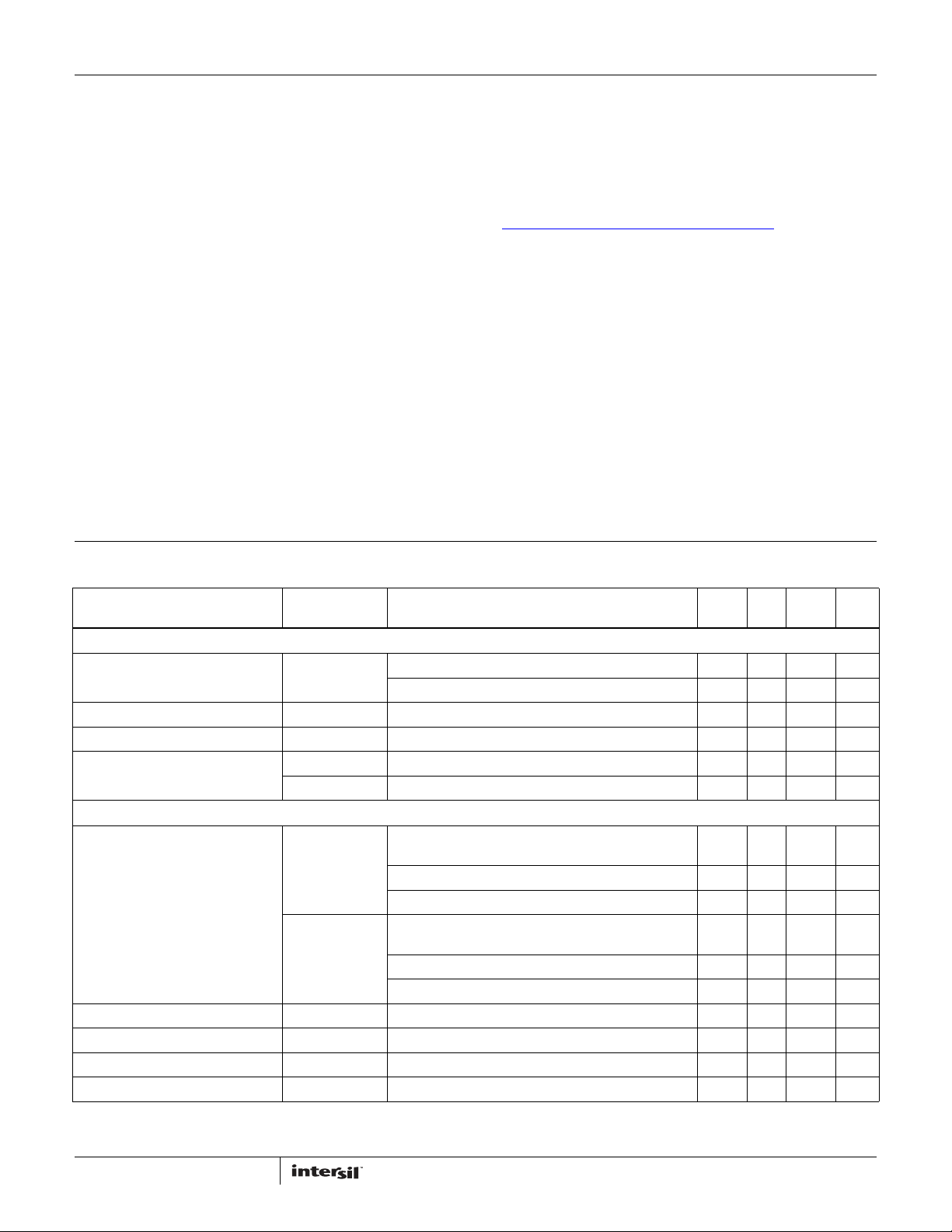
Electrical Specifications Operating Conditions: VDD = 5V, T
limits apply over the operating temperature range, -40°C to +100°C.
PARAMETER SYMBOL TEST CONDITIONS
INPUT POWER SUPPLY
+5V Supply Current I
Battery Supply Current I
V
Input Resistance R
IN
Power-On-Reset Threshold POR
VDD
VIN
VIN
POR
SYSTEM AND REFERENCES
System Accuracy HRTZ
V
BOOT
Maximum Output Voltage V
Minimum Output Voltage V
R
Voltage R
BIAS
%Error (V
IRTZ
%Error (V
CC_CORE(max)
CC_CORE(min)
CC_CORE
CC_CORE
VR_ON = 1V 4 4.6 mA
VR_ON = 0V 1 µA
VR_ON = 0V 1 µA
VR_ON = 1V 900 kΩ
VDD rising 4.35 4.5 V
r
VDD falling 4.00 4.15 V
f
No load; closed loop, active mode range
)
VID = 0.75V to 1.50V
VID = 0.5V to 0.7375V -8 +8 mV
VID = 0.3V to 0.4875V -15 +15 mV
No load; closed loop, active mode range
)
VID = 0.75V to 1.50V
VID = 0.5V to 0.7375V -10 +10 mV
VID = 0.3V to 0.4875V -18 +18 mV
VID = [0000000] 1.500 V
VID = [1100000] 0.300 V
= 147kΩ 1.45 1.47 1.49 V
BIAS
= -40°C to +100°C, fSW = 300kHz, unless otherwise noted. Boldface
A
MIN
(Note 6) TYP
-0.5 +0.5 %
-0.8 +0.8 %
1.0945 1.100 1.1055 V
MAX
(Note 6) UNITS
6
FN6891.4
June 21, 2011
ISL62883, ISL62883B
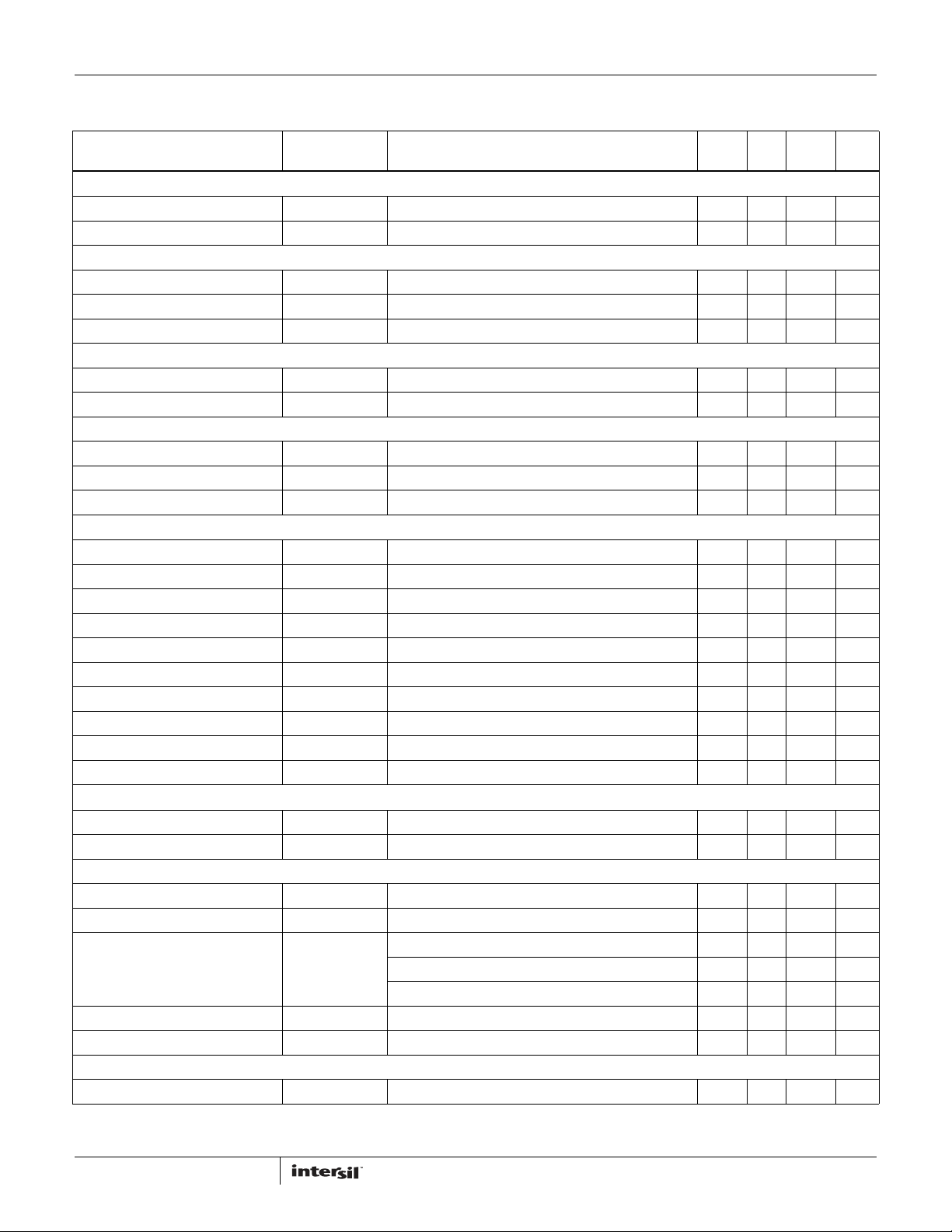
Electrical Specifications Operating Conditions: VDD = 5V, T
= -40°C to +100°C, fSW = 300kHz, unless otherwise noted. Boldface
A
limits apply over the operating temperature range, -40°C to +100°C. (Continued)
PARAMETER SYMBOL TEST CONDITIONS
MIN
(Note 6) TYP
MAX
(Note 6) UNITS
CHANNEL FREQUENCY
Nominal Channel Frequency f
SW(nom)
Rfset = 7kΩ, 3 channel operation, V
= 1V 285 300 315 kHz
COMP
Adjustment Range 200 500 kHz
AMPLIFIERS
Current-Sense Amplifier Input Offset I
Error Amp DC Gain A
v0
Error Amp Gain-Bandwidth Product GBW C
= 0A -0.15 +0.15 mV
FB
90 dB
= 20pF 18 MHz
L
ISEN
Imbalance Voltage Maximum of ISENs - Minimum of ISENs 1 mV
Input Bias Current 20 nA
POWER GOOD AND PROTECTION MONITORS
PGOOD Low Voltage V
PGOOD Leakage Current I
OL
OH
I
= 4mA 0.26 0.4 V
PGOOD
PGOOD = 3.3V -1 1 µA
PGOOD Delay tpgd CLK_EN# LOW to PGOOD HIGH 6.3 7. 6 8.9 ms
GATE DRIVER
UGATE Pull-Up Resistance R
UGATE Source Current I
UGATE Sink Resistance R
UGATE Sink Current I
LGATE Pull-Up Resistance R
LGATE Source Current I
LGATE Sink Resistance R
LGATE Sink Current I
UGATE to LGATE Deadtime t
LGATE to UGAT E De adtim e t
UGPU
UGSRC
UGPD
UGSNK
LGPU
LGSRC
LGPD
LGSNK
UGFLGR
LGFUGR
200mA Source Current 1.0 1.5 Ω
UGATE - PHASE = 2.5V 2.0 A
250mA Sink Current 1.0 1.5 Ω
UGATE - PHASE = 2.5V 2.0 A
250mA Source Current 1.0 1.5 Ω
LGATE - VSSP = 2.5V 2.0 A
250mA Sink Current 0.5 0.9 Ω
LGATE - VSSP = 2.5V 4.0 A
UGATE falling to LGATE rising, no load 23 ns
LGATE falling to UGATE rising, no load 28 ns
BOOTSTRAP DIODE
Forward Voltage V
Reverse Leakage I
F
R
PVCC = 5V, IF = 2mA 0.58 V
VR = 25V 0.2 µA
PROTECTION
Overvoltage Threshold OV
Severe Overvoltage Threshold OV
OC Threshold Offset at Rcomp = Open
Circuit
H
HS
VSEN rising above setpoint for >1ms 150 195 240 mV
VSEN rising for >2µs 1.525 1.55 1.575 V
3-phase configuration, ISUM- pin current 28.4 30.3 32.2 µA
2-phase configuration, ISUM- pin current 18.3 20.2 22.1 µA
1-phase configuration, ISUM- pin current 8.2 10.1 12.0 µA
Current Imbalance Threshold One ISEN above another ISEN for >1.2ms 9 mV
Undervoltage Threshold UV
f
VSEN falling below setpoint for >1.2ms -355 -295 -235 mV
LOGIC THRESHOLDS
VR_ON Input Low V
IL(1.0V)
0.3 V
7
FN6891.4
June 21, 2011
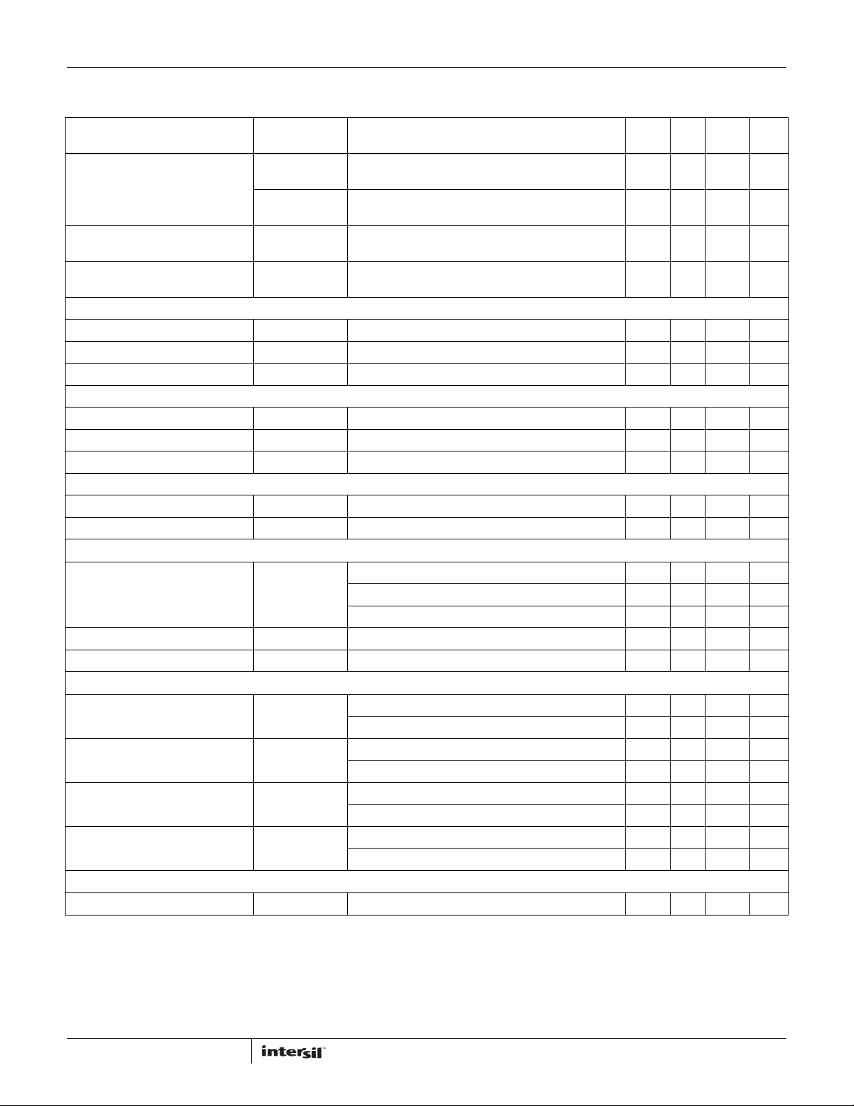
ISL62883, ISL62883B
Electrical Specifications Operating Conditions: VDD = 5V, T
= -40°C to +100°C, fSW = 300kHz, unless otherwise noted. Boldface
A
limits apply over the operating temperature range, -40°C to +100°C. (Continued)
PARAMETER SYMBOL TEST CONDITIONS
VR_ON Input High HRTZ
VID0-VID6, PSI#, and DPRSLPVR Input
Low
VID0-VID6, PSI#, and DPRSLPVR Input
High
PWM
PWM3 Output Low V
PWM3 Output High V
PWM Tri-State Leakage PWM = 2.5V 2 µA
THERMAL MONITOR
NTC Source Current NTC = 1.3V 53 60 67 µA
Over-Temperature Threshold V (NTC) falling 1.18 1.2 1.22 V
VR_TT# Low Output Resistance R
CLK_EN# OUTPUT LEVELS
CLK_EN# Low Output Voltage V
CLK_EN# Leakage Current I
V
IH(1.0V)
IRTZ
V
IH(1.0V)
V
IL(1.0V)
V
IH(1.0V)
OL(5.0V)
OH(5.0V)
TT
OL
OH
Sinking 5mA 1.0 V
Sourcing 5mA 3.5 V
I = 20mA 6.5 9 Ω
I = 4mA 0.26 0.4 V
CLK_EN# = 3.3V -1 1 µA
MIN
(Note 6) TYP
0.7 V
0.75 V
0.7 V
MAX
(Note 6) UNITS
0.3 V
CURRENT MONITOR
IMON Output Current I
IMON Clamp Voltage V
Current Sinking Capability 275 µA
IMON
IMONCLAMP
ISUM- pin current = 20μA 108 120 132 µA
ISUM- pin current = 10μA 51 60 69 µA
ISUM- pin current = 5μA 22 30 37.5 µA
1.1 1.15 V
INPUTS
VR_ON Leakage Current I
VIDx Leakage Current I
PSI# Leakage Current I
DPRSLPVR Leakage Current I
DPRSLPVR
VR_ON
VIDx
PSI#
VR_ON = 0V -1 0µA
VR_ON = 1V 0 1 µA
VIDx = 0V -1 0µA
VIDx = 1V 0.45 1 µA
PSI# = 0V -1 0µA
PSI# = 1V 0.45 1 µA
DPRSLPVR = 0V -1 0µA
DPRSLPVR = 1V 0.45 1 µA
SLEW RATE
Slew Rate (For VID Change) SR 56.5mV/µs
NOTE:
6. Parameters with MIN and/or MAX limits are 100% tested at +25°C, unless otherwise specified. Temperature limits established by characterization
and are not production tested.
8
FN6891.4
June 21, 2011
ISL62883, ISL62883B
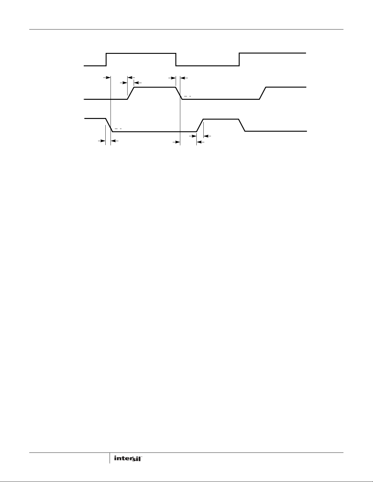
Gate Driver Timing Diagram
PWM
t
LGFUGR
UGATE
t
RU
1V
t
FU
LGATE
1V
t
t
FL
t
UGFLGR
RL
9
FN6891.4
June 21, 2011
ISL62883, ISL62883B
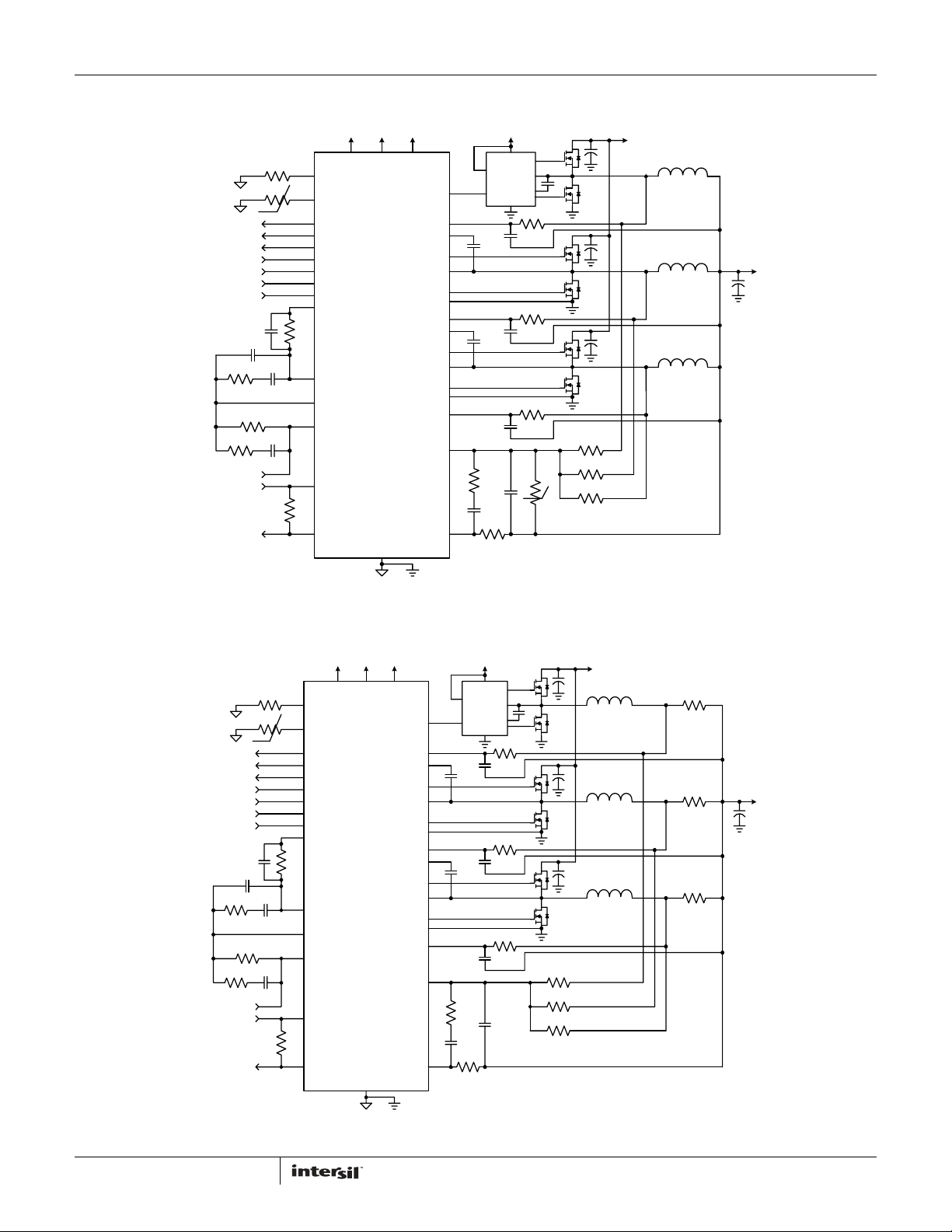
Simplified Application Circuits
V+5 Vin
V+5
VCCP
ISL62883
VSS
VINVDD
PWM3
ISEN3
BOOT2
UGATE2
PHASE2
LGATE2
VSSP2
ISEN2
BOOT1
UGATE1
PHASE1
LGATE1
VSSP1
ISEN1
ISUM+
ISUM-
PGOOD
CLK_EN#
VID<0:6>
PSI#
DPRSLPVR
VR_ON
Rdroop
VCCSENSE
VSSSENSE
IMON
Rbias
Rntc
o
C
Rimon
Rfset
RBIAS
NTC
PGOOD
VR_TT#VR_TT#
CLK_EN#
VIDs
PSI#
DPRSLPVR
VR_ON
VW
COMP
FB
VSEN
RTN
IMON
(Bottom Pad)
Cis
Ris
V+5
FCCM
ISL6208
PWM
Cs3
Cs2
Cs1
Cn
Ri
VCC
GND
UGATE
PHASE
BOOT
LGATE
o
Rs3
Rs2
Rs1
C
Rn
Rsum3
Rsum2
Rsum1
Vin
L3
L2
L1
V
o
PGOOD
CLK_EN#
VID<0:6>
PSI#
DPRSLPVR
VR_ON
Rdroop
VCCSENSE
VSSSENSE
IMON
Rbias
Rntc
o
C
Rimon
FIGURE 1. TYPICAL APPLICATION CIRCUIT USING DCR SENSING
FCCM
PWM
Cs3
Cs2
Cs2
Cn
Ri
V+5
VCC
ISL6208
LGATE
GND
UGATE
PHASE
BOOT
Vin
L3
Rs3
L2
Rs2
L1
Rs1
Rsum3
Rsum2
Rsum1
Rfset
V+5 Vin
RBIAS
NTC
PGOOD
VR_TT#VR_TT#
CLK_EN#
VIDs
PSI#
DPRSLPVR
VR_ON
VW
ISL62883
COMP
FB
VSEN
RTN
IMON
(Bottom Pad)
V+5
VCCP
VSS
VINVDD
PWM3
ISEN3
BOOT2
UGATE2
PHASE2
LGATE2
VSSP2
ISEN2
BOOT1
UGATE1
PHASE1
LGATE1
VSSP1
ISEN1
ISUM+
ISUM-
Ris
Cis
Rsen3
Rsen2
Rsen1
V
o
FIGURE 2. TYPICAL APPLICATION CIRCUIT USING RESISTOR SENSING
10
FN6891.4
June 21, 2011
ISL62883, ISL62883B
Theory of Operation
Multiphase R
MASTER
CLOCK
gmVo
Vcrs1
Crs1
Vcrs2
Crs2
Vcrs3
Crs3
VW
Vcrm
COMP
Master
Clock
Clock1
PWM1
Clock2
PWM2
Clock3
PWM3
FIGURE 4. R
3
™
Modulator
MASTER CLOCK CIRCUIT
VW
COMP
Vcrm
Crm
VW
VW
VW
FIGURE 3. R
MASTER
CLOCK
Phase
Sequencer
SLAVE CIRCUIT 1
Clock1
gm
SLAVE CIRCUIT 2
Clock2
gm
SLAVE CIRCUIT 3
Clock3
gm
3
PWM1
S
Q
R
PWM2
S
Q
R
PWM3
S
Q
R
™ MODULATORCIRCUIT
VW
Vcrs3
Vcrs2 Vcrs1
3
™ MODULATOR OPERATION PRINCIPLES IN
STEADY STATE
Phase1
Phase2
Phase3
Hysteretic
Window
Clock1
Clock2
Clock3
L1
I
L1
L2
I
L2
L3
I
L3
Vo
Co
VW
COMP
Vcrm
Master
Clock
Clock1
PWM1
Clock2
PWM2
Clock3
PWM3
VW
Vcrs1
Vcrs3
Vcrs2
FIGURE 5. R
3
™ MODULATOROPERATION PRINCIPLES IN LOAD
INSERTION RESPONSE
The ISL62883 is a multiphase regulator, which implements Intel™
IMVP-6.5™ protocol. It can be programmed for 1-, 2- or 3-phase
operation for microprocessor core applications. It uses Intersil
patented R
3
™ (Robust Ripple Regulator™) modulator. The R3™
modulator combines the best features of fixed frequency PWM
and hysteretic PWM while eliminating many of their shortcomings.
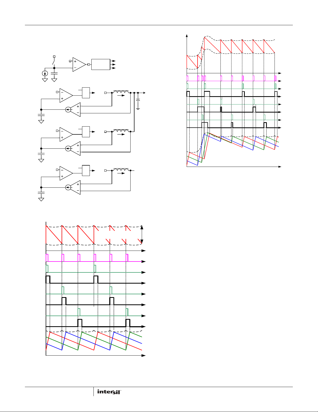
Figure 3 conceptually shows the ISL62883 multiphase R
3
™
modulator circuit, and Figure 4 shows the operation principles.
A current source flows from the VW pin to the COMP pin, creating
a voltage window set by the resistor between the two pins. This
voltage window is called VW window in the following discussion.
Inside the IC, the modulator uses the master clock circuit to
generate the clocks for the slave circuits. The modulator
discharges the ripple capacitor C
to gmVo, where gm is a gain factor. Crm voltage V
with a current source equal
rm
crm
is a
sawtooth waveform traversing between the VW and COMP
voltages. It resets to VW when it hits COMP, and generates a oneshot master clock signal. A phase sequencer distributes the
master clock signal to the slave circuits. If the ISL62883 is in
3-phase mode, the master clock signal will be distributed to the
three phases, and the Clock1~3 signals will be 120° out-ofphase. If the ISL62883 is in 2-phase mode, the master clock
signal will be distributed to Phases 1 and 2, and the Clock1 and
Clock2 signals will be 180° out-of-phase. If the ISL62883 is in
1-phase mode, the master clock signal will be distributed to
Phases 1 only and be the Clock1 signal.
Each slave circuit has its own ripple capacitor C
, whose voltage
rs
mimics the inductor ripple current. A gm amplifier converts the
inductor voltage into a current source to charge and discharge
. The slave circuit turns on its PWM pulse upon receiving the
C
rs
clock signal, and the current source charges Crs. When Crs
11
FN6891.4
June 21, 2011
ISL62883, ISL62883B
voltage V
hits VW, the slave circuit turns off the PWM pulse,
Crs
and the current source discharges Crs.
Since the ISL62883 works with V
, which are large-amplitude
crs
and noise-free synthesized signals, the ISL62883 achieves lower
phase jitter than conventional hysteretic mode and fixed PWM
mode controllers. Unlike conventional hysteretic mode
converters, the ISL62883 has an error amplifier that allows the
controller to maintain a 0.5% output voltage accuracy.
Figure 5 shows the operation principles during load insertion
response. The COMP voltage rises during load insertion,
generating the master clock signal more quickly, so the PWM
pulses turn on earlier, increasing the effective switching
frequency, which allows for higher control loop bandwidth than
conventional fixed frequency PWM controllers. The VW voltage
rises as the COMP voltage rises, making the PWM pulses wider.
During load release response, the COMP voltage falls. It takes
the master clock circuit longer to generate the next master clock
signal so the PWM pulse is held off until needed. The VW voltage
falls as the VW voltage falls, reducing the current PWM pulse
width. This kind of behavior gives the ISL62883 excellent
response speed.
The fact that all the phases share the same VW window voltage
also ensures excellent dynamic current balance among phases.
Diode Emulation and Period Stretching
Phase
UGATE
LGATE
IL
FIGURE 6. DIODE EMULATION
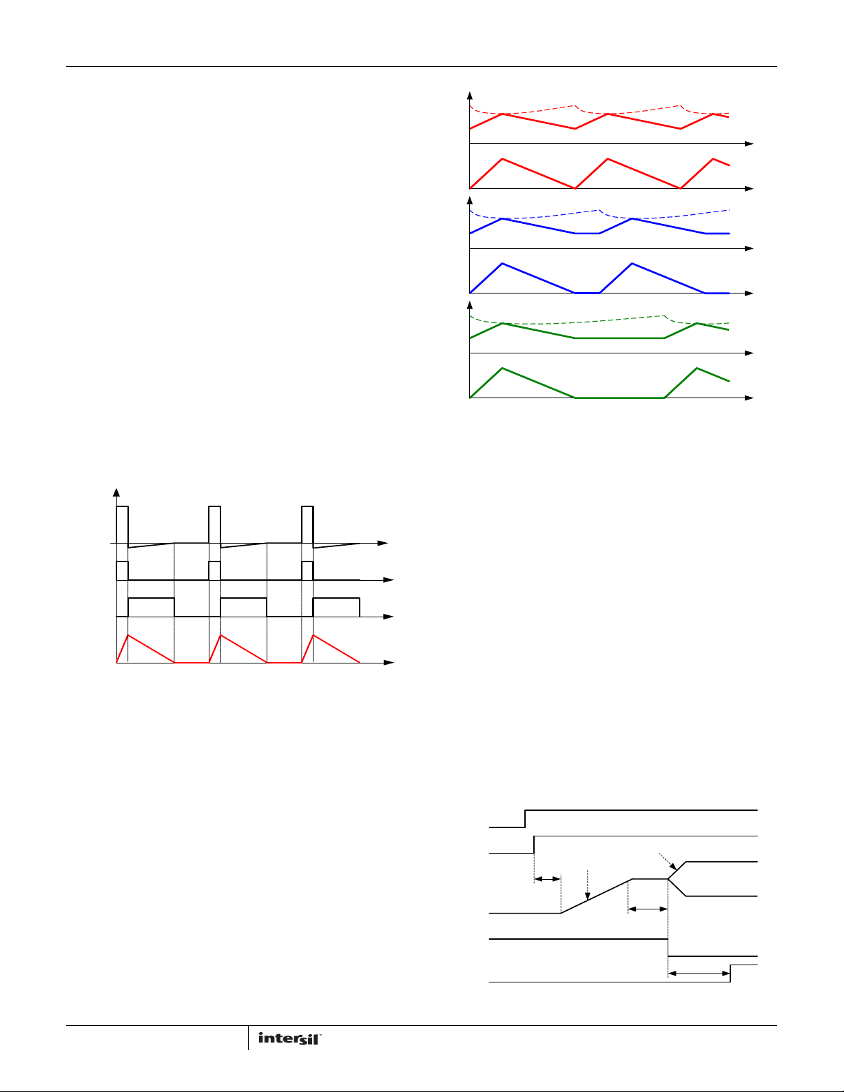
ISL62883 can operate in diode emulation (DE) mode to improve
light load efficiency. In DE mode, the low-side MOSFET conducts
when the current is flowing from source to drain and doesn’t not
allow reverse current, emulating a diode. As Figure 6 shows, when
LGATE is on, the low-side MOSFET carries current, creating
negative voltage on the phase node due to the voltage drop across
the ON-resistance. The ISL62883 monitors the current through
monitoring the phase node voltage. It turns off LGATE when the
phase node voltage reaches zero to prevent the inductor current
from reversing the direction and creating unnecessary power loss.
If the load current is light enough, as Figure 6 shows, the inductor
current will reach and stay at zero before the next phase node
pulse, and the regulator is in discontinuous conduction mode
(DCM). If the load current is heavy enough, the inductor current
will never reach 0A, and the regulator is in CCM although the
controller is in DE mode.
CCM/DCM BOUNDARY
VW
Vcrs
iL
LIGHT DCM
VW
Vcrs
iL
DEEP DCM
Vcrs
iL
VW
FIGURE 7. PERIOD STRETCHING
Figure 7 shows the operation principle in diode emulation mode at
light load. The load gets incrementally lighter in the three cases
from top to bottom. The PWM on-time is determined by the VW
window size, therefore is the same, making the inductor current
triangle the same in the three cases. The ISL62883 clamps the
ripple capacitor voltage V
inductor current. It takes the COMP voltage longer to hit V
in DE mode to make it mimic the
crs
crs
,
naturally stretching the switching period. The inductor current
triangles move further apart from each other such that the
inductor current average value is equal to the load current. The
reduced switching frequency helps increase light load efficiency.
Start-up Timing
With the controller's VDD voltage above the POR threshold, the
start-up sequence begins when VR_ON exceeds the 3.3V logic
high threshold. The ISL62883 uses digital soft start to ramp up
DAC to the boot voltage of 1.1V at about 2.5mV/µs. Once the
output voltage is within 10% of the boot voltage for 13 PWM
cycles (43µs for frequency = 300kHz), CLK_EN# is pulled low and
DAC slews at 5mV/µs to the voltage set by the VID pins. PGOOD
is asser ted high in approximately 7ms. Figure 8 shows the typical
start-up timing. Similar results occur if VR_ON is tied to V
the soft-start sequence starting 120µs after V
crosses the
DD
POR threshold.
VDD
VR_ON
2.5mV/µs
800µs
DAC
CLK_EN#
PGOOD
FIGURE 8. SOFT-START WAVEFORMS
5mV/µs
VBOOT
90%
13 SWITCHING
CYCLES
VID
COMMAND
VOLTAGE
~7ms
DD
, with
12
FN6891.4
June 21, 2011
 Loading...