®
ISL6269B
Data Sheet May 30, 2007
High-Performance Notebook PWM
Controller with Audio-Frequency Clamp
The ISL6269B IC is a Single-Phase Synchronous-Buck
PWM controller featuring Intersil's Robust Ripple Regulator
3
(R
) technology that delivers truly superior dynamic
response to input voltage and output load transients.
Integrated MOSFET drivers and bootstrap diode result in
fewer components and smaller implementation area.
Intersil’s R
3
technology combines the best features of fixedfrequency PWM and hysteretic PWM while eliminating many
of their shortcomings. R
modulator that synthesizes an AC ripple voltage signal V
3
technology employs an innovative
,
R
analogous to the output inductor ripple current. The AC signal
V
enters a window comparator where the lower threshold is
R
the error amplifier output V
programmable voltage reference V
of the PWM signal. The voltage reference V
, and the upper threshold is a
COMP
resulting in generation
W,
sets the steady-
W
state PWM frequency. Both edges of the PWM can be
modulated in response to input voltage transients and output
load transients, much faster than conventional fixedfrequency PWM controllers. Unlike a conventional hysteretic
converter, the ISL6269B h as an error amplifier that provides
±1% voltage regulation at the FB pin.
The ISL6269B has a 1.5ms digital soft-start and can be
started into a pre-biased output voltage. A resistor divider is
used to program the output voltage setpoint. The ISL6269B
can be configured to operate in continuous-conductionmode (CCM) or diode-emulation-mode (DEM), which
improves light-load efficiency. In CCM the controller always
operates as a synchronous rectifier however, when DEM is
enabled the low-side MOSFET is permitted to stay off,
blocking negative current flow into the low-side MOSFET
from the output inductor.
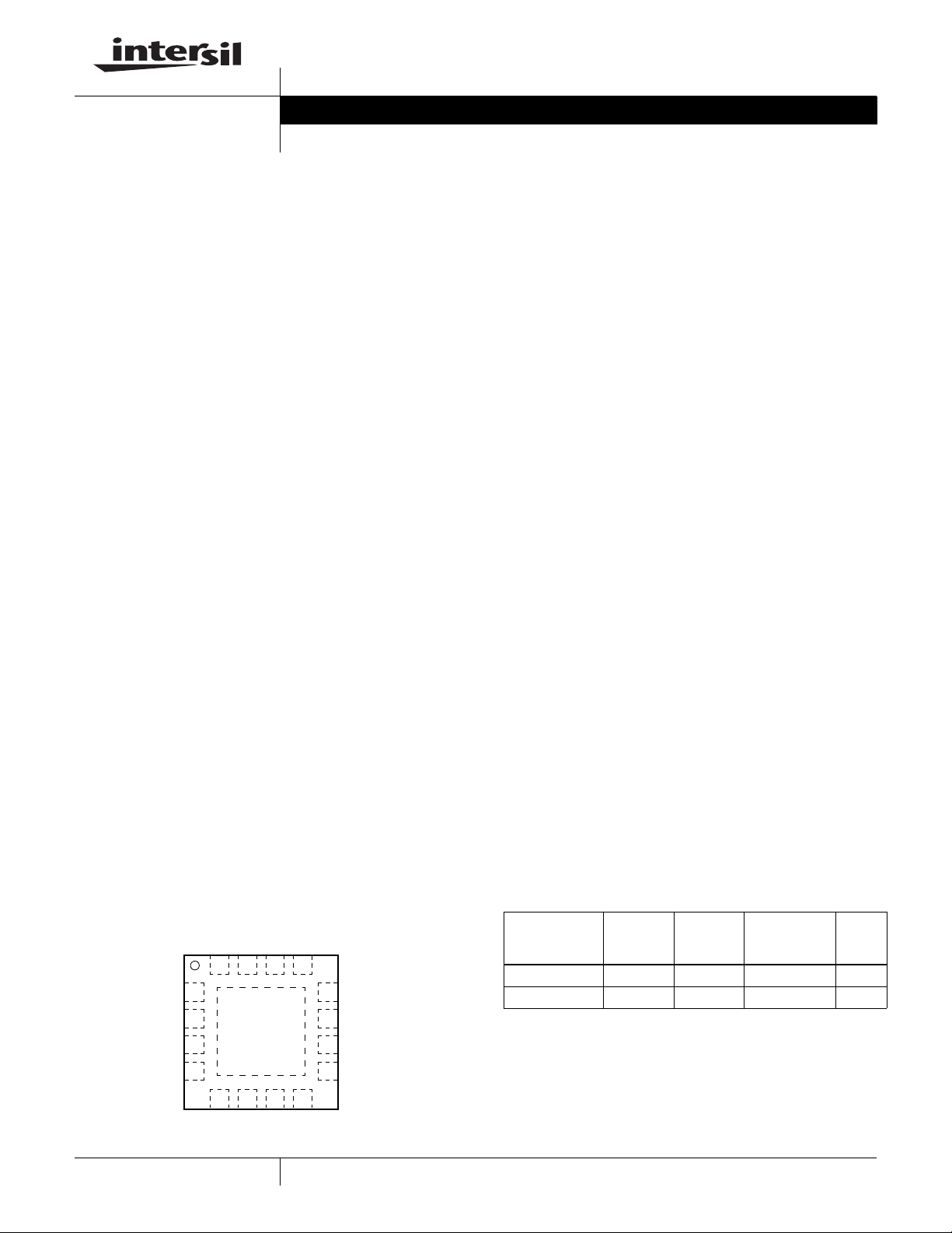
Pinout
ISL6269B
(16 LD 4x4 QFN)
TOP VIEW
FSET
BOOT
12
11
10
9
VO
PVCC
LG
PGND
ISEN
VIN
VCC
FCCM
EN
1
2
3
4
PGOODUGPHASE
1516 14 13
GND
6578
FB
COMP
FN6280.2
Features
• High performance R3 technology
• Fast transient response
• ±1% regulation accuracy: -10°C to +100°C and
-40° to +100°C
• Wide input voltage range: +5.0V to +25.0V
• Output voltage range: +0.6V to +3.3V
• Wide output load range: 0A to 25A
• Selectable diode emulation mode for increased light load
efficiency
• Programmable PWM frequency: 200kHz to 600kHz
• Pre-biased output start-up capability
• Integrated MOSFET drivers and bootstrap diode
• Internal digital soft-start
• Power good monitor
• PWM minimum frequency above audible spectrum
• Fault protection
- Undervoltage protection
- Soft crowbar overvoltage protection
- Low-side MOSFET r
overcurrent protection
DS(ON)
- Over-temperature protection
- Fault identification by PGOOD pull down resi stance
• Pb-free plus anneal available (RoHS compliant)
Applications
• PCI express graphical processing unit
• Auxiliary power rail
•VRM
• Network adapter
Ordering Information
TEMP
PART NUMBER
(Note)
ISL6269BCRZ* 62 69BCRZ -10 to +100 16 Ld 4x4 QFN L16.4x4
ISL6269BIRZ* 62 69BIRZ -40 to +100 16 Ld 4x4 QFN L16.4x4
*Add “-T” suffix for tape and reel.
NOTE: Intersil Pb-free plus anneal products employ special Pb-free
material sets; molding compounds/die attach materials and 100%
matte tin plate termination finish, which are RoHS compliant and
compatible with both SnPb and Pb-free soldering operations. Intersil
Pb-free products are MSL classified at Pb-free peak reflow
temperatures that meet or exceed the Pb-free requirements of
IPC/JEDEC J STD-020.
PART
MARKING
RANGE
(°C)
PACKAGE
(Pb-free)
PKG.
DWG. #
1
CAUTION: These devices are sensitive to electrostatic discharge; follow proper IC Handling Procedures.
1-888-INTERSIL or 1-888-468-3774
| Intersil (and design) is a registered trademark of Intersil Americas Inc.
Copyright Intersil Americas Inc. 2006, 2007. All Rights Reserved
All other trademarks mentioned are the property of their respective owners.
Block Diagram
VIN
GND
VCC
2
EN
PACKAGE BOTTOM
V
REF
−
OVP
+
−
UVP
+
+
+
gmV
−
gmV
−
PWM FREQUENCY
CONTROL
−
+
IN
V
W
−
+
R
PWM
V
R
O
+
C
R
V
COMP
−
+
Q
S
−
VO
FSET
ISL6269B
BOOT
+
EA
FB
−
EA
POR
DRIVER
DIGITAL SOFT-START
UG
COMP
ISEN
PGOOD
May 30, 2007
FN6280.2
−
I
OC
OCP
+
30Ω
90Ω
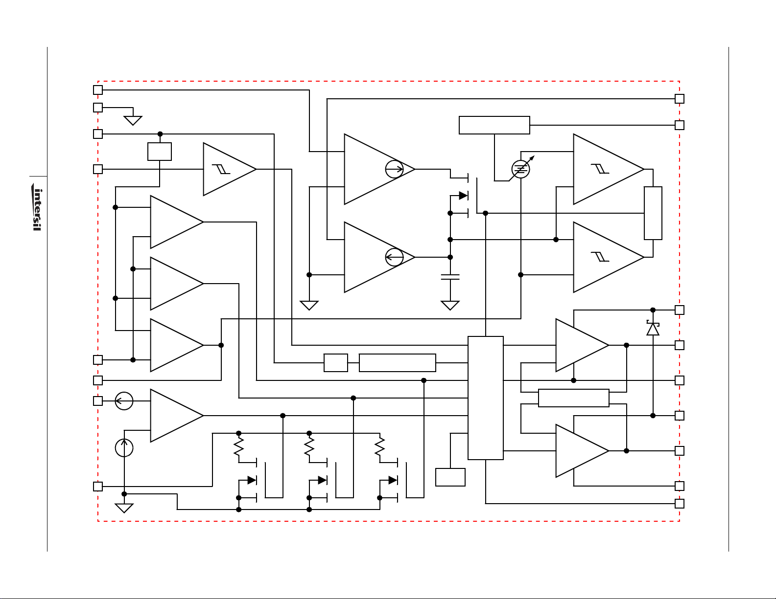
FIGURE 1. SCHEMATIC BLOCK DIAGRAM
60Ω
150°OT
PWM CONTROL
SHOOT THROUGH
PROTECTION
DRIVER
PHASE
PVCC
LG
PGND
FCCM
Typical Application
5V
R
VCC
R
PGOOD
PGOOD
PVCC
ISL6269B
ISL6269B
VIN
UG
V
IN
5V TO 25V
C
IN
Q
HIGH_SIDE
C
PVCC
R
COMP
C
VCC
C
COMP1
VCC
GND
FCCM
EN
COMP
BOOT
PHASE
ISEN
LG
PGND
C
BOOT
R
SEN
L
OUT
Q
LOW_SIDE
V
OUT
0.6V TO 3.3V
C
OUT
C
COMP2
R
BOTTOM
R
FB
VO
TOP
FSET
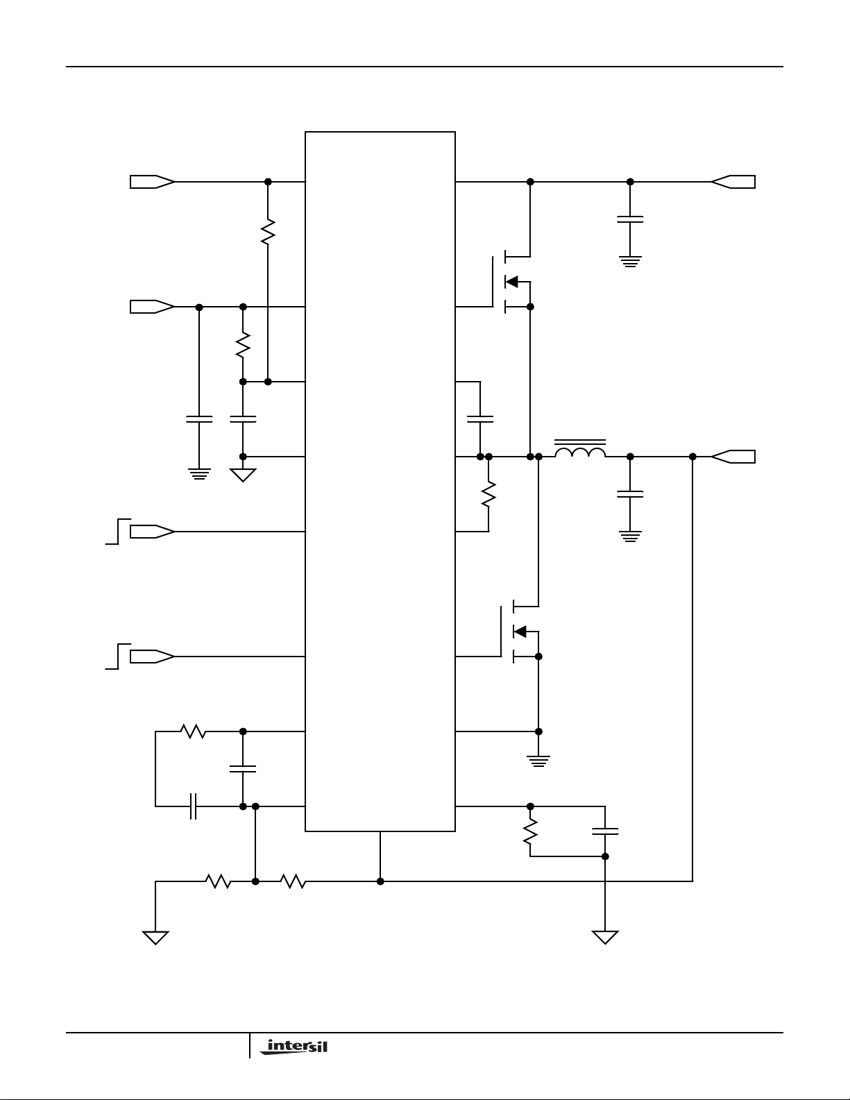
FIGURE 2. ISL6269B TYPICAL APPLICATION SCHEMATIC
3
R
FSET
C
FSET
FN6280.2
May 30, 2007
ISL6269B
Absolute Voltage Ratings
ISEN, VIN to GND . . . . . . . . . . . . . . . . . . . . . . . . . . . .-0.3V to +28V
VCC, PGOOD to GND. . . . . . . . . . . . . . . . . . . . . . . . -0.3V to +7.0V
PVCC to PGND . . . . . . . . . . . . . . . . . . . . . . . . . . . . . -0.3V to +7.0V
GND to PGND . . . . . . . . . . . . . . . . . . . . . . . . . . . . . . -0.3V to +0.3V
EN, FCCM . . . . . . . . . . . . . . . . . . . . . . . . -0.3V to GND, VCC +3.3V
VO, FB, COMP, FSET . . . . . . . . . . . . . . . -0.3V to GND, VCC +0.3V
PHASE to GND (DC). . . . . . . . . . . . . . . . . . . . . . . . . .-0.3V to +28V
(<100ns Pulse Width, 10μJ). . . . . . . . . . . . . . . . . . . . . . . . . -5.0V
BOOT to GND, or PGND. . . . . . . . . . . . . . . . . . . . . . .-0.3V to +33V
BOOT to PHASE . . . . . . . . . . . . . . . . . . . . . . . . . . . . . .-0.3V to +7V
UG (DC). . . . . . . . . . . . . . . . . . . . . . .-0.3V to PHASE, BOOT +0.3V
(<200ns Pulse Width, 20μJ) . . . . . . . . . . . . . . . . . . . . . . . . -4.0V
LG (DC) . . . . . . . . . . . . . . . . . . . . . . . .-0.3V to PGND, PVCC +0.3V
(<100ns Pulse Width, 4μJ). . . . . . . . . . . . . . . . . . . . . . . . . . -2.0V
Thermal Information
Thermal Resistance (Typical, Notes 1, 2) θJA (°C/W) θJC (°C/W)
QFN Package. . . . . . . . . . . . . . . . . . . . 48 11.5
Junction Temperature Range. . . . . . . . . . . . . . . . . .-55°C to +150°C
Operating Temperature Range . . . . . . . . . . . . . . . . . . . . . . . . . . . . .
ISL6269BCRZ . . . . . . . . . . . . . . . . . . . . . . . . . . .-10°C to +100°C
ISL6269BIRZ . . . . . . . . . . . . . . . . . . . . . . . . . . . .-40°C to +100°C
Storage Temperature. . . . . . . . . . . . . . . . . . . . . . . .-65°C to +150°C
Pb-free reflow profile . . . . . . . . . . . . . . . . . . . . . . . . . .see link below
http://www.intersil.com/pbfree/Pb-FreeReflow.asp
Recommended Operating Conditions
Ambient Temperature Range. . . . . . . . . . . . . . . . . . . . . . . . . . . . . . .
ISL6269BCRZ . . . . . . . . . . . . . . . . . . . . . . . . . . .-10°C to +100°C
ISL6269BIRZ . . . . . . . . . . . . . . . . . . . . . . . . . . . .-40°C to +100°C
Supply Voltage (VIN to GND) . . . . . . . . . . . . . . . . . . . . . . 5V to 25V
VCC to GND . . . . . . . . . . . . . . . . . . . . . . . . . . . . . . . . . . . . .5V ±5%
PVCC to PGND . . . . . . . . . . . . . . . . . . . . . . . . . . . . . . . . . . .5V ±5%
CAUTION: Stress above those listed in “Absolute Maximum Ratings” may cause permanent damage to the device. This is a stress only rating and operation of the
device at these or any other conditions above those indicated in the operational section of this specification is not implied.
NOTES:
is measured in free air with the component mounted on a high effective thermal conductivity test board with “direct attach” features. See
1. θ
JA
Tech Brief TB379.
2. For θ
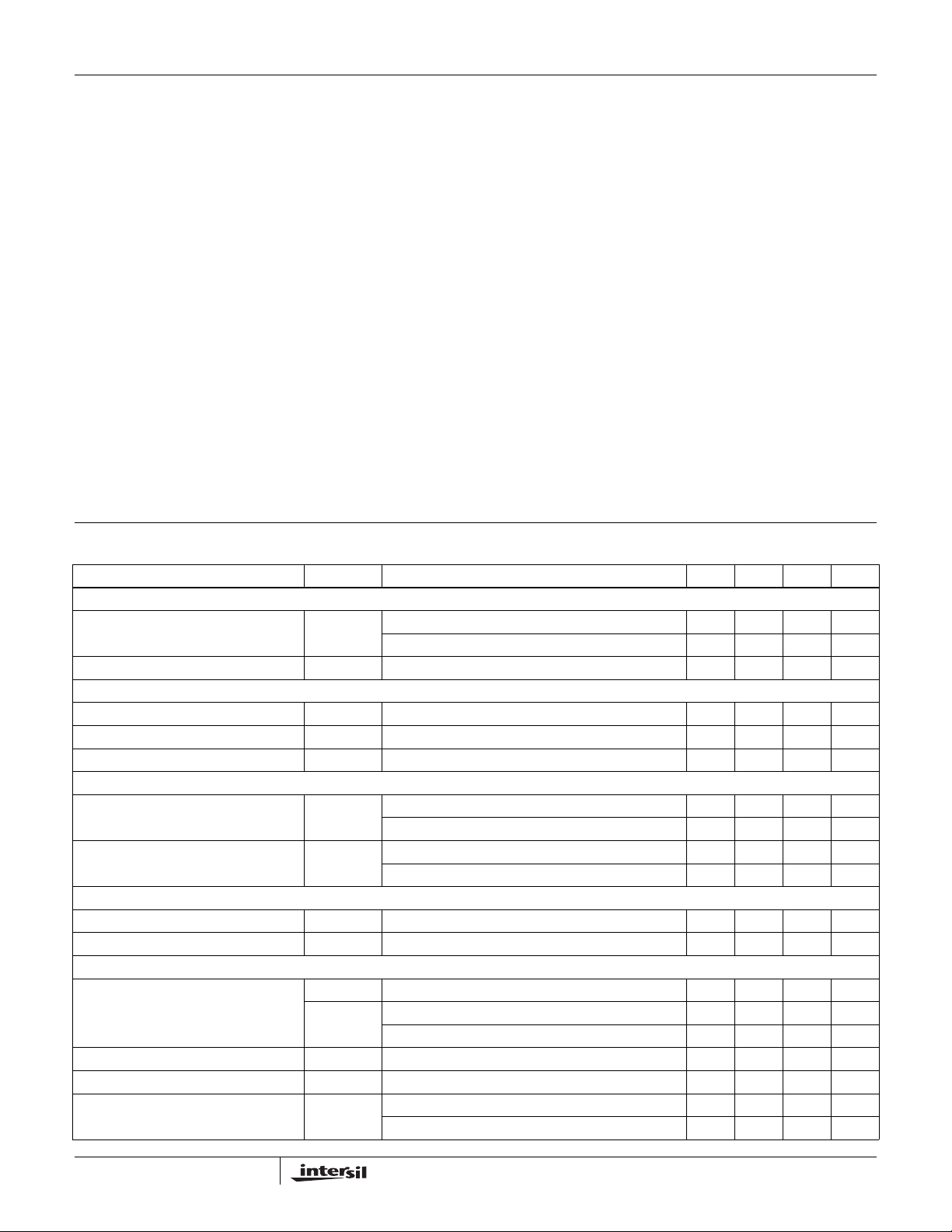
Electrical Specifications These specifications apply for T
, the “case temp” location is the center of the exposed metal pad on the package underside.
JC
= -40°C to +100°C, unless otherwise stated.
All typical specifications T
A
= +25°C, VCC = 5V, PVCC = 5V, VIN = 15V
A
PARAMETER SYMBOL TEST CONDITIONS MIN TYP MAX UNIT
VIN
VIN Input Bias Current
VIN Shutdown Current I
I
VIN
VIN_SHDN
EN = 5V, VIN = 5V - 6.5 10 μA
EN = 5V, VIN = 25V - 26 35 μA
EN = GND, VIN = 25V - 0.1 1.0 μA
VCC and PVCC
VCC Input Bias Current I
VCC Shutdown Current I
PVCC Shutdown Current I
VCC_SHDN
PVCC_SHDN
VCC
EN = 5V , FCCM = GND, FB = 0.65V - 1.7 2.5 mA
EN = GND, VCC = 5V - 0.1 1.0 μA
EN = GND, PVCC = 5V - 0.1 1.0 μA
VCC POR THRESHOLD
Rising VCC POR Threshold Voltage V
VCC_THRTA
= -10°C to +100°C 4.35 4.45 4.55 V
4.33 4.45 4.55 V
Falling VCC POR Threshold Voltage
V
VCC_THFTA
= -10°C to +100°C 4.10 4.20 4.30 V
4.08 4.20 4.30 V
REGULATION
Reference Voltage V
REF
- 0.6 - V
Regulation Accuracy FB connected to COMP -1 - +1 %
PWM
Frequency Range f
SW
f
AUDIO
FCCM = 5V 200 - 600 kHz
FCCM = GND, TA = -10°C to +100°C 19 28 - kHz
FCCM = GND 18 28 - kHz
Frequency-Set Accuracy f
VO Range V
VO Input Leakage I
VO
VO
= 300kHz -12 - +12 %
SW
0.60 - 3.30 V
VO = 0.60V - 1.3 - μA
VO = 3.30V - 7.0 - μA
4
FN6280.2
May 30, 2007
ISL6269B
Electrical Specifications These specifications apply for T
All typical specifications T
= -40°C to +100°C, unless otherwise stated.
A
= +25°C, VCC = 5V, PVCC = 5V, VIN = 15V (Continued)
A
PARAMETER SYMBOL TEST CONDITIONS MIN TYP MAX UNIT
ERROR AMPLIFIER
FB Input Bias Current I
COMP Source Current I
COMP Sink Current I
COMP High Clamp Voltage V
COMP Low Clamp Voltage V
COMP_SRC
COMP_SNK
COMP_HC
COMP_LC
FB
FB = 0.60V -0.5 - +0.5 μA
FB = 0.40V, COMP = 3.20V - 2.5 - mA
FB = 0.80V, COMP = 0.30V - 0.3 - mA
FB = 0.40V, Sink 50μA 3.10 3.40 3.65 V
FB = 0.80V, Source 50μA 0.09 0.15 0.21 V
POWER GOOD
PGOOD Pull-down Impedance R
PG_SS
PGOOD = 5mA Sink, TA = -10°C to +100°C 75 95 125 Ω
PGOOD = 5mA Sink 67 95 125 Ω
R
PG_UV
PGOOD = 5mA Sink, TA = -10°C to +100°C 75 95 125 Ω
PGOOD = 5mA Sink 67 95 125 Ω
R
PG_OV
PGOOD = 5mA Sink, TA = -10°C to +100°C 50 63 85 Ω
PGOOD = 5mA Sink 45 63 85 Ω
R
PG_OC
PGOOD = 5mA Sink, TA = -10°C to +100°C 25 32 45 Ω
PGOOD = 5mA Sink 22 32 45 Ω
PGOOD Leakage Current I
PGOOD
PGOOD = 5V - 0.1 1.0 μA
PGOOD Maximum Sink Current (Note 3) - 5.0 - mA
PGOOD Soft-Start Delay t
SS
EN High to PGOOD High, TA = -10°C to +100°C 2.20 2.75 3.30 ms
EN High to PGOOD High 2.20 2.75 3.50 ms
GATE DRIVER
UG Pull-Up Resistance R
UG Source Current (Note 3) I
UG Sink Resistance R
UG Sink Current (Note 3) I
LG Pull-Up Resistance R
LG Source Current (Note 3) I
LG Sink Resistance R
LG Sink Current (Note 3) I
UG to LG Deadtime t
LG to UG Deadtime t
UGPU
UGSRC
UGPD
UGSNK
LGPU
LGSRC
LGPD
LGSNK
UGFLGR
LGFUGR
200mA Source Current - 1.0 1.5 Ω
UG - PHASE = 2.5V - 2.0 - A
250mA Sink Current - 1.0 1.5 Ω
UG - PHASE = 2.5V - 2.0 - A
250mA Source Current - 1.0 1.5 Ω
LG - PGND = 2.5V - 2.0 - A
250mA Sink Current - 0.5 0.9 Ω
LG - PGND = 2.5V - 4.0 - A
UG falling to LG rising, no load - 21 - ns
LG falling to UG rising, no load - 14 - ns
BOOTSTRAP DIODE
Forward Voltage V
Reverse Leakage I
PVCC = 5V, IF = 2mA - 0.58 - V
F
VR = 25V - 0.2 - μA
R
CONTROL INPUTS
EN High Threshold V
EN Low Threshold V
FCCM High Threshold V
FCCM Low Threshold V
FCCMTHR
FCCMTHF
EN Leakage I
FCCM Leakage I
ENTHR
ENTHF
ENL
I
ENH
FCCML
I
FCCMH
EN = 0V - 0.1 1.0 μA
EN = 5.0V - 0.1 1.0 μA
FCCM = 0V - 0.1 1.0 μA
FCCM = 5.0V - 2.0 - μA
2.0 --V
--1.0 V
2.0 --V
--1.0 V
5
FN6280.2
May 30, 2007
 Loading...