

Intersil ISL6262A Datasheet
®
ISL6262A
Data Sheet December 23, 2008
Two-Phase Core Controller
(Santa Rosa, IMVP-6+)
The ISL6262A is a two-phase buck converter regulator
implementing Intel® IMVP-6+ protocol with embedded gate
drivers. The two-phase buck converter uses two interleaved
channels to effectively double the output voltage ripple
frequency, and thereby reduce output voltage ripple
amplitude with fewer components; lower component cost;
reduced power dissipation; and smaller real estate area.
The heart of the ISL6262A is the patented R
Intersil’s Robust Ripple Regulator modulator. Compared with
the traditional multiphase buck regulator, the R
T echnology™ has the fastest transient response. This is due
to the R
3
modulator commanding variable switching
frequency during a load transient.
Intel® Mobile Voltage Positioning (IMVP) is a smart voltage
regulation technology, which ef fectively reduces power
dissipation in Intel® Pentium processors. T o boost battery
life, the ISL6262A supports DPRSLPVR (deeper sleep),
DPRSTP# and PSI# functions, and maximizes the efficiency
via automatically enabling different phase operation modes.
At heavy load operation of the active mode, the regulator
commands the two phase continuous conduction mode
(CCM) operation. While the PSI# is asserted with medium
load in active mode, the ISL6262A smoothly disables one
phase and operates in one-phase CCM. When the CPU
enters deeper sleep mode, the ISL6262A enables diode
emulation to maximize the efficiency at light load.
For better system power management of the portable
computer, the ISL6262A also provides a CPU power monitor
output. The analog output at the power monitor pin can be
fed into an A/D converter to report instantaneous or average
CPU power.
A 7-bit digital-to-analog converter (DAC) allows dynamic
adjustment of the core output voltage from 0.300V to 1.500V .
A 0.5% system accuracy of the core output voltage
over-temperature is achieved by the ISL6262A.
A unity-gain differential amplifier is provided for remote CPU
die sensing. This allows the voltage on the CPU die to be
accurately measured and regulated per Intel® IMVP-6+
specifications. Current sensing can be realized using either
lossless inductor DCR sensing, or precision resistor sensing.
A single NTC thermistor network thermally compensates the
gain and the time constant of the DCR variations.
3
Technology™,
3
FN6343.1
Features
• Precision Two/One-phase CORE Voltage Regulator
- 0.5% System Accuracy Over-Temperature
- Enhanced Load Line Accuracy
• Internal Gate Driver with 2A Driving Capability
• Dynamic Phase Adding/Dropping
• Microprocessor Voltage Identification Input
- 7-Bit VID Input
- 0.300V to 1.500V in 12.5mV Steps
- Support VID Change On-the-Fly
• Multiple Current Sensing Schemes Supported
- Lossless Inductor DCR Current Sensing
- Precision Resistive Current Sensing
• CPU Power Monitor
• Thermal Monitor
• User Programmable Switching Frequency
• Differential Remote CPU Die Voltage Sensing
• Static and Dynamic Current Sharing
• Overvoltage, Undervoltage, and Overcurrent Protection
• Pb-Free (RoHS Compliant)
Ordering Information
TEMP.
PART NUMBER
(Note)
ISL6262ACRZ ISL6262 ACRZ -10 to +100 48 Ld 7x7 QFN L48.7x7
ISL6262ACRZ-T* ISL6262 ACRZ -10 to +100 48 Ld 7x7 QFN L48.7x7
ISL6262AIRZ ISL6262 AIRZ -40 to +100 48 Ld 7x7 QFN L48.7x7
ISL6262AIRZ-T* ISL6262 AIRZ -40 to +100 48 Ld 7x7 QFN L48.7x7
*Please refer to TB347 for details on reel specifications.
NOTE: These Intersil Pb-free plastic packaged products employ special
Pb-free material sets, molding compounds/die attach materials, and
100% matte tin plate plus anneal (e3 termination finish, which is RoHS
compliant and compatible with both SnPb and Pb-free soldering
operations). Intersil Pb-free products are MSL classified at Pb-free peak
reflow temperatures that meet or exceed the Pb-free requirements of
IPC/JEDEC J STD-020.
PART
MARKING
RANGE
(°C)
PACKAGE
(Pb-Free)
PKG.
DWG. #
1
Intel® is a registered trademark of Intel Corporation. All other trademarks mentioned are the property of their respective owners.
Copyright Intersil Americas Inc. 2008. All Rights Reserved. R
CAUTION: These devices are sensitive to electrostatic discharge; follow proper IC Handling Procedures.
1-888-INTERSIL or 1-888-468-3774
| Intersil (and design) is a registered trademark of Intersil Americas Inc.
3
Technology™ is a trademark of Intersil Americas Inc.
Pinout
ISL6262A
ISL6262A
(48 LD 7x7 QFN)
TOP VIEW
3V3
CLK_EN#
DPRSTP#
DPRSLPVR
VR_ON
VID6
VID5
VID4
VID3
VID2
VID1
48 47 46 45 44 43 42 41 40 39 38 37
VID0
PGOOD
PSI#
PMON
RBIAS
VR_TT#
NTC
SOFT
OCSET
VW
COMP
FB
FB2
1
2
3
4
5
6
7
8
9
10
11
12
13 14 15 16 17 18 19 20 21 22 23 24
RTN
VSEN
VDIFF
DROOP
GND PAD
(BOTTOM)
VO
DFB
VSUM
VIN
GND
36
BOOT1
35
UGATE1
34
PHASE1
33
PGND1
LGATE1
32
31
PVCC
30
LGATE2
29
PGND2
PHASE2
28
UGATE2
27
BOOT2
26
NC
25
VDD
ISEN2
ISEN1
2
FN6343.1
December 23, 2008
ISL6262A
Absolute Maximum Ratings Thermal Information
Supply Voltage, VDD. . . . . . . . . . . . . . . . . . . . . . . . . . . -0.3 to +7V
Battery Voltage, VIN. . . . . . . . . . . . . . . . . . . . . . . . . . . . . . . . . +28V
Boot Voltage (BOOT). . . . . . . . . . . . . . . . . . . . . . . . . .-0.3V to +33V
Boot to Phase Voltage (BOOT to PHASE . . . . . . -0.3V to +7V (DC)
-0.3V to +9V (<10ns)
Phase Voltage (PHASE) . . . . . . . . . -7V (<20nS Pulse Width, 10µJ)
UGATE Voltage (UGATE) . . . . . . . . . . PHASE -0.3V (DC) to BOOT
. . . . . . . . . . . . . PHASE-5V (<20nS Pulse Width, 10µJ) to BOOT
LGATE Voltage (LGATE) . . . . . . . . . . . . -0.3V (DC) to (VDD +0.3V)
. . . . . . . . . . . . . .-2.5V (<20nS Pulse Width, 5µJ) to (VDD +0.3V)
All Other Pins. . . . . . . . . . . . . . . . . . . . . . . . . .-0.3V to (VDD +0.3V)
Open Drain Outputs, PGOOD, VR_TT# . . . . . . . . . . . . -0.3 to +7V
CAUTION: Do not operate at or near the maximum ratings listed for extended periods of time. Exposure to such conditions may adversely impact product reliability and
result in failures not covered by warranty.
NOTES:
is measured in free air with the component mounted on a high effective thermal conductivity test board with “direct attach” features. See
1. θ
JA
Tech Brief TB379.
2. For θ
, the “case temp” location is the center of the exposed metal pad on the package underside.
JC
Thermal Resistance (Typical)
θJA
°C/W θJC°C/W
QFN Package (Notes 1, 2). . . . . . . . . . 29 4.5
Maximum Storage Temperature Range. . . . . . . . . -65°C to +150°C
Maximum Junction Temperature . . . . . . . . . . . . . . . . . . . . . +150°C
Pb-free reflow profile . . . . . . . . . . . . . . . . . . . . . . . . . .see link below
http://www.intersil.com/pbfree/Pb-FreeReflow.asp
Recommended Operating Conditions
Supply Voltage, VDD. . . . . . . . . . . . . . . . . . . . . . . . . . . . . +5V ±5%
Battery Voltage, VIN . . . . . . . . . . . . . . . . . . . . . . . . . . . +5V to 25V
Ambient Temperature
Commercial . . . . . . . . . . . . . . . . . . . . . . . . . . . . -10°C to +100°C
Industrial. . . . . . . . . . . . . . . . . . . . . . . . . . . . . . . -40°C to +100°C
Junction Temperature
Commercial . . . . . . . . . . . . . . . . . . . . . . . . . . . . -10°C to +125°C
Industrial. . . . . . . . . . . . . . . . . . . . . . . . . . . . . . . -40°C to +125°C
Electrical Specifications V
= 5V, TA = -40°C to +100°C, unless otherwise specified. Parameters with MIN and/or MAX limits are 100%
DD
tested at +25°C, unless otherwise specified. Temperature limits established by characterization and are not
production tested.
PARAMETER SYMBOL TEST CONDITIONS MIN TYP MAX UNITS
INPUT POWER SUPPLY
+5V Supply Current I
VDD
VR_ON = 3.3V 3.6 4.1 mA
VR_ON = 0V 1 µA
+3.3V Supply Current I
Battery Supply Current at VIN pin I
3V3
VIN
POR (Power-On Reset) Threshold POR
POR
No load on CLK_EN# 1 µA
VR_ON = 0V, VIN = 25V 1 µA
VDD Rising 4.35 4.5 V
r
VDD Falling 4.0 4.15 V
f
SYSTEM AND REFERENCES
System Accuracy %Error
(V
CC_CORE
ISL6262ACRZ
No load, closed loop, active mode,
T
)
= 0°C to +100°C, VID = 0.75 to 1.5V -0.5 0.5 %
A
VID = 0.5 to 0.7375V -8 8 mV
VID = 0.3 to 0.4875V -15 15 mV
System Accuracy %Error
(V
CC_CORE
ISL6262AIRZ
No load, closed loop, active mode,
T
)
= -40°C to +100°C, VID = 0.75 to 1.5V
A
-0.8 0.8 %
VID = 0.5 to 0.7375V -10 10
VID = 0.3 to 0.4875V 18 18 mV
Droop Amplifier Offset 0.3 0.3
Voltage R
R
BIAS
Boot Voltage V
Maximum Output Voltage V
V
RBIAS
BOOT
CC_CORE
(max)
CC_CORE
R
= 147kΩ 1.45 1.47 1.49 V
RBIAS
1.188 1.2 1.212 V
VID = [0000000] 1.5 V
VID = [1100000] 0.3 V
(min)
VID Off State VID = [1111111] 0 V
3
FN6343.1
December 23, 2008
ISL6262A
Electrical Specifications V
= 5V, TA = -40°C to +100°C, unless otherwise specified. Parameters with MIN and/or MAX limits are 100%
DD
tested at +25°C, unless otherwise specified. Temperature limits established by characterization and are not
production tested. (Continued)
PARAMETER SYMBOL TEST CONDITIONS MIN TYP MAX UNITS
CHANNEL FREQUENCY
R
Nominal Channel Frequency f
SW
= 6.9kΩ, 2 channel operation,
FSET
V
= 2V
COMP
285 300 315 kHz
Adjustment Range 100 500 kHz
AMPLIFIERS
Droop Amplifier Offset -0.3 0.3 mV
Error Amp DC Gain A
V0
Error Amp Gain-Bandwidth Product GBW C
Error Amp Slew Rate SR C
FB Input Current I
IN(FB)
= 20pF 18 MHz
L
= 20pF 5 V/µs
L
90 dB
10 150 nA
ISEN
Imbalance Voltage 2mV
Input Bias Current 20 nA
SOFT-START CURRENT
Soft-Start Current I
Soft Geyserville Current I
Soft Deeper Sleep Entry Current I
Soft Deeper Sleep Exit Current I
Soft Deeper Sleep Exit Current I
SS
GV
C4
C4EA
C4EB
|SOFT - REF|>100mV ±180 ±205 ±230 µA
DPRSLPVR = 3.3V -47 -42 -37 µA
DPRSLPVR = 3.3V 37 42 47 µA
DPRSLPVR = 0V 180 205 230 µA
-47 -42 -37 µA
GATE DRIVER DRIVING CAPABILITY
UGATE Source Resistance R
UGATE Source Current I
UGATE Sink Resistance R
UGATE Sink Current I
LGATE Source Resistance R
LGATE Source Current I
LGATE Sink Resistance R
LGATE Sink Current I
UGATE to PHASE Resistance R
SRC(UGATE)
SRC(UGATE)VUGATE_PHASE
SNK(UGATE)
SNK(UGATE)VUGATE_PHASE
SRC(LGATE)
SRC(LGATE)
SNK(LGATE)
SNK(LGATE)
p(UGATE)
500mA Source Current 1 1.5 Ω
= 2.5V 2 A
500mA Sink Current 1 1.5 Ω
= 2.5V 2 A
500mA Source Current 1 1.5 Ω
V
= 2.5V 2 A
LGATE
500mA Sink Current 0.5 0.9 Ω
V
= 2.5V 4 A
LGATE
1kΩ
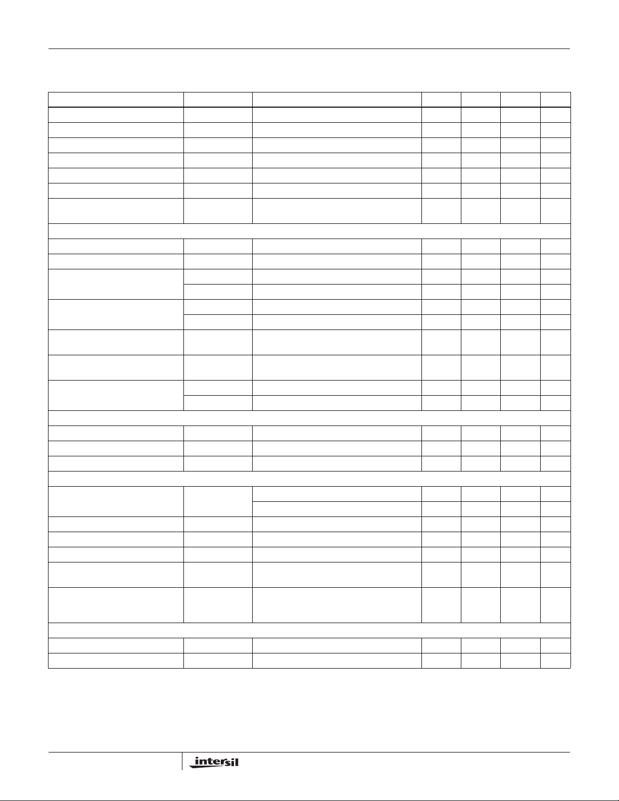
GATE DRIVER SWITCHING TIMING (refer to “ISL6262A Gate Driver Timing Diagram” on page 6)
UGATE Rise Time t
LGATE Rise Time t
UGATE Fall Time t
LGATE Fall Time t
UGATE Turn-on Propagation Delay t
LGATE Turn-on Propagation Delay t
RU
RL
FU
FL
PDHU
PDHU
PVCC= 5V, 3nF Load 8.0 ns
PVCC= 5V, 3nF Load 8.0 ns
PVCC= 5V, 3nF Load 8.0 ns
PVCC= 5V, 3nF Load 4.0 ns
PVCC= 5V, Outputs Unloaded 30 ns
PVCC= 5V, Outputs Unloaded 15 ns
BOOTSTRAP DIODE
Forward Voltage V
Leakage V
= 5V, Forward Bias Current = 2mA 0.43 0.58 0.72 V
DDP
= 16V 1 µA
R
POWER GOOD and PROTECTION MONITOR
I
PGOOD Low Voltage V
PGOOD Leakage Current I
OL
OH
= 4mA 0.26 0.4 V
PGOOD
P
= 3.3V -1 1 µA
GOOD
4
FN6343.1
December 23, 2008
ISL6262A
Electrical Specifications V
= 5V, TA = -40°C to +100°C, unless otherwise specified. Parameters with MIN and/or MAX limits are 100%
DD
tested at +25°C, unless otherwise specified. Temperature limits established by characterization and are not
production tested. (Continued)
PARAMETER SYMBOL TEST CONDITIONS MIN TYP MAX UNITS
PGOOD Delay t
Overvoltage Threshold O
Severe Overvoltage Threshold O
pgd
VH
VHS
OCSET Reference Current I (R
CLK_EN# Low to PGOOD High 6.3 7.6 8.9 ms
VO rising above setpoint >1ms 160 200 240 mV
VO rising above setpoint >0.5µs 1.675 1.7 1.725 V
) = 10µA 9.8 10 10.2 µA
BIAS
OC Threshold Offset DROOP rising above OCSET >120µs -3.5 3.5 mV
Current Imbalance Threshold Difference between ISEN1 and ISEN2 >1ms 9 mV
Undervoltage Threshold
(VDIFF-SOFT)
UV
f
VO falling below setpoint for >1ms -360 -300 -240 mV
LOGIC INPUTS
VR_ON, DPRSLPVR Input Low V
VR_ON, DPRSLPVR Input High V
Leakage Current of VR_ON I
Leakage Current of DPRSLPVR I
IL_DPRSLP(3.3V)
I
IH_DPRSLP(3.3V)
DAC(VID0-VID6), PSI# and
DPRSTP# Input Low
DAC(VID0-VID6), PSI# and
DPRSTP# Input High
Leakage Current of DAC(VID0VID6), PSI# and DPRSTP#
IL(3.3V)
IH(3.3V)
IL(3.3V)
I
IH(3.3V)
V
IL(1V)
V
IH(1V)
I
IL(1V)
I
IH(1V)
2.3 V
Logic input is low -1 0 µA
Logic input is high at 3.3V 0 1 µA
DPRSLPVR input is low -1 0 µA
DPRSLPVR input is high at 3.3V 0.45 1 µA
0.7 V
Logic input is low -1 0 µA
Logic input is high at 1V 0.45 1 µA
1V
0.3 V
THERMAL MONITOR
NTC Source Current NTC = 1.3V 53 60 67 µA
Over-Temperature Threshold V(NTC) falling 1.18 1.2 1.22 V
VR_TT# Low Output Resistance R
TT
I = 20mA 6.5 9 Ω
POWER MONITOR
PMON Output Voltage Range V
PMON Maximum Voltage V
PMON Sourcing Current I
PMON Sinking Current I
pmon
pmonmax
sc_pmon
sk_pmon
Maximum Current Sinking Capability (see Figure 31) PMON/
PMON Impedance When PMON is within its sourcing/sinking
VSEN = 1.2V, Droop - VO= 80mV 1.638 1.680 1.722 V
VSEN = 1V, Droop - V
= 20mV 0.308 0.350 0.392 V
O
2.8 3.0 V
VSEN = 1V, Droop - VO= 50mV 2 mA
VSEN = 1V, Droop - VO= 50mV 2 mA
250Ω
PMON/
180Ω
PMON/
130Ω
7 Ω
current range (Established by
characterization)
CLK_EN# OUTPUT LEVELS
CLK_EN# High Output Voltage V
CLK_EN# Low Output Voltage V
OH
OL
3V3 = 3.3V, I = -4mA 2.9 3.1 V
I
CLK_EN#
= 4mA 0.26 0.4 V
A
5
FN6343.1
December 23, 2008
ISL6262A Gate Driver Timing Diagram
PWM
t
PDHU
UGATE
t
RU
ISL6262A
t
FU
1V
LGATE
t
FL
1V
Functional Pin Description
PSI#
PMON
RBIAS
NTC
SOFT
VW
1
2
3
4
5
6
7
8
9
PGOOD
VR_TT#
OCSET
t
t
PDHL
3V3
CLK_EN#
DPRSTP#
DPRSLPVR
VR_ON
VID6
VID5
48 47 46 45 44 43 42 41 40 39 38 37
GND PAD
(BOTTOM)
RL
VID4
VID3
VID2
VID1
VID0
36
BOOT1
35
UGATE1
34
PHASE1
33
PGND1
LGATE1
32
31
PVCC
30
LGATE2
29
PGND2
PHASE2
28
COMP
FB
FB2
6
10
11
12
13 14 15 16 17 18 19 20 21 22 23 24
VDIFF
DROOP
RTN
VSEN
VO
DFB
VSUM
VIN
GND
UGATE2
27
BOOT2
26
NC
25
VDD
ISEN2
ISEN1
FN6343.1
December 23, 2008

ISL6262A
PGOOD - Power good open-drain output. Connect
externally with 680Ω to VCCP or 1.9kΩ to 3.3V.
PSI# - Current indicator input. When asserted low, indicates
a reduced load-current condition and initiates single-phase
operation.
PMON - Analog output. PMON is proportional to the product
of Vsen and droop voltage.
RBIAS - 147k resistor to GND sets internal current
reference.
VR_TT# - Thermal overload output indicator with open-drain
output. Over-temperature pull-down resistance is 10Ω.
NTC - Thermistor input to VRTT# circuit and a 60µA current
source is connected internally to this pin.
SOFT - A capacitor from this pin to GND sets the maximum
slew rate of the output voltage. SOFT is the non-inverting
input of the error amplifier.
OCSET - Overcurrent set input. A resistor from this pin to
VO sets DROOP voltage limit for OC trip. A 10µA current
source is connected internally to this pin.
VW - A resistor from this pin to COMP programs the
switching frequency (for example, 6.82kΩ ≅ 300kHz).
COMP - This pin is the output of the error amplifier.
FB - This pin is the inverting input of error amplifier.
ISEN1 - Individual current sharing sensing for Channel 1.
N/C - Not connected. Grounding this pin to signal ground in
the practical layout.
BOOT2 - This pin is the upper gate driver supply voltage for
phase 2. An internal boot strap diode is connected to the
PVCC pin.
UGATE2 - Upper MOSFET gate signal for phase 2.
PHASE2 - The phase node of phase 2. Connect this pin to
the source of the Channel 2 upper MOSFET.
PGND2 - The return path of the lower gate driver for
phase 2.
LGATE2 - Lower-side MOSFET gate signal for phase 2.
PVCC - 5V power supply for gate drivers.
LGATE1 - Lower-side MOSFET gate signal for phase 1.
PGND1 - The return path of the lower gate driver for
phase 1.
PHASE1 - The phase node of phase 1. Connect this pin to
the source of the Channel 1 upper MOSFET.
UGATE1 - Upper MOSFET gate signal for phase 1.
BOOT1 - This pin is the upper-gate-driver supply voltage for
phase 1. An internal boot strap diode is connected to the
PVCC pin.
FB2 - There is a switch between FB2 pin and the FB pin.
The switch is closed in single-phase operation and is
opened in two phase operation. The components connecting
to FB2 are to adjust the compensation in single phase
operation to achieve optimum performance.
VDIFF - This pin is the output of the differential amplifier.
VSEN - Remote core voltage sense input.
RTN - Remote core voltage sense return.
DROOP - Output of the droop amplifier. The voltage level on
this pin is the sum of V
and the droop voltage.
O
DFB - Inverting input to droop amplifier.
VO - An input to the IC that reports the local output voltage.
VSUM - This pin is connected to the summation junction of
channel current sensing.
VIN - Battery supply voltage. It is used for input voltage
feed-forward to improve input line transient performance.
GND - Signal ground. Connect to local controller ground.
VDD - 5V control power supply.
ISEN2 - Individual current sharing sensing for Channel 2. If
ISEN2 is pulled to 5V, phase 2’s gate signals are disabled.
ISL6262A is then configured in always-1-phase mode.
VID0, VID1, VID2, VID3, VID4, VID5, VID6 - VID input with
VID0 is the least significant bit (LSB) and VID6 is the most
significant bit (MSB).
VR_ON - Digital enable input. A logic high signal on this pin
enables the regulator.
DPRSLPVR - Deeper sleep enable signal. A logic high
signal on this pin indicates the micro-processor is in
deeper-sleep mode and also indicates a slow C4 entry or
exit rate with 41µA discharging or charging the SOFT
capacitor.
DPRSTP# - Deeper sleep slow wake up signal. A logic low
signal on this pin indicates the micro-processor is in
deeper-sleep mode.
CLK_EN# - Digital output for system clock. Goes active 13
clks after V
is within 10% of Boot voltage.
core
3V3 - 3.3V supply voltage for CLK_EN#.
7
FN6343.1
December 23, 2008
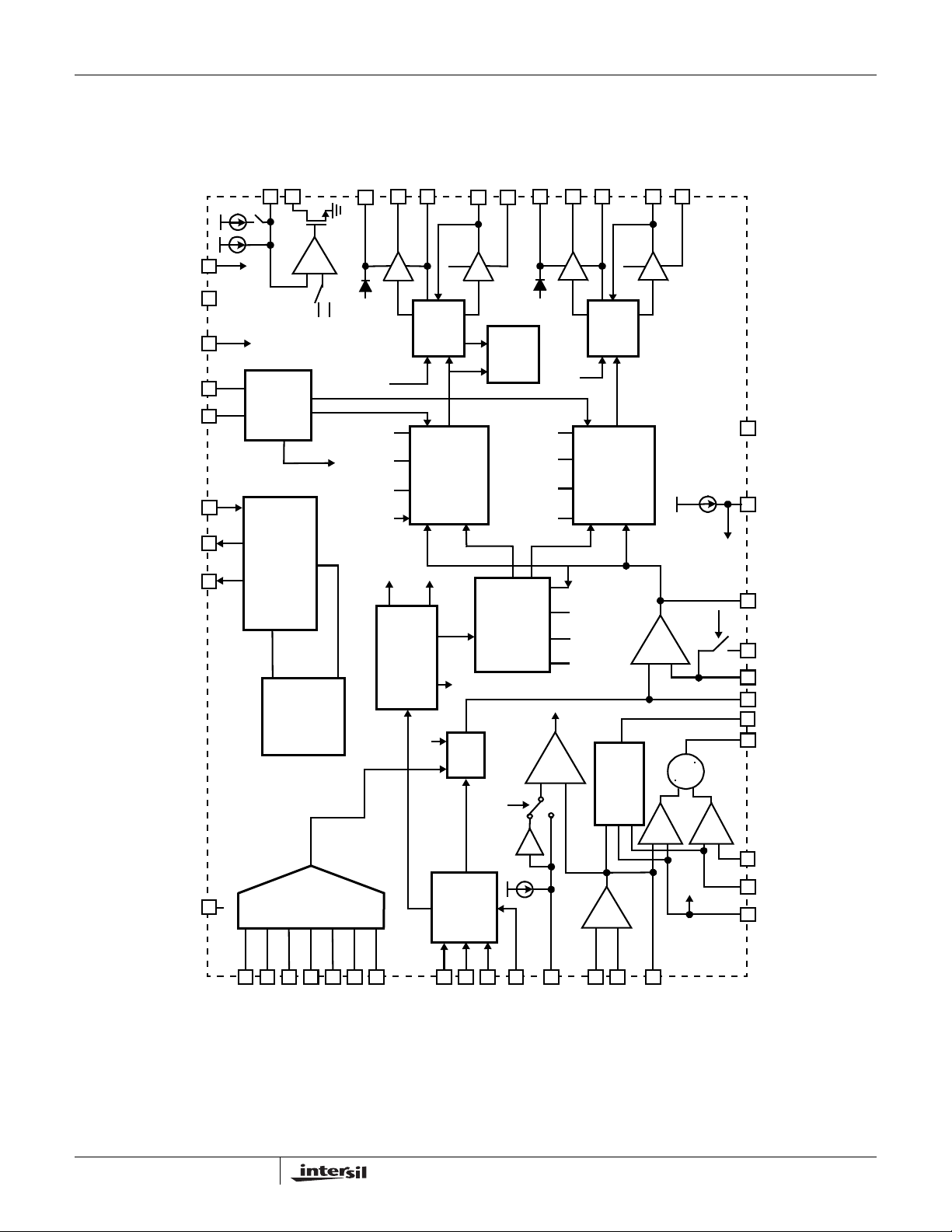
Functional Block Diagram
ISL6262A
PVCC
VDD
VIN
ISEN2
ISEN1
3V3
PGOOD
CLK_EN#
RBIAS
6µA
54µA
PVCC
VIN
NTC
VR_TT#
1.2V
CURRENT
BALANCE
PGOOD
MONITOR
AND LOGIC
P
FLT
FAULT AND
PGOOD
LOGIC
DAC
-
I_BALF
GOOD
DACOUT
+
1.24V
BOOT1
PVCC
VSOFT
VIN
OC
CH1
CH1 CH2
CONTROL
UGATE1
DRIVER
LOGIC
FLT
MODULATOR
PHASE
LOGIC
VO
REQUEST
MODE CHANGE
PHASE1
PVCC
SINGLE
PHASE
SOFT
MODE
CONTROL
LGATE1
PGND1
PVCC
ULTRA-
SONIC
TIMER
VSOFT
CH2
PHASE
SEQUENCER
SINGLE
PHASE
0.66
10µA
BOOT2
VIN
OC
-
UGATE2
DRIVER
FLT
MODULATOR
Vw
VO
VIN
OC
+
DROOP
PHASE2
PVCC
LOGIC
-
+
VSOFT
MULTIPLIER
LGATE2
E/A
+
-
1
-
+
PGND2
SINGLE
PHASE
+
VO
GND
VW
Vw
COMP
FB2
FB
SOFT
PMON
VDIFF
+
1
-
+
RTN
VSEN
VO
VID0
VID1
VID2
VID3
VID4
VID5
VID6
PSI#
VR_ON
DPRSLPVR
OCSET
DPRSTP#
DFB
VSUM
FIGURE 1. SIMPLIFIED FUNCTIONAL BLOCK DIAGRAM OF ISL6262A
8
DROOP
FN6343.1
December 23, 2008
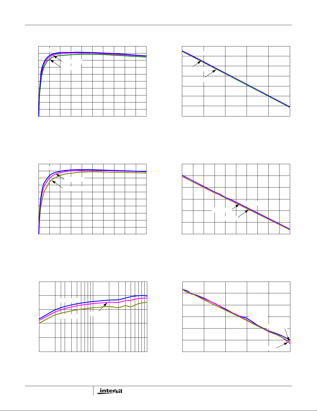
V
(V)
ISL6262A
Typical Performance Curves 300kHz Operation, 2xIRF7821 as Upper Devices and 2xIRF7832 as Bottom Devices
100
VIN = 8.0V
90
80
70
60
50
40
EFFICIENCY (%)
30
20
10
0
0 5 10 15 20 25 30 35 40 45 50
VIN = 12.6V
V
= 19.0V
IN
I
OUT
(A)
FIGURE 2. ACTIVE MODE EFFICIENCY , 2 PHASE, CCM,
PSI# = HIGH, VID = 1.15V
100
VIN = 8.0V
90
80
70
60
50
40
EFFICIENCY (%)
30
20
10
0
02468101214161820
VIN = 12.6V
VIN = 19.0V
I
OUT
(A)
FIGURE 4. ACTIVE MODE EFFICIENCY , 1 PHASE, CCM,
PSI# = LOW, VID = 1.15V
1.16
VIN = 8.0V
VIN = 12.6V
= 19.0V
V
IN
01020304050
I
(A)
OUT
(V)
OUT
V
1.14
1.12
1.10
1.08
1.06
1.04
1.02
FIGURE 3. ACTIVE MODE LOAD LINE, 2 PHASE, CCM,
PSI# = HIGH, VID = 1.15V
1.16
1.15
1.14
(V)
1.13
OUT
V
1.12
1.11
1.10
0 4 6 8 10 20
2 12141618
VIN = 12.6V
VIN = 19.0V
I
OUT
VIN = 8.0V
(A)
FIGURE 5. ACTIVE MODE LOAD LINE, 1 PHASE, CCM,
PSI# = LOW, VID = 1.15V
100
90
80
70
EFFICIENCY (%)
60
50
0.1 1.0 10
FIGURE 6. DEEPER SLEEP MODE EFFICIENCY FIGURE 7. DEEPER SLEEP MODE LOAD LINE
VIN = 8.0V
VIN = 19.0V
VIN = 12.6V
I
(A)
OUT
9
0.765
0.760
0.755
0.750
OUT
0.745
0.740
0.735
0246810
I
OUT
(A)
VIN = 8.0V
VIN = 12.6V
VIN = 19.0V
FN6343.1
December 23, 2008
 Loading...