®
ISL6256, ISL6256A
Data Sheet July 19, 2007
Highly Integrated Battery Charger with
Automatic Power Source Selector for
Notebook Computers
The ISL6256, ISL6256A is a highly integrated battery charger
controller for Li-Ion/Li-Ion polymer batteries. High Effici ency is
achieved by a synchronous buck topology and the use of a
MOSFET, instead of a diode, for selecting power from the
adapter or battery . The low side MOSFET emulates a diode at
light loads to improve the light load efficiency and prevent
system bus boosting.
The constant output voltage can be selected for 2, 3 and 4
series Li-Ion cells with 0.5% accuracy over-temperature. It
can also be programmed between 4.2V+5%/cell and 4.2V5%/cell to optimize battery capacity. When supplying the load
and battery charger simultaneously, the input current limit for
the AC adapter is programmable to within 3% accuracy to
avoid overloading the AC adapter, and to allow the system to
make efficient use of available adapter po wer for charging . It
also has a wide range of programmable charging current. The
ISL6256, ISL6256A provides outputs that are used to monitor
the current drawn from the AC adapter , and monito r for th e
presence of an AC adapter. The ISL6256, ISL6256A
automatically transitions from regulating current mode to
regulating voltage mode.
ISL6256, ISL6256A has a feature for automatic power source
selection by switching to the battery when the AC adapter is
removed or switching to the AC adapter when the AC adapter
is available. It also provides a DC adapter monitor to support
aircraft power applications with the option of no battery
charging.
Ordering Information
PART
NUMBER
(Notes 1, 2)
ISL6256HRZ* ISL 6256HRZ -10 to +100 28 Ld 5x5 QFN L28.5×5
ISL6256HAZ* ISL 6256HAZ -10 to +100 28 Ld QSOP M28.15
ISL6256AHRZ* ISL6256 AHRZ -10 to +100 28 Ld 5x5 QFN L28.5×5
ISL6256AHAZ* ISL6256 AHAZ -10 to +100 28 Ld QSOP M28.15
NOTES:
1. Intersil Pb-free plus anneal products employ special Pb-free material
sets; molding compounds/die attach materials and 100% matte tin
plate termination finish, which are RoHS compliant and compatible
with both SnPb and Pb-free soldering operations. Intersil Pb-free
products are MSL classified at Pb-free peak reflow temperatures tha t
meet or exceed the Pb-free requirements of IPC/JEDEC J STD-0 20.
2. *Add “-T” for Tape and Re el. Please refer to TB347 for details on reel
specifications.
PART
MARKING
TEMP
RANGE
(°C)
PACKAGE
(Pb-free)
PKG.
DWG. #
FN6499.1
Features
• ±0.5% Charge Voltage Accuracy (-10°C to +100°C)
• ±3% Accurate Input Current Limit
• ±3% Accurate Battery Charge Current Limit
• ±25% Accurate Battery Trickle Charge Current Limit
• Programmable Charge Current Limit, Adapter Current
Limit and Charge Voltage
• Fixed 300kHz PWM Synchronous Buck Controller with
Diode Emulation at Light Load
• Overvoltage Protection
• Output for Current Drawn from AC Adapter
• AC Adapter Present Indicator
• Fast Input Current Limit Response
• Input Voltage Range 7V to 25V
• Support 2-, 3- and 4-Cells Battery Pack
• Up to 17.64V Battery-Voltage Set Point
• Control Adapter Power Source Select MOSFET
• Thermal Shutdown
• Aircraft Power Capable
• DC Adapter Present Indicator
• Battery Discharge MOSFET Control
• Less than 10µA Battery Leakage Current
• Supports Pulse Charging
• Pb-Free Plus Anneal Available (RoHS Compliant)
Applications
• Notebook, Desknote and Sub-notebook Computers
• Personal Digital Assistant
1
CAUTION: These devices are sensitive to electrostatic discharge; follow proper IC Handling Procedures.
1-888-INTERSIL or 1-888-468-3774
| Intersil (and design) is a registered trademark of Intersil Americas Inc.
All other trademarks mentioned are the property of their respective owners.
Copyright Intersil Americas Inc. 2007. All Rights Reserved
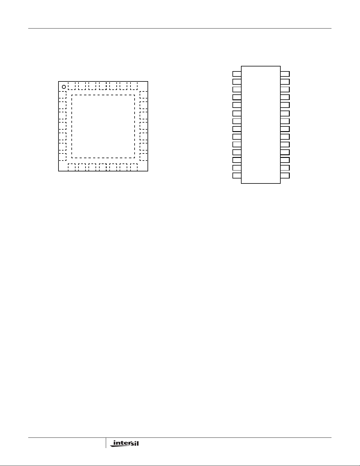
Pinouts
ISL6256, ISL6256A
(28 LD QFN)
TOP VIEW
ISL6256, ISL6256A
ISL6256, ISL6256A
(28 LD QSOP)
TOP VIEW
EN
CELLS
ICOMP
VCOMP
ICM
VREF
CHLIM
DCSET
ACSET
VDD
DCIN
28 27 26 25 24 23 22
1
2
3
4
5
6
7
8 9 10 11 12 13 14
GND
ACLIM
VADJ
PGND
PGND
PGND
DCPRN
LGATE
ACPRN
VDDP
CSON
21
20
19
18
17
16
15
BOOT
CSOP
CSIN
CSIP
SGATE
BGATE
PHASE
UGATE
DCIN
VDD
ACSET
DCSET
EN
CELLS
ICOMP
VCOMP
ICM
VREF
CHLIM
ACLIM
VADJ
GND
1 28
2 27
3 26
4 25
5 24
6 23
7 22
8 21
9 20
10 19
11 18
12 17
13 16
14 15
DCPRN
ACPRN
CSON
CSOP
CSIN
CSIP
SGATE
BGATE
PHASE
UGATE
BOOT
VDDP
LGATE
PGND
2
FN6499.1
July 19, 2007
ISL6256, ISL6256A
ACSET
ACPRN
ACLIM
ICOMP
VCOMP
VADJ
CELLS
VREF
VREF
152kΩ
152kΩ
VREF
514kΩ
514kΩ
VOLTAGE
SELECTOR
REFERENCE
VDD
+
-
ADAPTER
CURRENT
LIMIT SET
gm1
+
2.1V
ICM CSIP CSIN
1.26V
SGATE
-
gm3
+
MIN
CURRENT
BUFFER
MIN
VOLTAGE
BUFFER
-
288kΩ
32kΩ
16kΩ
48kΩ
Σ
-0.25
CA2
X19.9
-
-
+
gm2
X19.9
CA1
+
+
-
CSON
300kHz
RAMP
1.26V
-
PWM
+
+
-
-
+
LDO
REGULATOR
-
+
DCSET
DCPRN
BGATE
DCIN
VDD
BOOT
UGATE
PHASE
VDDP
LGATE
PGND
1.065V
EN
GND
FB
CSON
CSOP
CHLIM
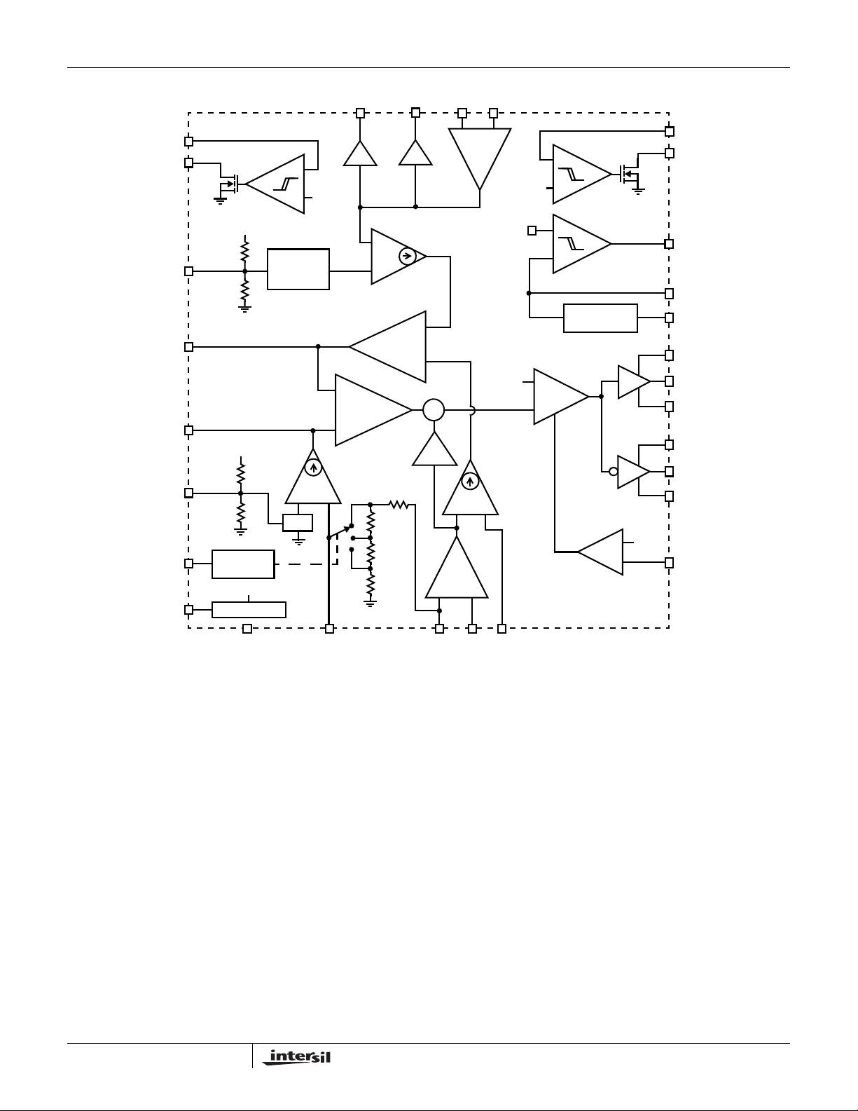
FIGURE 1. FUNCTIONAL BLOCK DIAGRAM
3
FN6499.1
July 19, 2007
AC ADAPTER
ISL6256, ISL6256A
Q3
Q3
Q3
Q3
TO HOST
CONTROLLER
VREF
VREF
4.7k
CHARGE
CHARGE
CHARGE
CHARGE
ENABLE
ENABLE
ENABLE
ENABLE
R12
R12
2.6A CHARGE LIMIT
2.6A CHARGE LIMIT
20k 1%
20k 1%
253mA TRICKLE CHARGE
1.87k
1.87k
1.87k
1.87k
TRICKLE
TRICKLE
TRICKLE
TRICKLE
CHARGE
CHARGE
CHARGE
CHARGE
R8
R8
R8
R8
130k
130k
130k
130k
1%
1%
1%
1%
R9
10.2k
1%
1%
1%
3.3V
3.3V
C6
R6
FLOATING
FLOATING
4.2V/CELL
4.2V/CELL
R13
R13
1%
1%
1%
1%
C7
C7
1µF
1
1
1
R5
R5
R5
R5
100k
100k
6.8nF
C5
Q6
10nF
R11
R11
130k
130k
130k
130k
1%
1%
1%
1%
VDD
R10
R10
R10
R10
4.7
4.7Ω
1
1µF
1
1
C9
C9
Q5
Q5
C8
C8
0.1µF
DCIN
DCIN
DCIN
DCIN
ACSET
ACSET
ACSET
ACSET
IS
VDDP
VDDP
VDDP
VDDP
VDD
VDD
VDD
VDD
ACPRN
ACPRN
ACPRN
ACPRN
ICOMP
ICOMP
ICOMP
ICOMP
VCOMP
VCOMP
VCOMP
VCOMP
VADJ
VADJ
VADJ
VADJ
EN
EN
EN
EN
ACLIM
ACLIM
ACLIM
ACLIM
VREF
VREF
VREF
VREF
CHLIM
CHLIM
CHLIM
CHLIM
CSON
ISL6256
ISL6256
ISL6256
ISL
ISL6256A
ISL
ISL
SGATE
SGATE
SGATE
SGATE
CSIP
CSIP
CSIP
CSIP
CSIN
CSIN
CSIN
CSIN
BGATE
BGATE
BGATE
BGATE
BOOT
BOOT
BOOT
BOOT
UGATE
UGATE
UGATE
UGATE
PHASE
PHASE
PHASE
PHASE
LGATE
LGATE
LGATE
LGATE
PGND
PGND
PGND
PGND
CSOP
CSOP
CSOP
CSOP
CSON
CSON
CSON
CSON
CELLS
CELLS
CELLS
CELLS
ICM
ICM
ICM
ICM
GND
GND
GND
GND
R21
C2
C2
0.1
0.1
0.1
0.1µF
R22
R7: 100Ω
2.2Ω
22Ω
VDDP
VDDP
VDDP
VDDP
D2
D2
D2
D2
C4
C4
0.1
0.1µF
0.1
0.1
Q2
Q2
R11
C3C3
0.047uF
R12
VDD
VDD
VDD
VDD
4 CELLS
4 CELLS
R2
R2
R2
R2
20m
20m
20m
20mΩ
C1:10
C1:10µF
Q1
Q1
22Ω
22Ω
C11
C11
3300pF
3300pF
D1
OPTIONAL
Q4
Q4
L
4.7µH
R1
R1
R1
R1
20mΩ
C10
22uF
SYSTEM LOAD
SYSTEM LOAD
BAT+
BAT+
BAT+
BAT+
BATTERY
PACK
BAT-
BAT-
BAT-
BAT-
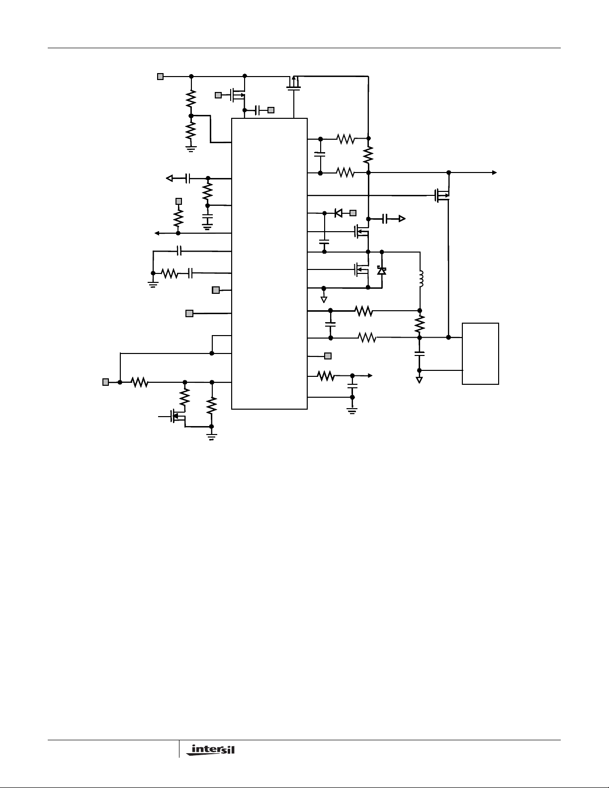
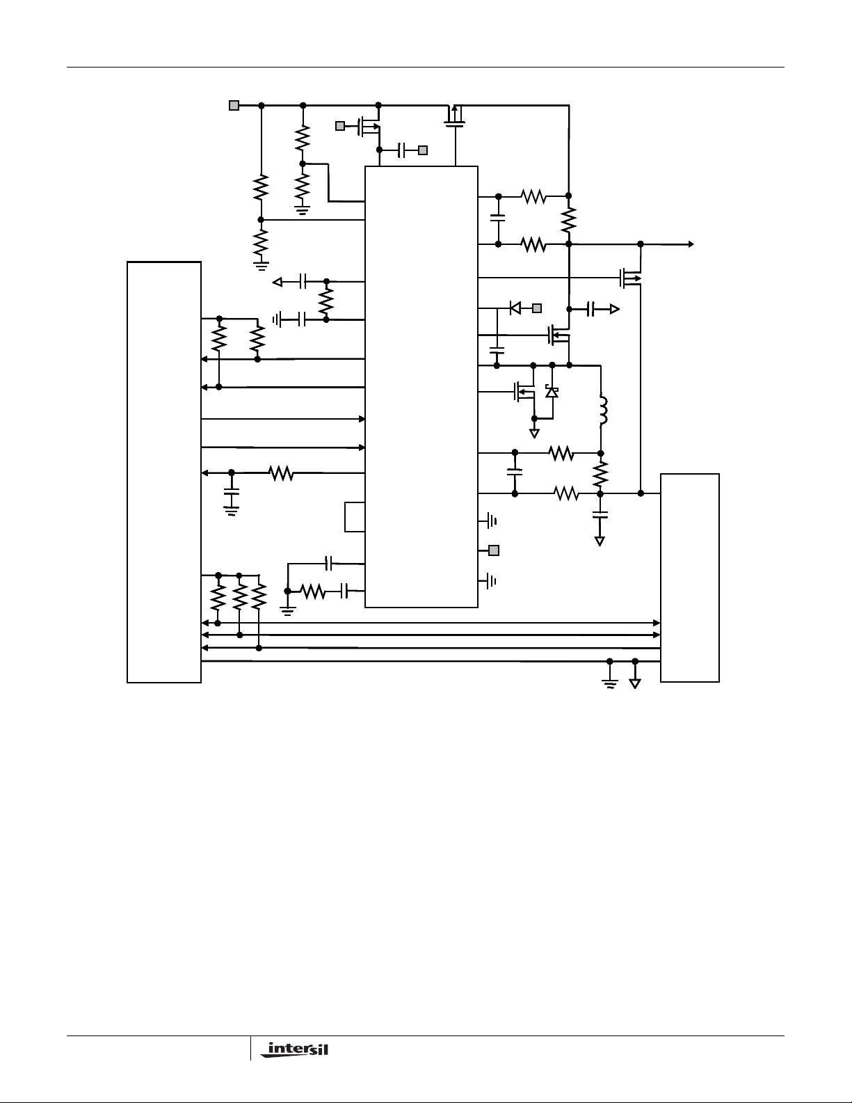
FIGURE 2. ISL6256, ISL6256A TYPICAL APPLICATION CIRCUIT WITH FIXED CHARGING PARAMETERS
4
FN6499.1
July 19, 2007
VCC
VCC
VCC
DIGITAL
DIGITAL
DIGITAL
INPUT
DIGITAL
DIGITAL
DIGITAL
INPUT
INPUT
INPUT
D/A OUTPUT
D/A OUTPUT
D/A OUTPUT
OUTPUT
OUTPUT
OUTPUT
A/D INPUT
A/D INPUT
A/D INPUT
HOST
HOST
HOST
HOST
AVDD/VREF
AVDD/VREF
AVDD/VREF
SCL
SCL
SCL
SDL
SDL
SDL
A/D INPUT
A/D INPUT
A/D INPUT
GND
GND
GND
GND
ADAPTER
R14
R14
100k
100k
100k
100k
1%
1%
1%
1%
R15
R15
11.5k
11.5k
1%
1%
R16
100k
100k
100k
100k
C11
C11
3300pF
3300pF
R11, R12
R13: 10k
VDD
VDD
VDD
VDD
R8
R8
R8
R8
130k
130k
130k
130k
1%
1%
1%
1%
R9
R9
R9
R9
10.2k
10.2k
10.2k
10.2k
1%
1%
1%
1%
C7
C7
µF
1
1
C9
C9
1µF
1
R5
R5
R5
R5
100k
100k
100k
100k
R7: 100Ω
R7:
5.15A INPUT
5.15A INPUT
5.15A INPUT
CURRENT LIMIT
CURRENT LIMIT
CURRENT LIMIT
CURRENT LIMIT
C6
C6
6.8nF
6.8nF
6.8nF
6.8nF
R6
R6
R6
R6
4.7k
ISL6256, ISL6256A
C8
C8
0.1µF
0.1
0.1
0.1
ISL
ISL
ISL
ISL
CSON
ISL6256
ISL6256A
SGATE
SGATE
SGATE
CSIP
CSIP
CSIN
CSIN
BGATE
BGATE
BGATE
BOOT
BOOT
BOOT
UGATE
UGATE
UGATE
PHASE
PHASE
PHASE
LGATE
LGATE
LGATE
PGND
PGND
PGND
CSOP
CSOP
CSOP
CSON
CSON
CSON
CELLS
CELLS
CELLS
VADJ
VADJ
GND
GND
R10
R10
4.7
4.7
4.7
4.7Ω
VREF
VREF
VREF
VREF
C5
C5
10nF
10nF
10nF
10nF
Q5
Q5
DCIN
DCIN
DCIN
ACSET
ACSET
ACSET
DCSET
DCSET
DCSET
VDDP
VDDP
VDDP
VDD
VDD
VDD
ACPRN
ACPRN
ACPRN
DCPRN
DCPRN
DCPRN
CHLIM
CHLIM
CHLIM
EN
EN
EN
ICM
ICM
ICM
ACLIM
ACLIM
ACLIM
VREF
VREF
VREF
ICOMP
ICOMP
ICOMP
VCOMP
VCOMP
VCOMP
CSIP
CSIN
VADJ
GND
Q3
Q3
Q3
Q3
R21
C2
C2
0.1
0.1
0.1
0.1µF
R22
VDDP
VDDP
D2
D2
C4
C4
0.1µF
0.1
0.1
0.1
Q2
Q2
GND
GND
GND
GND
3 CELLS
3 CELLS
3 CELLS
3 CELLS
FLOATING
FLOATING
4.2V/CELL
4.2V/CELL
4.2V/CELL
4.2V/CELL
2.2Ω
22Ω
R11
C3C3
0.047uF
R12
R2
R2
R2
R2
20m
20m
20m
20mΩ
C1:10µF
C1:10
C1:10
C1:10
Q1
Q1
Q1
Q1
D1
D1
OPTIONAL
22Ω
22Ω
L
4.7µH
R1
R1
R1
R1
20mΩ
C10
22µF
SYSTEM LOAD
SYSTEM LOAD
Q4
Q4
Q4
Q4
BAT+
BATTERY
BATTERY
PACK
SCL
SCL
SCL
SCL
SDL
SDL
SDL
SDL
TEMP
TEMP
TEMP
BAT-
BAT-
BAT-
BAT-
FIGURE 3. ISL6256, ISL6256A TYPICAL APPLICATION CIRCUIT WITH µP CONTROL AND AIRCRAFT POWER SUPPORT
5
FN6499.1
July 19, 2007
ISL6256, ISL6256A
Absolute Maximum Ratings Thermal Information
DCIN, CSIP, CSON to GND. . . . . . . . . . . . . . . . . . . . .-0.3V to +28V
CSIP-CSIN, CSOP-CSON. . . . . . . . . . . . . . . . . . . . . -0.3V to +0.3V
CSIP-SGATE, CSIP-BGATE . . . . . . . . . . . . . . . . . . . . .-0.3V to 16V
PHASE to GND . . . . . . . . . . . . . . . . . . . . . . . . . . . . . . . . -7V to 30V
BOOT to GND . . . . . . . . . . . . . . . . . . . . . . . . . . . . . . .-0.3V to +35V
BOOT to VDDP . . . . . . . . . . . . . . . . . . . . . . . . . . . . . . . . -2V to 28V
ACLIM, ACPRN, CHLIM, DCPRN, VDD to GND. . . . . . .-0.3V to 7V
BOOT-PHASE, VDDP-PGND . . . . . . . . . . . . . . . . . . . . . -0.3V to 7V
ACSET and DCSET to GND (Note 3) . . . . . . . -0.3V to VDD +0.3V
ICM, ICOMP, VCOMP to GND. . . . . . . . . . . . . .-0.3V to VDD +0.3V
VREF, CELLS to GND . . . . . . . . . . . . . . . . . . . . -0.3V to VDD +0.3V
EN, VADJ, PGND to GND . . . . . . . . . . . . . . . . . -0.3V to VDD +0.3V
UGATE. . . . . . . . . . . . . . . . . . . . . . . . PHASE -0.3V to BOOT +0.3V
LGATE. . . . . . . . . . . . . . . . . . . . . . . . . PGND -0.3V to VDDP +0.3V
CAUTION: Do not operate at or near the maximum ratings listed for extended periods of time. Exposure to such conditions may adversely impact product reliability and
result in failures not covered by warranty.
NOTES:
3. ACSET may be operated 1V below GND if the current through ACSET is limited to less than 1mA.
is measured in free air with the component mounted on a high effective thermal conductivity test board with “direct attach” features. See T ech
4. θ
JA
Brief TB379.
5. For θ
, the “case temp” location is the center of the exposed metal pad on the package underside.
JC
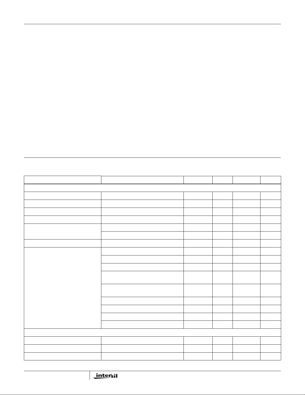
Electrical Specifications DCIN= CSIP = CSIN = 18V, CSOP = CSON = 12V, ACSET = DCSET = 1.5V, ACLIM = VREF,
VADJ=Floating, EN=VDD=5V, BOOT-PHASE=5.0V, GND=PGND=0V, C
T
= -10°C to +100°C, TJ≤+125°C, Unless Otherwise Noted.
A
PARAMETER TEST CONDITIONS MIN TYP MAX UNITS
SUPPLY AND BIAS REGULATOR
DCIN Input Voltage Range 7 25 V
DCIN Quiescent Current EN = VDD or GND, 7V ≤ DCIN ≤ 25V 1.4 3 mA
Battery Leakage Current (Note 6) DCIN = 0, no load 3 10 µA
VDD Output Voltage/Regulation 7V ≤ DCIN ≤ 25V, 0 ≤ I
VDD Undervoltage Lockout Trip Point VDD Rising 4.0 4.4 4.6 V
Hysteresis 200 250 400 mV
Reference Output Voltage VREF 0 ≤ I
≤ 300µA 2.365 2.39 2.415 V
VREF
Battery Charge Voltage Accuracy CSON = 16.8V, CELLS = VDD, VADJ = Float -0.5 0.5 %
CSON = 12.6V, CELLS = GND, VADJ = Float -0.5 0.5 %
CSON = 8.4V, CELLS = Float, VADJ = Float -0.5 0.5 %
CSON = 17.64V, CELLS= VDD,
VADJ= VREF
CSON = 13.23V, CELLS = GND,
VADJ= VREF
CSON = 8.82V, CELLS= Float, VADJ = VREF -0.5 0.5 %
CSON = 15.96V, CELLS= VDD, VADJ = GND -0.5 0.5 %
CSON = 11.97V , CELLS= GND, VADJ = GND -0.5 0.5 %
CSON = 7.98V, CELLS = Float, VADJ = GND -0.5 0.5 %
TRIP POINTS
ACSET Threshold 1.24 1.26 1.28 V
ACSET Input Bias Current Hysteresis 2.4 3.4 4.4 µA
ACSET Input Bias Current ACSET ≥ 1.26V 2.4 3.4 4.4 µA
VDD
Thermal Resistance θ
(°C/W) θJC (°C/W)
JA
QFN Package (Notes 4, 5). . . . . . . . . . 39 9.5
QSOP Package (Note 4) . . . . . . . . . . . 80 NA
Junction Temperature Range. . . . . . . . . . . . . . . . . .-10°C to +150°C
Operating Temperature Range . . . . . . . . . . . . . . . .-10°C to +100°C
Storage Temperature. . . . . . . . . . . . . . . . . . . . . . . .-65°C to +150°C
Pb-free reflow profile . . . . . . . . . . . . . . . . . . . . . . . . . .see link below
http://www.intersil.com/pbfree/Pb-FreeReflow.asp
VDD
=1µF, I
VDD
=0mA,
≤ 30mA 4.925 5.075 5.225 V
-0.5 0.5 %
-0.5 0.5 %
6
FN6499.1
July 19, 2007
ISL6256, ISL6256A
Electrical Specifications DCIN= CSIP = CSIN = 18V, CSOP = CSON = 12V, ACSET = DCSET = 1.5V, ACLIM = VREF,
VADJ=Floating, EN=VDD=5V, BOOT-PHASE=5.0V, GND=PGND=0V, C
T
= -10°C to +100°C, TJ≤+125°C, Unless Otherwise Noted. (Continued)
A
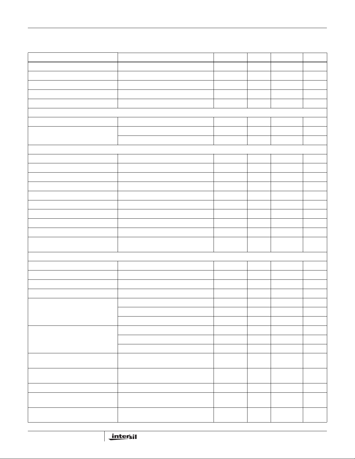
PARAMETER TEST CONDITIONS MIN TYP MAX UNITS
ACSET Input Bias Current ACSET < 1.26V -1 0 1 µA
DCSET Threshold 1.24 1.26 1.28 V
DCSET Input Bias Current Hysteresis 2.4 3.4 4.4 µA
DCSET Input Bias Current DCSET ≥ 1.26V 2.4 3.4 4.4 µA
DCSET Input Bias Current DCSET < 1.26V -1 0 1 µA
OSCILLATOR
Frequency 245 300 355 kHz
PWM Ramp Voltage (peak-peak) CSIP = 18V 1.6 V
CSIP = 11V 1 V
SYNCHRONOUS BUCK REGULATOR
Maximum Duty Cycle 97 99 99.6 %
UGATE Pull-Up Resistance BOOT-PHASE= 5V, 500mA source current 1.8 3.0 Ω
UGATE Source Current BOOT-PHASE = 5V, BOOT-UGATE = 2.5V 1.0 A
UGATE Pull-down Resistance BOOT-PHASE = 5V, 500mA sink current 1.0 1.8 Ω
UGATE Sink Current BOOT-PHASE = 5V, UGATE-PHASE = 2.5V 1.8 A
LGATE Pull-Up Resistance VDDP-PGND = 5V, 500mA source current 1.8 3.0 Ω
LGATE Source Current VDDP-PGND = 5V, VDDP-LGATE = 2.5V 1.0 A
LGATE Pull-Down Resistance VDDP-PGND = 5V, 500mA sink current 1.0 1.8 Ω
LGATE Sink Current VDDP-PGND = 5V, LGATE = 2.5V 1.8 A
Dead Time Falling UGATE to rising LGATE or
falling LGATE to rising UGATE
CHARGING CURRENT SENSING AMPLIFIER
Input Common-Mode Range 0 18 V
Input Bias Current at CSOP 5 < CSOP < 18V 0.25 2 µA
Input Bias Current at CSON 5 < CSON < 18V 75 100 µA
CHLIM Input Voltage Range 0 3.6 V
ISL6256
CSOP to CSON Full-Scale Current Sense
Voltage
ISL6256A
CSOP to CSON Full-Scale Current Sense
Voltage
ISL6256 CSOP to CSON Full-Scale
Current Sense Voltage formula
ISL6256A CSOP to CSON Full-Scale
Current Sense Voltage formula
CHLIM Input Bias Current CHLIM = GND or 3.3V, DCIN = 0V -1 1 µA
CHLIM Power-Down Mode Threshold
Voltage
CHLIM Power-Down Mode Hysteresis
Voltage
ISL6256: CHLIM = 3.3V 160 165 170 mV
ISL6256: CHLIM = 2.0V 95 100 105 mV
ISL6256: CHLIM = 0.2V 5.0 10 15.0 mV
ISL6256A: CHLIM = 3.3V 161.7 165 168.3 mV
ISL6256A: CHLIM = 2.0V 97 100 103 mV
ISL6256A: CHLIM = 0.2V 7.5 10 12.5 mV
Charge current limit mode
0.2V < CHLIM < 3.3V
Charge current limit mode
0.2V < CHLIM < 3.3V
CHLIM rising 80 88 95 mV
10 30 ns
CHLIM*50
-5
CHLIM*49.72
-2.4
15 25 40 mV
=1µF, I
VDD
CHLIM*50
CHLIM*50.28
+5
+2.4
VDD
=0mA,
mV
mV
7
FN6499.1
July 19, 2007
ISL6256, ISL6256A
Electrical Specifications DCIN= CSIP = CSIN = 18V, CSOP = CSON = 12V, ACSET = DCSET = 1.5V, ACLIM = VREF,
VADJ=Floating, EN=VDD=5V, BOOT-PHASE=5.0V, GND=PGND=0V, C
T
= -10°C to +100°C, TJ≤+125°C, Unless Otherwise Noted. (Continued)
A
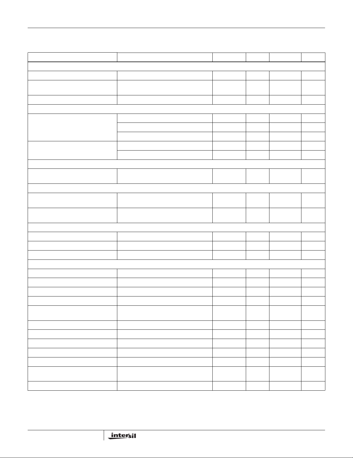
PARAMETER TEST CONDITIONS MIN TYP MAX UNITS
ADAPTER CURRENT SENSING AMPLIFIER
Input Common-Mode Range 7 25 V
Input Bias Current at CSIP and CSIN
Combined
Input Bias Current at CSIN 0 < CSIN < DCIN 0.10 µA
ADAPTER CURRENT LIMIT THRESHOLD
CSIP to CSIN Full-Scale Current Sense
Voltage
ACLIM Input Bias Current ACLIM = VREF 10 16 20 µA
VOLTAGE REGULATION ERROR AMPLIFIER
Error Amplifier Transconductance from
CSON to VCOMP
CURRENT REGULATION ERROR AMPLIFIER
Charging Current Error Amplifier
Transconductance
Adapter Current Error Amplifier
Transconductance
BATTERY CELL SELECTOR
CELLS Input Voltage for 4 Cell Select 4.3 V
CELLS Input Voltage for 3 Cell Select 2V
CELLS Input Voltage for 2 Cell Select 2.1 4.2 V
MOSFET DRIVER
BGATE Pull-Up Current CSIP-BGATE = 3V 10 30 45 mA
BGATE Pull-Down Current CSIP-BGATE = 5V 2.7 4.0 5.0 mA
CSIP-BGATE Voltage High 8 9.6 11 V
CSIP-BGATE Voltage Low -50 0 50 mV
DCIN-CSON Threshold for CSIP-BGATE
Going High
DCIN-CSON Threshold Hysteresis 250 300 400 mV
SGATE Pull-Up Current CSIP-SGATE = 3V 7 12 15 mA
SGATE Pull-Down Current CSIP-SGATE = 5V 50 160 370 µA
CSIP-SGATE Voltage High 8 9 11 V
CSIP-SGATE Voltage Low -50 0 50 mV
CSIP-CSIN Threshold for CSIP-SGATE
Going High
CSIP-CSIN Threshold Hysteresis 2 5 8 mV
CSIP = CSIN = 25V 100 130 µA
ACLIM = VREF 97 100 103 mV
ACLIM = Float 72 75 78 mV
ACLIM = GND 47 50 53 mV
ACLIM = GND -20 -16 -10 µA
CELLS = VD D 30 µA/V
DCIN = 12V, CSON Rising -100 0 100 mV
2.5 8 13 mV
=1µF, I
VDD
50 µA/V
50 µA/V
VDD
=0mA,
8
FN6499.1
July 19, 2007
ISL6256, ISL6256A
Electrical Specifications DCIN= CSIP = CSIN = 18V, CSOP = CSON = 12V, ACSET = DCSET = 1.5V, ACLIM = VREF,
VADJ=Floating, EN=VDD=5V, BOOT-PHASE=5.0V, GND=PGND=0V, C
T
= -10°C to +100°C, TJ≤+125°C, Unless Otherwise Noted. (Continued)
A
PARAMETER TEST CONDITIONS MIN TYP MAX UNITS
LOGIC INTERFACE
EN Input Voltage Range 0VDDV
EN Threshold Voltage Rising 1.030 1.06 1.100 V
Falling 0.985 1.000 1.025 V
Hysteresis 30 60 90 mV
EN Input Bias Current EN = 2.5V 1.8 2.0 2.2 µA
ACPRN Sink Current ACPRN = 0.4V 3 8 11 mA
ACPRN Leakage Current ACPRN = 5V -0.5 0.5 µA
DCPRN Sink Current DCPRN = 0.4V 3 8 11 mA
DCPRN Leakage Current DCPRN = 5V -0.5 0.5 µA
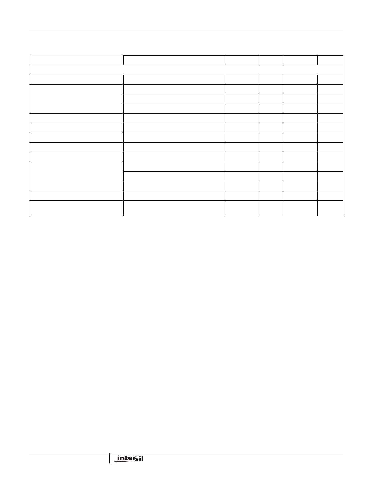
ICM Output Accuracy
= 19.9 x (V
(V
ICM
CSIP-VCSIN
))
CSIP-CSIN = 100mV -3 0 +3 %
CSIP-CSIN = 75mV -4 0 +4 %
CSIP-CSIN = 50mV -5 0 +5 %
Thermal Shutdown Temperature 150 °C
Thermal Shutdown Temperature
Hysteresis
NOTE:
6. This is the sum of currents in these pins (CSIP, CSIN, BGATE, BOOT, UGATE, PHASE, CSOP, CSON) all tied to 16.8V . No current in pins EN,
ACSET, DCSET, VADJ, CELLS, ACLIM, CHLIM.
VDD
=1µF, I
VDD
=0mA,
25 °C
9
FN6499.1
July 19, 2007
 Loading...