

®
ISL6252, ISL6252A
Data Sheet July 19, 2007
Highly Integrated Battery Charger
Controller for Notebook Computers
The ISL6252, ISL6252A is a highly integrated battery charger
controller for Li-Ion/Li-Ion polymer batteries. High Effici ency is
achieved by a synchronous buck topology. The low side
MOSFET emulates a diode at light loads to improve the light
load efficiency and prevent system bus boosting.
The constant output voltage can be selected for 2, 3 and 4
series Li-Ion cells with 0.5% accuracy over-temperature. It
can also be programmed between 4.2V + 5%/cell and
4.2V - 5%/cell to optimize battery capacity. When supplying
the load and battery charger simultaneously, the input current
limit for the AC adapter is programmable to within 3%
accuracy to avoid overloading the AC adapter , and to all ow
the system to make efficient use of available adapter power
for charging. It also has a wide range of programmable
charging current. The ISL6252, ISL6252A provides outputs
that are used to monitor the current drawn from the AC
adapter, and monito r for the presence of an AC adapter. The
ISL6252, ISL6252A automatically transitions from regulatin g
current mode to regulating voltage mode.
Ordering Information
PART
NUMBER
(Notes 1, 2)
ISL6252HRZ* ISL 6252HRZ -10 to +100 28 Ld 5x5 QFN L28.5×5
ISL6252HAZ* ISL 6252HAZ -10 to +100 24 Ld QSOP M24.15
ISL6252AHRZ* ISL6252 AHRZ -10 to +100 28 Ld 5x5 QFN L28.5×5
ISL6252AHAZ* ISL6252 AHAZ -10 to +100 24 Ld QSOP M24.15
NOTES:
1. Intersil Pb-free plus anneal products employ special Pb-free material
sets; molding compounds/die attach materials and 100% matte tin
plate termination finish, which are RoHS compliant and compatible
with both SnPb and Pb-free soldering operations. Intersil Pb-free
products are MSL classified at Pb-free peak reflow temperatures that
meet or exceed the Pb-free requirements of IPC/JEDEC J STD-0 20.
2. Add “-T” for Tape and Reel. Please refer to TB347 for details on reel
specifications.
PART
MARKING
TEMP
RANGE
(°C)
PACKAGE
(Pb-free)
PKG.
DWG. #
FN6498.1
Features
• ±0.5% Charge Voltage Accuracy (-10°C to +100°C)
• ±3% Accurate Input Current Limit
• ±3% Accurate Battery Charge Current Limit
• ±25% Accurate Battery Trickle Charge Current Limit
• Programmable Charge Current Limit, Adapter Current
Limit and Charge Voltage
• Fixed 300kHz PWM Synchronous Buck Controller with
Diode Emulation at Light Load
• Overvoltage Protection
• Output for Current Drawn from AC Adapter
• AC Adapter Present Indicator
• Fast Input Current Limit Response
• Input Voltage Range 7V to 25V
• Support 2-, 3- and 4-Cells Battery Pack
• Up to 17.64V Battery-Voltage Set Point
• Thermal Shutdown
• Less than 10µA Battery Leakage Current
• Supports Pulse Charging
• Pb-Free Plus Anneal Available (RoHS Compliant)
Applications
• Notebook, Desknote and Sub-notebook Computers
• Personal Digital Assistant
1
CAUTION: These devices are sensitive to electrostatic discharge; follow proper IC Handling Procedures.
1-888-INTERSIL or 1-888-468-3774
| Intersil (and design) is a registered trademark of Intersil Americas Inc.
All other trademarks mentioned are the property of their respective owners.
Copyright Intersil Americas Inc. 2007. All Rights Reserved
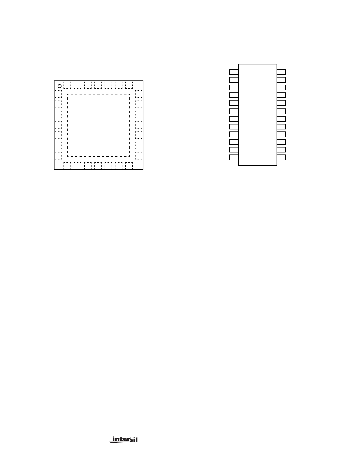
Pinouts
ISL6252, ISL6252A
(28 LD QFN)
TOP VIEW
ISL6252, ISL6252A
ISL6252, ISL6252A
(24 LD QSOP)
TOP VIEW
EN
CELLS
ICOMP
VCOMP
ICM
VREF
CHLIM
ACSET
NA
28 27 26 25 24 23 22
1
2
3
4
5
6
7
8 9 10 11 12 13 14
VADJ
ACLIM
VDD
GND
DCIN
PGND
NA
LGATE
ACPRN
VDDP
CSON
21
20
19
18
17
16
15
BOOT
CSOP
CSIN
CSIP
NA
NA
PHASE
UGATE
VDD
EN
CELLS
ICOMP
VCOMP
ICM
VREF
CHLIM
ACLIM
VADJ LGATE
GND PGND
124
223
322
421
520
619
718
817
916
10 15
11 14
12 13
DCIN
ACPRN ACSET
CSON
CSOP
CSIN
CSIP
PHASE
UGATE
BOOT
VDDP
2
FN6498.1
July 19, 2007
ISL6252, ISL6252A
ICM CSIP CSIN
ACSET
ACPRN
ACLIM
ICOMP
VCOMP
VADJ
CELLS
VREF
VREF
152kΩ
152kΩ
VREF
514kΩ
514kΩ
VOLTAGE
SELECTOR
REFERENCE
VDD
+
-
ADAPTER
CURRENT
LIMIT SET
gm1
+
2.1V
1.26V
-
gm3
+
CURRENT
MIN
VOLTAGE
BUFFER
-
BUFFER
288kΩ
32kΩ
16kΩ
48kΩ
MIN
Σ
-0.25
CA2
X19.9
-
-
+
gm2
X19.9
CA1
+
-
300kHz
RAMP
+
-
PWM
+
LDO
REGULATOR
-
+
DCIN
VDD
BOOT
UGATE
PHASE
VDDP
LGATE
PGND
1.065V
EN
GND
FB
CSON
CSOP
CHLIM
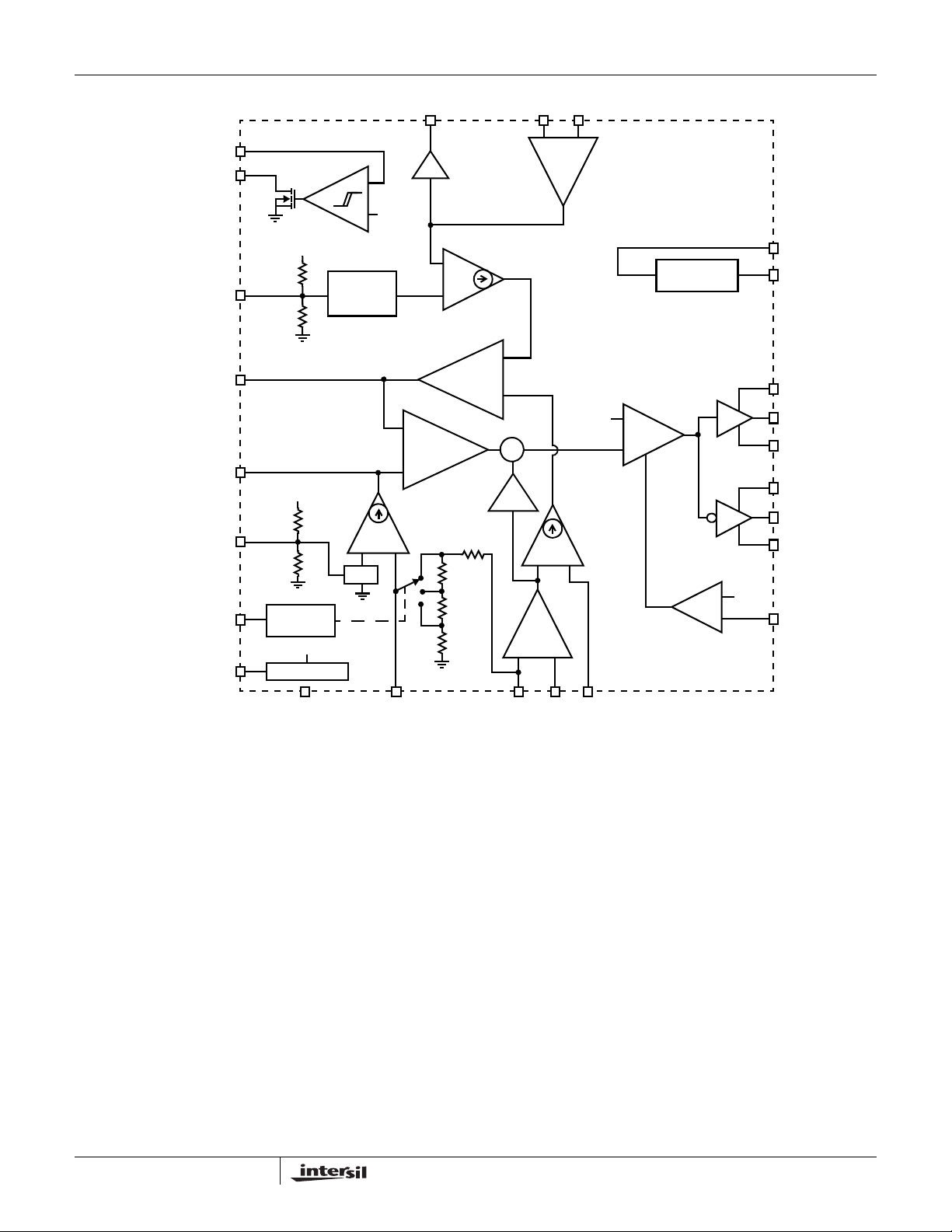
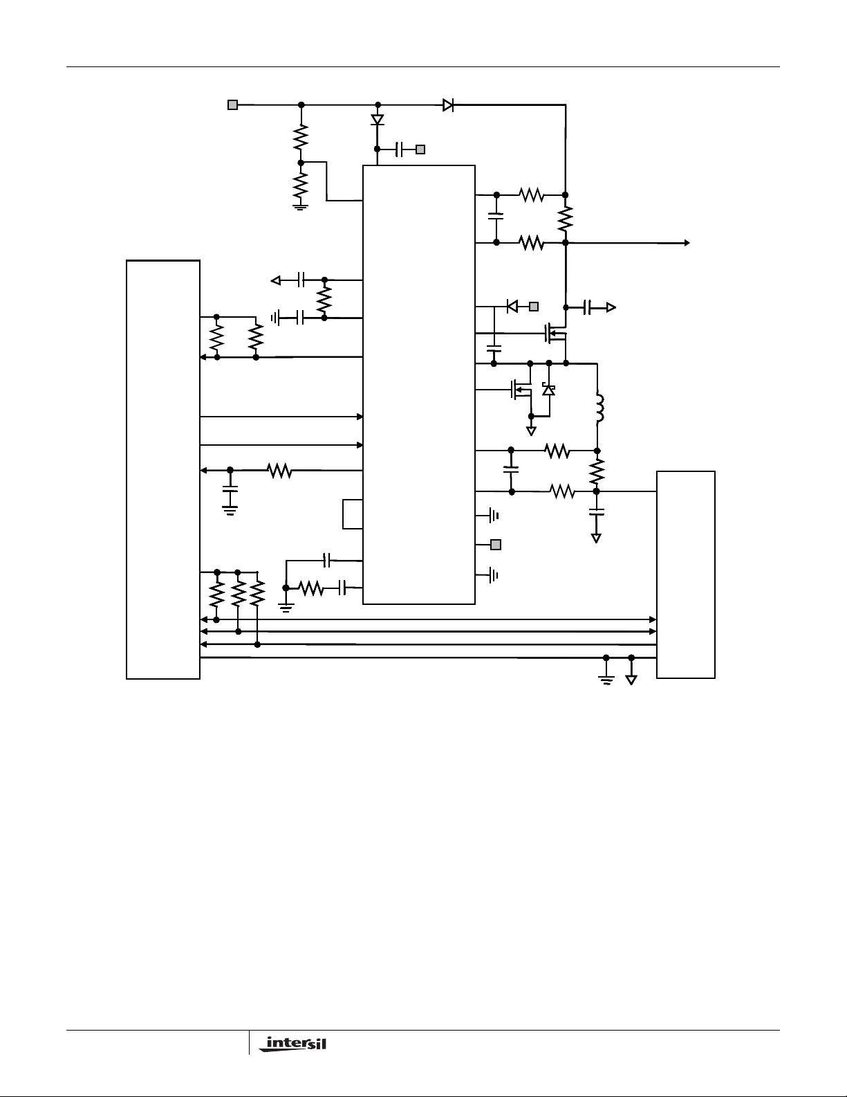
FIGURE 1. FUNCTIONAL BLOCK DIAGRAM
3
FN6498.1
July 19, 2007
TO HOST
CONTROLLER
VREF
VREF
4.7k
CHARGE
CHARGE
CHARGE
CHARGE
ENABLE
ENABLE
ENABLE
ENABLE
R12
R12
2.6A CHARGE LIMIT
2.6A CHARGE LIMIT
20k 1%
20k 1%
253mA TRICKLE CHARGE
1.87k
1.87k
1.87k
1.87k
TRICKLE
TRICKLE
TRICKLE
TRICKLE
CHARGE
CHARGE
CHARGE
CHARGE
AC ADAPTER
R8
R8
R8
R8
130k
130k
130k
130k
1%
1%
1%
1%
R9
R9
R9
R9
10.2k
10.2k
10.2k
10.2k
1%
1%
1%
1%
C7
C7
1µF
1
1
1
3.3V
3.3V
R5
R5
R5
R5
100k
100k
C6
6.8nF
C5
R6
FLOATING
FLOATING
4.2V/CELL
4.2V/CELL
R13
R13
R11
R11
130k
130k
130k
130k
1%
1%
1%
1%
Q6
Q6
Q6
Q6
10nF
1%
1%
1%
1%
R10
R10
R10
R10
4.7
4.7Ω
C9
C9
1µF
1
1
1
ISL6252, ISL6252A
0.1µF
CSON
DCIN
DCIN
DCIN
DCIN
CSIP
CSIP
CSIP
ACSET
ACSET
ACSET
ACSET
IS6252
VDDP
VDDP
VDDP
VDDP
VDD
VDD
VDD
VDD
ACPRN
ACPRN
ACPRN
ACPRN
ICOMP
ICOMP
ICOMP
ICOMP
VCOMP
VCOMP
VCOMP
VCOMP
VADJ
VADJ
VADJ
VADJ
EN
EN
EN
EN
ACLIM
ACLIM
ACLIM
ACLIM
VREF
VREF
VREF
VREF
CHLIM
CHLIM
CHLIM
CHLIM
ISL6252
ISL6252
ISL6252
ISL6252
ISL6252A
ISL
ISL6252
CSIP
CSIN
CSIN
CSIN
CSIN
BOOT
BOOT
BOOT
BOOT
UGATE
UGATE
UGATE
UGATE
PHASE
PHASE
PHASE
PHASE
LGATE
LGATE
LGATE
LGATE
PGND
PGND
PGND
PGND
CSOP
CSOP
CSOP
CSOP
CSON
CSON
CSON
CSON
CELLS
CELLS
CELLS
CELLS
ICM
ICM
ICM
ICM
GND
GND
GND
GND
R7: 100Ω
R21
C2
C2
0.1
0.1
0.1
0.1µF
R22
D2
D2
D2
D2
C4
C4
0.1µF
0.1
0.1
0.1
VDD
VDD
VDD
VDD
4 CELLS
4 CELLS
2.2Ω
22Ω
VDDP
VDDP
VDDP
VDDP
Q2
Q2
R2
R2
R2
R2
20m
20m
20m
20mΩ
Q1
Q1
R11
C3C3
0.047µF
R12
C11
C11
3300pF
3300pF
C1:10
C1:10
D1
D1
D1
D1
OPTIONAL
µ
22Ω
22Ω
SYSTEM LOAD
SYSTEM LOAD
F
F
L
L
L
L
4.7µH
R1
R1
R1
R1
20mΩ
BAT+
BAT+
BAT+
BAT+
C10
C10
22µF
BATTERY
PACK
BAT-
BAT-
BAT-
BAT-
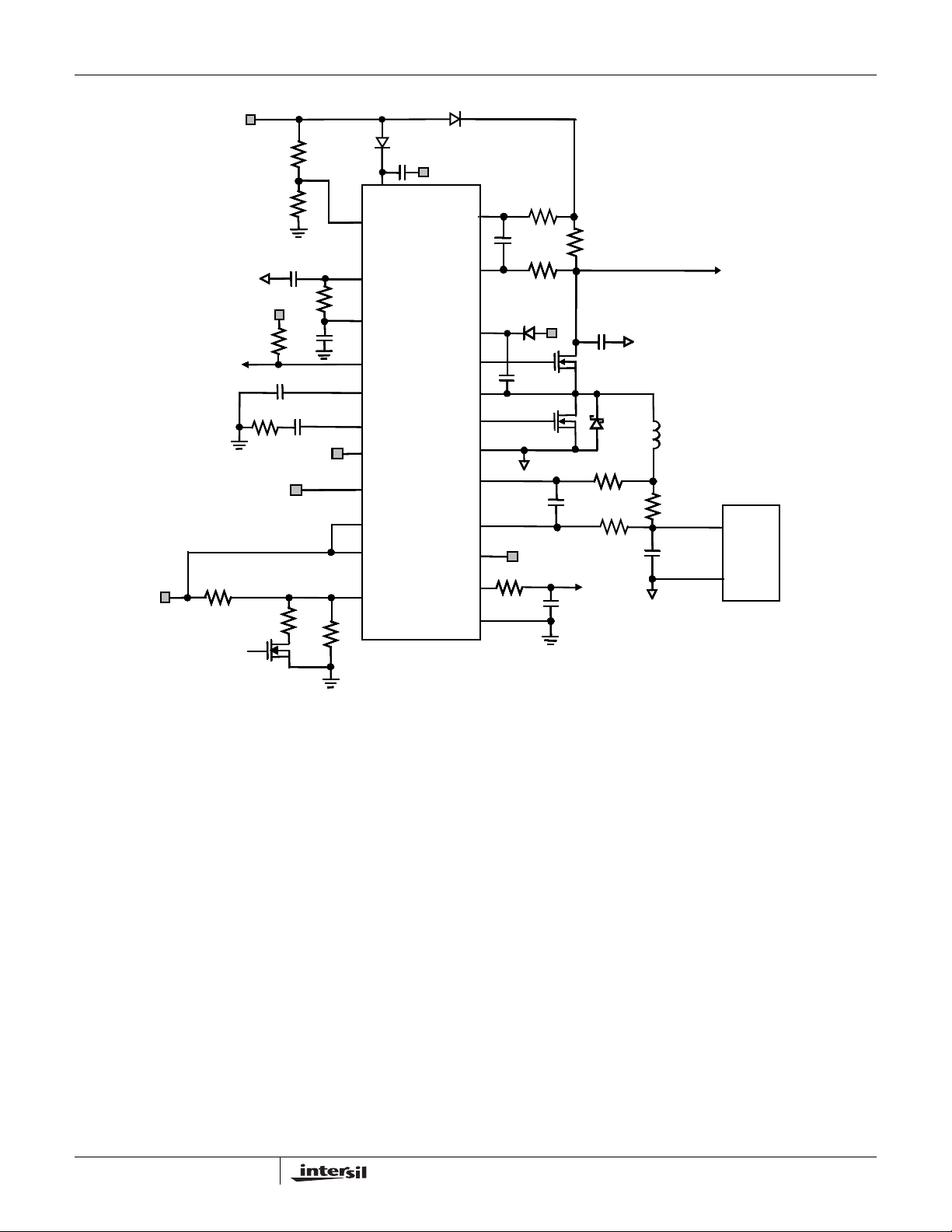
FIGURE 2. ISL6252, ISL6252A TYPICAL APPLICATION CIRCUIT WITH FIXED CHARGING PARAMETERS
4
FN6498.1
July 19, 2007
VCC
VCC
VCC
VCC
DIGITAL
DIGITAL
DIGITAL
DIGITAL
INPUT
INPUT
INPUT
INPUT
D/A OUTPUT
D/A OUTPUT
D/A OUTPUT
D/A OUTPUT
OUTPUT
OUTPUT
OUTPUT
OUTPUT
A/D INPUT
A/D INPUT
A/D INPUT
A/D INPUT
HOST
HOST
HOST
HOST
AVDD/VREF
AVDD/VREF
AVDD/VREF
AVDD/VREF
SCL
SCL
SCL
SCL
SDL
SDL
SDL
SDL
A/D INPUT
A/D INPUT
A/D INPUT
A/D INPUT
GND
GND
GND
GND
ADAPTER
R16
100k
100k
100k
C11
C11
3300pF
3300pF
R11, R12
R13: 10k
R8
R8
R8
R8
130k
130k
130k
130k
1%
1%
1%
1%
R9
R9
R9
R9
10.2k
10.2k
10.2k
10.2k
1%
1%
1%
1%
C7
C7
1
1
µF
C9
C9
1µF
1
R5
R5
R5
R5
100k
100k
100k
R7: 100Ω
R7:
5.15A INPUT
5.15A INPUT
5.15A INPUT
CURRENT LIMIT
CURRENT LIMIT
CURRENT LIMIT
CURRENT LIMIT
R6
R6
R6
R6
4.7k
ISL6252, ISL6252A
C8
C8
0.1µF
0.1
0.1
0.1
CSON
DCIN
DCIN
DCIN
ACSET
ACSET
ACSET
ISL6252
ISL6252
ISL6252
ISL6252A
ISL
ISL6252
VDDP
VDDP
VDDP
R10
R10
4.7
4.7
4.7
4.7Ω
VDD
VDD
C6
C6
6.8nF
6.8nF
6.8nF
6.8nF
C5
C5
10nF
VDD
ACPRN
ACPRN
ACPRN
CHLIM
CHLIM
CHLIM
EN
EN
EN
ICM
ICM
ICM
ACLIM
ACLIM
ACLIM
VREF
VREF
VREF
ICOMP
ICOMP
ICOMP
VCOMP
VCOMP
VCOMP
UGATE
UGATE
PHASE
PHASE
LGATE
LGATE
CSIP
CSIP
CSIP
CSIN
CSIN
CSIN
BOOT
BOOT
BOOT
UGATE
PHASE
LGATE
PGND
PGND
PGND
CSOP
CSOP
CSOP
CSON
CSON
CSON
CELLS
CELLS
CELLS
VADJ
VADJ
VADJ
GND
GND
GND
R21
C2
C2
0.1µF
0.1
0.1
0.1
R22
D2
D2
C4
C4
0.1µF
0.1
0.1
0.1
Q2
Q2
GND
GND
GND
GND
3-CELLS
FLOATING
4.2V/CELL
4.2V/CELL
4.2V/CELL
2.2Ω
22Ω
VDDP
VDDP
R11
C3
C3
0.047µF
R12
R2
R2
R2
R2
20m
20m
20m
20mΩ
C1:10µF
C1:10
C1:10
C1:10
Q1
Q1
Q1
Q1
D1
D1
OPTIONAL
22Ω
22Ω
L
4.7µH
R1
R1
R1
R1
20mΩ
C10
22µF
SYSTEM LOAD
SYSTEM LOAD
BAT+
BAT+
BAT+
BAT+
BATTERY
PACK
SCL
SCL
SCL
SCL
SDL
SDL
SDL
SDL
TEMP
TEMP
TEMP
TEMP
BAT-
BAT-
BAT-
FIGURE 3. ISL6252, ISL6252A TYPICAL APPLICATION CIRCUIT WITH µP CONTROL
5
FN6498.1
July 19, 2007
ISL6252, ISL6252A
Absolute Maximum Ratings Thermal Information
ACSET to GND (Note 3) . . . . . . . . . . . . . . . . . . -0.3V to VDD +0.3V
DCIN, CSIP, CSON to GND. . . . . . . . . . . . . . . . . . . . .-0.3V to +28V
CSIP-CSIN, CSOP-CSON. . . . . . . . . . . . . . . . . . . . . -0.3V to +0.3V
PHASE to GND . . . . . . . . . . . . . . . . . . . . . . . . . . . . . . . . -7V to 30V
BOOT to GND . . . . . . . . . . . . . . . . . . . . . . . . . . . . . . .-0.3V to +35V
BOOT to VDDP . . . . . . . . . . . . . . . . . . . . . . . . . . . . . . . . -2V to 28V
ACLIM, ACPRN, CHLIM, VDD to GND . . . . . . . . . . . . . .-0.3V to 7V
BOOT-PHASE, VDDP-PGND . . . . . . . . . . . . . . . . . . . . . -0.3V to 7V
ICM, ICOMP, VCOMP to GND. . . . . . . . . . . . . . -0.3V to VDD +0.3V
VREF, CELLS to GND . . . . . . . . . . . . . . . . . . . . -0.3V to VDD +0.3V
EN, VADJ, PGND to GND . . . . . . . . . . . . . . . . . -0.3V to VDD +0.3V
UGATE. . . . . . . . . . . . . . . . . . . . . . . . PHASE -0.3V to BOOT +0.3V
LGATE. . . . . . . . . . . . . . . . . . . . . . . . . PGND -0.3V to VDDP +0.3V
CAUTION: Do not operate at or near the maximum ratings listed for extended periods of time. Exposure to such conditions may adversely impact product reliability and
result in failures not covered by warranty.
NOTES:
3. ACSET may be operated 1V below GND if the current through ACSET is limited to less than 1mA.
is measured in free air with the component mounted on a high effective thermal conductivity test board with “direct attach” features. See T ech
4. θ
JA
Brief TB379.
5. For θ
, the “case temp” location is the center of the exposed metal pad on the package underside.
JC
Electrical Specifications DCIN = CSIP = CSIN = 18V, CSOP= CSON = 12V, ACSET = 1.5V, ACLIM = VREF, VADJ= Floating,
EN = VDD = 5V, BOOT-PHASE = 5.0V, GND = PGND = 0V, C
T
≤+125°C, Unless Otherwise Noted.
J
PARAMETER TEST CONDITIONS MIN TYP MAX UNITS
SUPPLY AND BIAS REGULATOR
DCIN Input Voltage Range 7 25 V
DCIN Quiescent Current EN = VDD or GND, 7V ≤ DCIN ≤ 25V 1.4 3 mA
Battery Leakage Current (Note 6) DCIN = 0, no load 3 10 µA
VDD Output Voltage/Regulation 7V ≤ DCIN ≤ 25V, 0 ≤ I
VDD Undervoltage Lockout Trip Point VDD Rising 4.0 4.4 4.6 V
Hysteresis 200 250 400 mV
Reference Output Voltage VREF 0 ≤ I
≤ 300µA 2.365 2.39 2.415 V
VREF
Battery Charge Voltage Accuracy CSON = 16.8V, CELLS= VDD, VADJ = Float -0.5 0.5 %
CSON = 12.6V, CELLS = GND, VADJ = Float -0.5 0.5 %
CSON = 8.4V, CELLS= Float, VADJ = Float -0.5 0.5 %
CSON = 17.64V, CELLS= VDD, VADJ= VREF -0.5 0.5 %
CSON = 13.23V , CELLS = GND, VADJ = VREF -0.5 0.5 %
CSON = 8.82V, CELLS= Float, VADJ= VREF -0.5 0.5 %
CSON = 15.96V, CELLS= VDD, VADJ = GND -0.5 0.5 %
CSON = 11.97V, CELLS = GND, VADJ = GND -0.5 0.5 %
CSON = 7.98V, CELLS = Float, VADJ = GND -0.5 0.5 %
TRIP POINTS
ACSET Threshold 1.24 1.26 1.28 V
ACSET Input Bias Current Hysteresis 2.4 3.4 4.4 µA
ACSET Input Bias Current ACSET ≥ 1.26V 2.4 3.4 4.4 µA
ACSET Input Bias Current ACSET < 1.26V -1 0 1 µA
VDD
Thermal Resistance θ
(°C/W) θJC (°C/W)
JA
QFN Package (Notes 4, 5). . . . . . . . . . 39 9.5
QSOP Package (Note 4) . . . . . . . . . . . 80 NA
Junction Temperature Range. . . . . . . . . . . . . . . . . .-10°C to +150°C
Operating Temperature Range . . . . . . . . . . . . . . . .-10°C to +100°C
Storage Temperature. . . . . . . . . . . . . . . . . . . . . . . .-65°C to +150°C
Pb-free reflow profile . . . . . . . . . . . . . . . . . . . . . . . . . .see link below
http://www.intersil.com/pbfree/Pb-FreeReflow.asp
VDD
=1µF, I
=0mA, TA= -10°C to +100°C,
VDD
≤ 30mA 4.925 5.075 5.225 V
6
FN6498.1
July 19, 2007
ISL6252, ISL6252A
Electrical Specifications DCIN = CSIP = CSIN = 18V, CSOP = CSON = 12V, ACSET = 1.5V, ACLIM = VREF, VADJ = Floating,
EN = VDD = 5V, BOOT-PHASE = 5.0V, GND = PGND = 0V, C
T
≤+125°C, Unless Otherwise Noted. (Continued)
J
PARAMETER TEST CONDITIONS MIN TYP MAX UNITS
OSCILLATOR
Frequency 245 300 355 kHz
PWM Ramp Voltage (peak-peak) CSIP = 18V 1.6 V
CSIP = 11V 1 V
SYNCHRONOUS BUCK REGULATOR
Maximum Duty Cycle 97 99 99.6 %
UGATE Pull-Up Resistance BOOT-PHASE = 5V, 500mA source current 1.8 3.0 Ω
UGATE Source Current BOOT-PHASE= 5V, BOOT-UGATE= 2.5V 1.0 A
UGATE Pull-down Resistance BOOT-PHASE = 5V, 500mA sink current 1.0 1.8 Ω
UGATE Sink Current BOOT-PHASE= 5V, UGATE-PHASE = 2.5V 1.8 A
LGATE Pull-Up Resistance VDDP-PGND = 5V, 500mA source current 1.8 3.0 Ω
LGATE Source Current VDDP-PGND = 5V, VDDP-LGATE = 2.5V 1.0 A
LGATE Pull-Down Resistance VDDP-PGND = 5V, 500mA sink current 1.0 1.8 Ω
LGATE Sink Current VDDP-PGND = 5V, LGATE = 2.5V 1.8 A
Dead Time Falling UGATE to rising LGATE or
CHARGING CURRENT SENSING AMPLIFIER
Input Common-Mode Range 0 18 V
Input Bias Current at CSOP 5 < CSOP < 18V 0.25 2 µA
Input Bias Current at CSON 5 < CSON < 18V 75 100 µA
CHLIM Input Voltage Range 0 3.6 V
ISL6252
CSOP to CSON Full-Scale Current Sense
Voltage
ISL6252A
CSOP to CSON Full-Scale Current Sense
Voltage
ISL6252 CSOP to CSON Full-Scale
Current Sense Voltage formula
ISL6252A CSOP to CSON Full-Scale
Current Sense Voltage formula
CHLIM Input Bias Current CHLIM = GND or 3.3V, DCIN = 0V -1 1 µA
CHLIM Power-Down Mode Threshold
Voltage
CHLIM Power-Down Mode Hysteresis
Voltage
ADAPTER CURRENT SENSING AMPLIFIER
Input Common-Mode Range 7 25 V
Input Bias Current at CSIP and CSIN
Combined
Input Bias Current at CSIN 0 < CSIN < DCIN 0.10 µA
falling LGATE to rising UGATE
ISL6252: CHLIM = 3.3V 160 165 170 mV
ISL6252: CHLIM = 2.0V 95 100 105 mV
ISL6252: CHLIM = 0.2V 5.0 10 15.0 mV
ISL6252A: CHLIM = 3.3V 161.7 165 168.3 mV
ISL6252A: CHLIM = 2.0V 97 100 103 mV
ISL6252A: CHLIM = 0.2V 7.5 10 12.5 mV
Charge current limit mode
0.2V < CHLIM < 3.3V
Charge current limit mode
0.2V < CHLIM < 3.3V
CHLIM rising 80 88 95 mV
CSIP = CSIN = 25V 100 130 µA
CHLIM*49.72
=1µF, I
VDD
10 30 ns
CHLIM*50
-5
-2.4
15 25 40 mV
=0mA, TA= -10°C to +100°C,
VDD
CHLIM*50
+5
CHLIM*50.28
+2.4
mV
mV
7
FN6498.1
July 19, 2007
ISL6252, ISL6252A
Electrical Specifications DCIN = CSIP = CSIN = 18V, CSOP = CSON = 12V, ACSET = 1.5V, ACLIM = VREF, VADJ = Floating,
EN = VDD = 5V, BOOT-PHASE = 5.0V, GND = PGND = 0V, C
T
≤+125°C, Unless Otherwise Noted. (Continued)
J
PARAMETER TEST CONDITIONS MIN TYP MAX UNITS
ADAPTER CURRENT LIMIT THRESHOLD
CSIP to CSIN Full-Scale Current Sense
Voltage
ACLIM = VREF 97 100 103 mV
ACLIM = Float 72 75 78 mV
ACLIM = GND 47 50 53 mV
ACLIM Input Bias Current ACLIM = VREF 10 16 20 µA
ACLIM = GND -20 -16 -10 µA
VOLTAGE REGULATION ERROR AMPLIFIER
Error Amplifier Transconductance from
CELLS = VDD 30 µA/V
CSON to VCOMP
CURRENT REGULATION ERROR AMPLIFIER
Charging Current Error Amplifier
Transconductance
Adapter Current Error Amplifier
Transconductance
BATTERY CELL SELECTOR
CELLS Input Voltage for 4 Cell Select 4.3 V
CELLS Input Voltage for 3 Cell Select 2V
CELLS Input Voltage for 2 Cell Select 2.1 4.2 V
LOGIC INTERFACE
EN Input Voltage Range 0VDDV
EN Threshold Voltage Rising 1.030 1.06 1.100 V
Falling 0.985 1.000 1.025 V
Hysteresis 30 60 90 mV
EN Input Bias Current EN = 2.5V 1.8 2.0 2.2 µA
ACPRN Sink Current ACPRN = 0.4V 3 8 11 mA
ACPRN Leakage Current ACPRN = 5V -0.5 0.5 µA
ICM Output Accuracy
(V
= 19.9 x (V
ICM
CSIP
- V
CSIN
))
CSIP-CSIN = 100mV -3 0 +3 %
CSIP-CSIN = 75mV -4 0 +4 %
CSIP-CSIN = 50mV -5 0 +5 %
Thermal Shutdown Temperature 150 °C
Thermal Shutdown Temperature
Hysteresis
NOTE:
6. This is the sum of currents in these pins (CSIP, CSIN, BOOT, UGATE, PHASE, CSOP, CSON) all tied to 16.8V. No current in pins EN, ACSET,
VADJ, CELLS, ACLIM, CHLIM.
VDD
=1µF, I
=0mA, TA= -10°C to +100°C,
VDD
50 µA/V
50 µA/V
25 °C
8
FN6498.1
July 19, 2007

A
A
ISL6252, ISL6252A
Typical Operating Performance DCIN = 20V, 4S2P Li-Battery, T
0.6
0.3
0.0
-0.3
VDD LOAD REGULATION ACCURACY (%)
-0.6
10
9
8
7
(%)
|
6
5
4
ACCURACY
|
3
2
1
0
150 5 10 20 40
LOAD CURRENT (mA)
FIGURE 4. VDD LOAD REGULATION
0
10 20 30 40 50 60 70 80 90
CSIP-CSIN (mV)
100
VREF LOAD REGULATION ACCURACY (%)
EFFICIENCY (%)
= +25°C, Unless Otherwise Noted.
A
0.10
0.08
0.06
0.04
0.02
0.00
0 100 200 300 400
LOAD CURRENT (μA)
FIGURE 5. VREF LOAD REGULATION
100
96
92
88
84
VCSON = 16.8V
VCSON = 12.6V
3 CELLS
4 CELLS
80
76
1.50 0.5 1.0 2.0 2.5 3.0 3.5 4.0
LOAD CURRENT (A)
VCSON = 8.4V
2 CELLS
FIGURE 6. ACCURACY vs AC ADAPTER CURRENT
DCIN
DCIN
10V/div
10V/div
ACSET
ACSET
1V/div
1V/div
DCSET
DCSET
1V/div
1V/div
DCPRN
DCPRN
5V/div
5V/div
ACPRN
ACPRN
5V/div
5V/div
FIGURE 8. AC AND DC ADAPTER DETECTION
9
FIGURE 7. SYSTEM EFFICIENCY vs CHARGE CURRENT
LOAD
CURRENT
5A/div
DAPTER
CURRENT
5A/div
CHARGE
CURRENT
2A/div
LOAD STEP: 0A TO 4A
LOAD STEP: 0-4A
CHARGE CURRENT: 3A
CHARGE CURRENT: 3A
AC ADAPTER CURRENT LIMIT: 5.15A
C ADAPTER CURRENT LIMIT: 5.15A
BATTERY
VOLTAGE
2V/div
FIGURE 9. LOAD TRANSIENT RESPONSE
FN6498.1
July 19, 2007

P
P
P
P
P
P
ISL6252, ISL6252A
Typical Operating Performance DCIN = 20V, 4S2P Li-Battery, T
CSON
CSON
5V/div
5V/div
EN
EN
5V/div
5V/div
INDUCTOR
INDUCTOR
CURRENT
CURRENT
2A/div
2A/div
CHARGE
CHARGE
CURRENT
CURRENT
2A/div
2A/div
FIGURE 10. CHARGE ENABLE AND SHUTDOWN
CHLIM = 0.2V
CHLIM=0.2V
CHLIM=0.2V
CSON = 8V
CSON=8V
CSON=8V
PHASE
PHASE
PHASE
10V/div
10V/div
10V/div
INDUCTOR
INDUCTOR
INDUCTOR
CURRENT
CURRENT
CURRENT
1A/div
1A/div
1A/div
= +25°C, Unless Otherwise Noted. (Continued)
A
INDUCTOR
INDUCTOR
CURRENT
CURRENT
2A/div
2A/div
BATTERY
BATTERY
BATTERY
REMOVAL
REMOVAL
REMOVAL
CSON
CSON
10V/div
10V/div
VCOMP
VCOMP
2V/div
2V/div
ICOMP
ICOMP
2V/div
2V/div
VCOMP
VCOMP
VCOMP
ICOMP
ICOMP
ICOMP
BATTERY
BATTERY
BATTERY
INSERTION
INSERTION
INSERTION
FIGURE 11. BATTERY INSERTION AND REMOVAL
PHASE
PHASE
10V/div
10V/div
UGATE
UGATE
2V/div
2V/div
UGATE
UGATE
UGATE
5V/div
5V/div
5V/div
LGATE
LGATE
2V/div
2V/div
FIGURE 12. AC ADAPTER REMOVAL FIGURE 13. AC ADAPTER INSERTION
BGATE-CSI
BGATE-CSI
ADAPTER REMOVAL
ADAPTER REMOVAL
ADAPTER REMOVAL
SGATE-CSIP
SGATE-CSIP
SGATE-CSIP
2V/div
2V/div
2V/div
SYSTEM BUS
SYSTEM BUS
SYSTEM BUS
VOLTAGE
VOLTAGE
VOLTAGE
10V/div
10V/div
10V/div
BGATE-CSIP
BGATE-CSIP
BGATE-CSIP
2V/div
2V/div
2V/div
INDUCTOR
INDUCTOR
INDUCTOR
CURRENT
CURRENT
CURRENT
2A/div
2A/div
2A/div
ADAPTER INSERTION
ADAPTER INSERTION
ADAPTER INSERTION
BGATE-CSI
2V/div
2V/div
2V/div
SYSTEM BU
SYSTEM BU
SYSTEM BU
VOLTAGE
VOLTAGE
VOLTAGE
10V/div
10V/div
10V/div
SGATE-CSI
SGATE-CSI
SGATE-CSI
2V/div
2V/div
2V/div
INDUCTOR
INDUCTOR
INDUCTOR
CURRENT
CURRENT
CURRENT
2A/div
2A/div
2A/div
FIGURE 14. SWITCHING WA VEFORMS A T DIODE EMULA TION FIGURE 15. SWITCHING WAVEFORMS IN CC MODE
10
FN6498.1
July 19, 2007

ISL6252, ISL6252A
Typical Operating Performance DCIN = 20V, 4S2P Li-Battery, T
FIGURE 16. TRICKLE TO FULL-SCALE CHARGING
Functional Pin Descriptions
BOOT
Connect BOOT to a 0.1µF ceramic capacitor to PHASE pin
and connect to the cathode of the bootstrap Schottky diode.
UGATE
UGATE is the high side MOSFET gate drive output.
LGATE
LGATE is the low side MOSFET gate drive output; swing
between 0V and VDDP.
PHASE
The Phase connection pin connects to the high side
MOSFET source, output inductor, and low side MOSFET
drain.
CSOP/CSON
CSOP/CSON is the battery charging current sensing
positive/negative input. The differential voltage across CSOP
and CSON is used to sense the battery charging current,
and is compared with the charging current limit threshold to
regulate the charging current. The CSON pin is also used as
the battery feedback voltage to perform voltage regulation.
CSIP/CSIN
CSIP/CSIN is the AC adapter current sensing
positive/negative input. The differential voltage across CSIP
and CSIN is used to sense the AC adapter current, and is
compared with the AC adapter current limit to regulate the
AC adapter current.
GND
GND is an analog ground.
DCIN
The DCIN pin is the input of the internal 5V LDO. Connect it
to the AC adapter output. Connect a 0.1µF ceramic
capacitor from DCIN to CSON.
ACSET
ACSET is an AC adapter detection input. Connect to a
resistor divider from the AC adapter output.
ACPRN
Open-drain output signals AC adapter is present. ACPRN
pulls low when ACSET is higher than 1.26V; and pulled high
when ACSET is lower than 1.26V.
EN
EN is the Charge Enable input. Connecting EN to high
enables the charge control function, connecting EN to low
disables charging functions. Use with a thermistor to detect
a hot battery and suspend charging.
ICM
ICM is the adapter current output. The output of this pin
produces a voltage proportional to the adapter current.
PGND
PGND is the power ground. Connect PGND to the source of
the low side MOSFET.
VDD
VDD is an internal LDO output to supply IC analog circuit.
Connect a 1μF ceramic capacitor to ground.
VDDP
VDDP is the supply voltage for the low-side MOSFET gate
driver. Connect a 4.7Ω resistor to VDD and a 1μF ceramic
capacitor to power ground.
ICOMP
ICOMP is a current loop error amplifier output.
VCOMP
VCOMP is a voltage loop amplifier output.
CELLS
This pin is used to select the battery voltage. CELLS = VDD
for a 4S battery pack, CELLS = GND for a 3S battery pack,
CELLS = Float for a 2S battery pack.
= +25°C, Unless Otherwise Noted. (Continued)
A
CHARGE
CURRENT
1A/div
CHLIM
1V/div
11
FN6498.1
July 19, 2007

ISL6252, ISL6252A
VADJ
VADJ adjust s battery regulation voltage. VADJ = VREF for
4.2V+5%/cell; VADJ = Floating for 4.2V/cell; VADJ = GND
for 4.2V-5%/cell. Connect to a resistor divider to program the
desired battery cell voltage between 4.2V-5% and 4.2V+5%.
CHLIM
CHLIM is the battery charge current limit set pin. CHLIM
input voltage range is 0.1V to 3.6V. When CHLIM = 3.3V, the
set point for CSOP to CSON is 165mV. The charger shuts
down if CHLIM is forced below 88mV.
ACLIM
ACLIM is the adapter current limit set pin. ACLIM = VREF for
100mV, ACLIM = Floating for 75mV, and ACLIM = GND for
50mV. Connect a resistor divider to program the adapter
current limit threshold between 50mV and 100mV.
VREF
VREF is a 2.39V reference output pin. It is internally
compensated. Do not connect a decoupling capacitor.
Theory of Operation
Introduction
Unless otherwise noted, all descriptions of ISL6252 refer to
both ISL6252 and ISL6252A. The ISL6252 includes all of the
functions necessary to charge 2 to 4 cell Li-Ion and Lipolymer batteries. A high efficiency synchronous buck
converter is used to control the charging voltage and
charging current up to 10A. The ISL6252 has input current
limiting and analog inputs for setting the charge current and
charge voltage; CHLIM inputs are used to control charge
current and VADJ inputs are used to control charge voltage.
The ISL6252 charges the battery with constant charge
current, set by CHLIM input, until the battery voltage rises up
to a programmed charge voltage set by VADJ input; then the
charger begins to operate at a constant voltage charge mode.
The charger also drives an adapter isolation P-Channel
MOSFET to efficiently switch in the adapter supply.
ISL6252 is a complete power source selection controller for
single battery systems and also aircraft power applications.
It drives a battery selector P-Channel MOSFET to efficiently
select between a single battery and the adapter. It controls
the battery discharging MOSFET and switches to the battery
when the AC adapter is removed, or, switches to the AC
adapter when the AC adapter is inserted for single battery
system.
The EN input allows shutdown of the charger through a
command from a micro-controller. It also uses EN to safely
shutdown the charger when the battery is in extremely hot
conditions. The amount of adapter current is reported on the
ICM output. Figure 1 shows the IC functional block diagram.
The synchronous buck converter uses external N-Channel
MOSFETs to convert the input voltage to the required
charging current and charging voltage. Figure 2 shows the
ISL6252 typical application circuit with charging current and
charging voltage fixed at specific values. The typical
application circuit shown in Figure 3 shows the ISL6252
typical application circuit which uses a micro-controller to
adjust the charging current set by CHLIM input for aircraft
power applications. The voltage at CHLIM and the valu e of R
sets the charging current. The DC/DC converter generates
the control signals to drive two external N-Channel MOSFETs
to regulate the voltage and current set by the ACLIM, CHLIM,
V ADJ and CELLS input s.
The ISL6252 features a voltage regulation loop (VCOMP)
and two current regulation loops (ICOMP). The VCOMP
voltage regulation loop monitors CSON to ensure that its
voltage never exceeds the voltage and regulates the battery
charge voltage set by VADJ. The ICOMP current regulation
loops regulate the battery charging current delivered to the
battery to ensure that it never exceeds the charging current
limit set by CHLIM; and the ICOMP current regulation loops
also regulate the input current drawn from the AC adapter to
ensure that it never exceeds the input current limit set by
ACLIM, and to prevent a system crash and AC adapter
overload.
PWM Control
The ISL6252 employs a fixed frequency PWM current mode
control architecture with a feed -forward function. The
feed-forward function maintains a constant modulator gain of
11 to achieve fast line regulation as the buck input voltage
changes. When the battery charge voltage approaches the
input voltage, the DC/DC converter operates in dropout
mode, where there is a timer to prevent the frequency from
dropping into the audible frequency range. It can achieve
duty cycle of up to 99.6%.
To prevent boosting of the system bus voltage, the battery
charger operates in standard-buck mode when CSOPCSON drops below 4.25mV. Once in standard-buck mode,
hysteresis does not allow synchronous operation of the
DC/DC converter until CSOP-CSON rises above 12.5mV.
An adaptive gate drive scheme is used to control the dead
time between two switches. The dead time control circuit
monitors the LGATE output and prevents the upper side
MOSFET from turning on until LGATE is fully off, preventing
cross-conduction and shoot-through. In order for the dead
time circuit to work properly, there must be a low resistance,
low inductance path from the LGATE driver to MOSFET
gate, and from the source of MOSFET to PGND. The
external Schottky diode is between the VDDP pin and BOOT
pin to keep the bootstrap capacitor charged.
Setting the Battery Regulation Voltage
The ISL6252 uses a high-accuracy trimmed band-gap
voltage reference to regulate the battery charging voltage.
The VADJ input adjusts the charger output voltage, and the
VADJ control voltage can vary from 0 to VREF, providing a
1
12
FN6498.1
July 19, 2007

ISL6252, ISL6252A
10% adjustment range (from 4.2V-5% to 4.2V+5%) on
CSON regulation voltage. An overall voltage accuracy of
better than 0.5% is achieved.
The per-cell battery termination voltage is a function of the
battery chemistry. Consult the battery manufacturers to
determine this voltage.
• Float VADJ to set the battery voltage
V
=4.2V × number of the cells,
CSON
• Connect VADJ to VREF to set 4.41V × number of cells,
• Connect VADJ to ground to set 3.99V × number of cells.
So, the maximum battery voltage of 17.6V can be achieved.
Note that other battery charge voltages can be set by
connecting a resistor divider from VREF to ground. The resistor
divider should be sized to draw no more than 100µA from
VREF; or connect a low impedance voltage source like the D/A
converter in the micro-controller. The programmed battery
voltage per cell can be determined by Equation 1:
V
CELL
0.175 V
⋅ 3.99V+=
VADJ
(EQ. 1)
An external resistor divider from VREF sets the voltage at
V A D J according to Equation 2:
V
VADJ
=
VREF
R
-----------------------------------------------------------------------------------------------------------------
×
R
top_VADJ
bot_VADJ
514kΩ||R
||
+
514kΩ
bot_VADJ
||
514kΩ
(EQ. 2)
To minimize accuracy loss due to interaction with VADJ's
internal resistor divider, ensure the AC resistance looking
back into the external resistor divider is less than 25k.
Connect CELLS as shown in Table 1 to charge 2, 3 or 4 Li+
cells. When charging other cell chemistries, use CELLS to
select an output voltage range for the charger. The internal
error amplifier gm1 maintains voltage regulation. The voltage
error amplifier is compensated at VCOMP. The component
values shown in Figure 3 provide suitable performance for most
applications. Individual compensation of the voltage regulation
and current-regulation loops allows for optimal compensation.
TABLE 1. CELL NUMBER PROGRAMMING
CELLS CELL NUMBER
VDD 4
GND 3
Float 2
Setting the Battery Charge Current Limit
The CHLIM input sets the maximum charging current. The
current set by the current sense-resistor connects between
CSOP and CSON. The full-scale differential voltage between
CSOP and CSON is 165mV for CHLIM = 3.3V, so the
maximum charging current is 4.125A for a 40mΩ sensing
resistor. Other battery charge current-sense threshold
values can be set by connecting a resistor divider from
VREF or 3.3V to ground, or by connecting a low impedance
voltage source like a D/A converter in the micro-controller.
Unlike VADJ and ACLIM, CHLIM does not have an internal
resistor divider network. The charge current limit threshold is
given by Equation 3:
I
CHG
165mV
⎛⎞
-------------------
=
⎝⎠
V
CHLIM
⎛⎞
--------------------- -
⎝⎠
R
3.3V
1
(EQ. 3)
To set the trickle charge current for the dumb charger, an
A/D output controlled by the micro-controller is connected to
CHLIM pin. The trickle charge current is determined by
Equation 4:
I
CHG
165mV
⎛⎞
-------------------
=
⎝⎠
V
CHLIM trickle,
⎛⎞
--------------------------------------- -
⎝⎠
R
1
3.3V
(EQ. 4)
When the CHLIM voltage is below 88mV (typical), it will
disable the battery charge. When choosing the current
sensing resistor, note that the voltage drop across the
sensing resistor causes further power dissipation, reducing
efficiency. However, adjusting CHLIM voltage to reduce the
voltage across the current sense resistor R
will degrade
1
accuracy due to the smaller signal to the input of the current
sense amplifier. There is a trade-off between accuracy and
power dissipation. A low pass filter is recommended to
eliminate switching noise. Connect the resistor to the CSOP
pin instead of the CSON pin, as the CSOP pin has lower
bias current and less influence on current-sense accuracy
and voltage regulation accuracy.
Charge Current Limit Accuracy
The “Electrical Specifications” table on page 6 gives
minimum and maximum values for the CSOP-CSON voltage
resulting from IC variations at 3 different CHLIM voltages
(CSOP-CSON Full-Scale Current Sense Voltage on page7).
It also gives formulae for calculating the minimum and
maximum CSOP-CSON voltage at any CHLIM voltage.
Equation 5 shows the formula for the max full scale
CSOP-CSON voltage (in mV) for the ISL6252A:
ISL6252A
CSOP CSON–()
CSOP CSON–()
Equation 5 shows the formula for the max full scale
CSOP-CSON voltage (in mV) for the ISL6252:
ISL6252
MAX CSOP CSON–()CHLIM 50 5+•=
MIN CSOP CSON–()CHLIM 50 5–•=
With CHLIM = 1.5V, the maximum CSOP-CSON voltage is
78mV and the minimum CSOP-CSON voltage is 72mV.
When ISL6252A is in charge current limiting mode, the
maximum charge current is the maximum CSOP-CSON
MAX
MIN
CHLIM 50 .28 2.4+•=
CHLIM 49.7 2 2.4–•=
(EQ. 5)
(EQ. 6)
13
FN6498.1
July 19, 2007

ISL6252, ISL6252A
voltage divided by the minimum sense resistor. This can be
calculated for ISL6252A with Equation 7:
ISL6252A
I
CHG MAX,
I
CHG MIN,
CHLIM 50.28 2.4+•()R
CHLIM 4 9.72 2.4–•()R
⁄=
⁄=
1MIN
1MAX
(EQ. 7)
Maximum charge current can be calculated for ISL6252 with
Equation 8:
ISL6252
I
CHG MAX,
I
CHG MIN,
With CHLIM = 0.7V and R
I
CHG MAX,
I
CHG MIN,
CHLIM 50 5+•()R
CHLIM 50 5–•()R
ISL6252A
1.5V 50.28 2.4+•()0.0198 3930mA=⁄=
1.5V 49.72 2.4–•()0.0202 3573mA=⁄=
⁄=
= 0.02Ω, 1%:
1
⁄=
1MAX
1MIN
(EQ. 8)
(EQ. 9)
Setting the Input Current Limit
The total input current from an AC adapter, or other DC
source, is a function of the system supply current and the
battery-charging current. The input current regulator limits
the input current by reducing the charging current, when the
input current exceeds the input current limit set point.
System current normally fluctuates as portions of the system
are powered up or down. Without input current regulation,
the source must be able to supply the maximum system
current and the maximum charger input current
simultaneously . By using the input current limiter , the current
capability of the AC adapter can be lowered, reducing
system cost.
The ISL6252 limits the battery charge current when the input
current-limit threshold is exceeded, ensuring the battery
charger does not load down the AC adapter voltage. This
constant input current regulation allows the adapter to fully
power the system and prevent the AC adapter from
overloading and crashing the system bus.
An internal amplifier gm3 compares the voltage between
CSIP and CSIN to the input current limit threshold voltage
set by ACLIM. Connect ACLIM to REF, Float and GND for
the full-scale input current limit threshold voltage of 100mV,
75mV and 50mV, respectively, or use a resistor divider from
VREF to ground to set the input current limit as Equation 10:
0.05
1
⎛⎞
-------
I
INPUT
-----------------
VREF
V
ACLIM
⋅=
⎝⎠
R
2
An external resistor divider from VREF sets the voltage at
ACLIM according to Equation 11:
⎛⎞
V
ACLIM
VREF
------------------------------------------------------------------------------------------------------------------------
⋅=
⎜⎟
R
⎝⎠
top ACLIM,
0.05+⋅
R
bot ACLIM,
152kΩ||R
+
||
152kΩ
bot ACLIM,
(EQ. 10)
||
152kΩ
(EQ. 11)
where R
bot_ACLIM
and R
top_ACLIM
are external resistors at
ACLIM.
To minimize accuracy loss due to interaction with ACLIM's
internal resistor divider, ensure the AC resistance looking
back into the resistor divider is less than 25k.
When choosing the current sense resistor, note that the
voltage drop across this resistor causes further power
dissipation, reducing efficiency. The AC adapter current
sense accuracy is very important. Use a 1% tolerance
current-sense resistor. The highest accuracy of ±3% is
achieved with 100mV current-sense threshold voltage for
ACLIM = VREF, but it has the highest power dissipation. For
example, it has 400mW power dissipation for rated 4A AC
adapter and 1Ω sensing resistor may have to be used. ±4%
and ±6% accuracy can be achieved with 75mV and 50mV
current-sense threshold voltage for ACLIM = Floating and
ACLIM = GND, respectively.
A low pass filter is suggested to eliminate the switching
noise. Connect the resistor to CSIN pin instead of CSIP pin
because CSIN pin has lower bias current and less influence
on the current-sense accuracy.
AC Adapter Detection
Connect the AC adapter voltage through a resistor divider to
ACSET to detect when AC power is available, as shown in
Figure 2. ACPRN is an open-drain output and is high when
ACSET is less than V
above V
th,fall
. V
th,rise
, and active low when ACSET is
th,rise
and V
are given by Equation 12
th,fall
and Equation 13:
R
⎛⎞
8
-------
⋅=
V
th rise,
V
th fall,
1+
⎜⎟
R
⎝⎠
R
⎛⎞
-------
⎜⎟
R
⎝⎠
V
9
8
9
ACSET
1+
V
ACSETIhysR8
⋅–⋅=
(EQ. 12)
(EQ. 13)
where:
•I
is the ACSET input bias current hysteresis, and
hys
•V
The hysteresis is I
= 1.24V (min), 1.26V (typ) and 1.28V (max).
ACSET
hysR8
, where I
= 2.2µA (min),
hys
3.4µA (typ) and 4.4µA (max).
Current Measurement
Use ICM to monitor the input current being sensed across
CSIP and CSIN. The output voltage range is 0V to 2.5V . The
voltage of ICM is proportional to the voltage drop across
CSIP and CSIN, and is given by Equation 14:
ICM 19.9 I
where I
INPUT
ICM has ±3% accuracy. It is recommended to have an RC
filter at the ICM output for minimizing the switching noise.
••=
INPUTR2
(EQ. 14)
is the DC current drawn from the AC adapter.
14
FN6498.1
July 19, 2007

ISL6252, ISL6252A
LDO Regulator
VDD provides a 5.0V supply voltage from the internal LDO
regulator from DCIN and can deliver up to 30mA of current.
The MOSFET drivers are powered by VDDP, which must be
connected to VDDP as shown in Figure 2. VDDP connects
to VDD through an external low pass filter. Bypass VDDP
and VDD with a 1µF capacitor.
Shutdown
The ISL6252 features a low-power shutdown mode. Driving
EN low shuts down the ISL6252. In shutdown, the DC/DC
converter is disabled, and VCOMP and ICOMP are pulled to
ground. The ICM, ACPRN output continue to function.
EN can be driven by a thermistor to allow automatic
shutdown of the ISL6252 when the battery pack is hot. Often
a NTC thermistor is included inside the battery pack to
measure its temperature. When connected to the charger,
the thermistor forms a voltage divider with a resistive pull-up
to the VREF. The threshold voltage of EN is 1.0V with 60mV
hysteresis. The thermistor can be selected to have a
resistance vs temperature characteristic that abruptly
decreases above a critical temperature. This arrangement
automatically shuts down the ISL6252 when the battery pack
is above a critical temperature.
There is a delay of approximately 400nsec between V
OUT
exceeding the OVP trip point and pulling VCOMP, LGATE
and UGATE low.
VCOMP
ICOMP
BATTERY
REMOVAL
PHASE
FIGURE 17. OVERVOLTAGE PROTECTION IN ISL6252
V
OUT
WHEN V
THE OVP THRESHOLD
VCOMP IS PULLED LOW
AND FETS TURN OFF
CURRENT FLOWS IN THE
LOWER FET BODY DIODE
UNTIL INDUCTOR CURRENT
REACHES ZERO
EXCEEDS
OUT
Another method for inhibiting charging is to force CHLIM
below 85mV (typ).
Short Circuit Protection and 0V Battery Charging
Since the battery charger will regulate the charge current to
the limit set by CHLIM, it automatically has short circuit
protection and is able to provide the charge current to wake
up an extremely discharged battery.
Over-Temperature Protection
If the die temp exceeds +150°C, it stops charging. Once the
die temp drops below +125°C, charging will start up again.
Overvoltage Protection
ISL6252 has an Overvoltage Protection circuit that limits the
output voltage when the battery is removed or disconnected
by a pulse charging circuit. If CSON exceeds the output
voltage set point by more than V
pulls VCOMP down and turns off both upper and lower FET s
of the buck as in Figure 17. The trip point for Overvoltage
Protection is always above the nominal output voltage and
can be calculated from Equation 15:
V
OVPVOUT NOM,
N
CELLS
For example, if the CELLS pin is connected to ground
(N
V
OUT,NOM
V
OUT,NOM
CELLS
= 3) and V
ADJ
= 12.6V and V
+93mV.
is floating (V
OVP
an internal comparator
OVP
V
⎛⎞
42.2mV 22.2mV
×+=
⎝⎠
= 1.195V) then
ADJ
ADJ
--------------- -
×–
2.39V
(EQ. 15)
=12.693V or
Application Information
The following battery charger design refers to the typical
application circuit in Figure 2, where typical battery
configuration of 4S2P is used. This section describes how to
select the external components including the inductor, input
and output capacitors, switching MOSFETs, and current
sensing resistors.
Inductor Selection
The inductor selection has trade-offs between cost, size,
cross over frequency and efficiency. For example, the lower
the inductance, the smaller the size, but ripple current is
higher. This also results in higher AC losses in the magnetic
core and the windings, which decrease the system
efficiency. On the other hand, the higher inductance results
in lower ripple current and smaller output filter capacitors,
but it has higher DCR (DC resistance of the inductor) loss,
lower saturation current and has slower transient response.
So, the practical inductor design is based on the inductor
ripple current being ±15% to ±20% of the maximum
operating DC current at maximum input voltage. Maximum
ripple is at 50% duty cycle or V
BAT=VIN,MAX
required inductance can be calculated from Equation 16:
V
IN MAX,
---------------------------------------------
L
=
4fSWI
⋅⋅
RIPPLE
Where V
and fSW are the maximum input voltage,
IN,MAX
and switching frequency, respectively.
/2. The
(EQ. 16)
15
FN6498.1
July 19, 2007

ISL6252, ISL6252A
The inductor ripple current ΔI is found from Equation 17:
I
RIPPLE
0.3 I⋅
=
LMAX,
(EQ. 17)
where the maximum peak-to-peak ripple current is 30% of
the maximum charge current is used.
For V
f
= 300kHz, the calculated indu ctance is 8.3µH. Choosing
s
IN,MAX
= 19V, V
= 16.8V, I
BAT
BAT,MAX
= 2.6A, and
the closest standard value gives L = 10µH. Ferrite cores are
often the best choice since they are optimized at 300kHz to
600kHz operation with low core loss. The core must be large
enough not to saturate at the peak inductor current I
Peak
in
Equation 18:
1
I
PEAKILMAX,
-- -
+ I
2
⋅=
RIPPLE
(EQ. 18)
Inductor saturation can lead to cascade failures due to very
high currents. Conservative design limits the peak and RMS
current in the inductor to less than 90% of the rated
saturation current.
Cross over frequency is heavily dependant on the inductor
value. f
frequency and a conservative design has f
of the switching frequency. The highest f
should be less than 20% of the switching
CO
CO
is in voltage
CO
less than 10%
control mode with the battery removed and may be
calculated (approximately) from Equation 19:
511R
f
CO
=
⋅⋅
------------------------------------------ -
SENSE
2π L⋅
(EQ. 19)
Output Capacitor Selection
The output capacitor in parallel with the battery is used to
absorb the high frequency switching ripple current and
smooth the output voltage. The RMS value of the output
ripple current I
V
RMS
-----------------------------------
12LF
I
where the duty cycle D is the ratio of the output voltage
(battery voltage) over the input voltage for continuous
conduction mode which is typical operation for the battery
charger . During t he batter y charge pe riod, the output vol tage
varies from its initial battery voltage to the rated battery
voltage. So, the duty cycle change can be in the range of
between 0.53 and 0.88 for the minimum battery voltage of
10V (2.5V/Cell) and the maximum battery voltage of 16.8V.
The maximum RMS value of the output ripple current occurs
at the duty cycle of 0.5 and is expressed as Equation 21:
-----------------------------------------
=
I
RMS
4 12Lf
⋅⋅⋅
For V
IN,MAX
f
= 300kHz, the maximum RMS current is 0.19A. A typical
s
10F ceramic capacitor is a good choice to absorb this
current and also has very small size. Organic polymer
capacitors have high capacitance with small size and have a
significant equivalent series resistance (ESR). Although
is given by Equation 20:
rms
IN MAX,
⋅⋅
V
IN MAX,
D1D–()⋅⋅=
SW
SW
= 19V, VBAT = 16.8V, L = 10µH, and
(EQ. 20)
(EQ. 21)
ESR adds to ripple voltage, it also creates a high frequency
zero that helps the closed loop operation of the buck
regulator.
EMI considerations usually make it desirable to minimize
ripple current in the battery leads. Beads may be added in
series with the battery pack to increase the battery
impedance at 300kHz switching frequency. Switching ripple
current splits between the battery and the output capacitor
depending on the ESR of the output capacitor and battery
impedance. If the ESR of the output capacitor is 10mΩ and
battery impedance is raised to 2Ω with a bead, then only
0.5% of the ripple current will flow in the battery.
MOSFET Selection
The Notebook battery charger synchronous buck converter
has the input voltage from the AC adapter output. The
maximum AC adapter output voltage does not exceed 25V.
Therefore, 30V logic MOSFET should be used.
The high side MOSFET must be able to dissipate the
conduction losses plus the switching losses. For the battery
charger application, the input voltage of the synchronous
buck converter is equal to the AC adapter output voltage,
which is relatively constant. The maximum efficiency is
achieved by selecting a high side MOSFET that has the
conduction losses equal to the switching losses. Switching
losses in the low-side FET are very small. The choice of
low-side FET is a trade off between conduction losses
(r
the low-side FET is 2X the r
The LGATE gate driver can drive sufficient gate current to
switch most MOSFETs efficiently . However, some FETs may
exhibit cross conduction (or shoot through) due to current
injected into the drain-to-source parasitic capacitor (C
the high dV/dt rising edge at the phase node when the highside MOSFET turns on. Although LGATE sink current (1.8A
typical) is more than enough to switch the FET off quickly,
voltage drops across parasitic impedances between LGATE
and the MOSFET can allow the gate to rise during the fast
rising edge of voltage on the drain. MOSFETs with low
threshold voltage (<1.5V) and low ratio of C
high gate resistance (>4Ω) may be turned on for a few ns by
the high dV/dt (rising edge) on their drain. This can be
avoided with higher threshold voltage and C
Another way to avoid cross conduction is slowing the turn-on
speed of the high-side MOSFET by connecting a resistor
between the BOOT pin and the boot strap cap.
For the high-side MOSFET, the worst-case conduction
losses occur at the minimum input voltage as shown in
Equation 22:
P
The optimum efficiency occurs when the switching losses
equal the conduction losses. However, it is difficult to
) and cost. A good rule of thumb for the r
DS(ON)
DS(ON)
Q1 conduction,
V
OUT
--------------- -
V
IN
⋅⋅=
I
BAT
2
r
DS ON()
of the high-side FET.
DS(ON)
gd
(<5) and
gs/Cgd
ratio.
gs/Cgd
(EQ. 22)
of
) by
16
FN6498.1
July 19, 2007

ISL6252, ISL6252A
calculate the switching losses in the high-side MOSFET
since it must allow for difficult-to-quantify factors that
influence the turn-on and turn-off times. These factors
include the MOSFET internal gate resistance, gate charge,
threshold voltage, stray inductance, pull-up and pull-down
resistance of the gate driver.
The following switching loss calculation (Equation 23)
provides a rough estimate.
P
Q1 Switching,
1
-- -
V
INILVfsw
2
=
Q
⎛⎞
------------------------ -
⎜⎟
I
⎝⎠
gsource,
gd
1
-- -
V
INILPfsw
2
Q
⎛⎞
gd
-----------------
⎜⎟
I
⎝⎠
++
gksin,
Q
(EQ. 23)
rrVINfsw
where the following are the peak gate-drive source/sink
current of Q
, respectively:
1
•Qgd: drain-to-gate charge
: total reverse recovery charge of the body-diode in
•Q
rr
low-side MOSFET
: inductor valley current
•I
LV
: Inductor peak current
•I
LP
•I
g,sink
•Ig,
Low switching loss requires low drain-to-gate charge Q
source
.
gd
Generally, the lower the drain-to-gate charge, the higher the
ON-resistance. Therefore, there is a trade-off between the
ON-resistance and drain-to-gate charge. Good MOSFET
selection is based on the figure of Merit (FOM), which is a
product of the total gate charge and ON-resistance. Usually,
the smaller the value of FOM, the higher the efficiency for
the same application.
For the low-side MOSFET, the worst-case power dissipation
occurs at minimum battery voltage and maximum input
voltage (Equation 24):
V
⎛⎞
P
1
–
⎜⎟
Q2
⎝⎠
OUT
--------------- -
V
IN
⋅⋅=
I
BAT
2
r
DS ON()
(EQ. 24)
Choose a low-side MOSFET that has the lowest possible
ON-resistance with a moderate-sized package like the SO-8
and is reasonably priced. The switching losses are not an
issue for the low-side MOSFET because it operates at
zero-voltage-switching.
Choose a Schottky diode in parallel with low-side MOSFET
Q
with a forward voltage drop low enough to prevent the
2
low-side MOSFET Q2 body-diode from turning on during the
dead time. This also reduces the power loss in the high-side
MOSFET associated with the reverse recovery of the
low-side MOSFET Q
body diode.
2
As a general rule, select a diode with DC current rating equal
to one-third of the load current. One option is to choose a
combined MOSFET with the Schottky diode in a single
package. The integrated packages may work better in
practice because there is less stray inductance due to a
short connection. This Schottky diode is optional and may be
removed if efficiency loss can be tolerated. In addition,
ensure that the required total gate drive current for the
selected MOSFETs should be less than 24mA. So, the total
gate charge for the high-side and low-side MOSFETs is
limited by Equation 25:
1
GATE
Q
GATE
Where I
------------------ -
≤
f
sw
is the total gate drive current and should be
GATE
less than 24mA. Substituting I
= 24mA and fs= 300kHz
GATE
(EQ. 25)
into Equation 25 yields that the total gate charge should be
less than 80nC. Therefore, the ISL6252 easily drives the
battery charge current up to 10A.
Snubber Design
ISL6252's buck regulator operates in discontinuous current
mode (DCM) when the load current is less than half the
peak-to-peak current in the inductor. After the low-side FET
turns off, the phase voltage rings due to the high impedance
with both FETs off. This can be seen in Figure 9. Adding a
snubber (resistor in series with a capacitor) from the phase
node to ground can greatly reduce the ringing. In some
situations a snubber can improve output ripple and
regulation.
The snubber capacitor should be approximately twice the
parasitic capacitance on the phase node. This can be
estimated by operating at very low load current (100mA) and
measuring the ringing frequency.
CSNUB and RSNUB can be calculated from Equations 26
and 27:
2
-------------------------------------
SNUB
SNUB
=
2π F
()2L⋅
2L⋅
--------------------=
C
SNUB
ring
(EQ. 26)
(EQ. 27)
C
R
Input Capacitor Selection
The input capacitor absorbs the ripple current from the
synchronous buck converter, which is given by Equation 28:
V
OUTVINVOUT
I
RMSIBAT
-------------------------------------------------------------
=
This RMS ripple current must be smaller than the rated RMS
current in the capacitor datasheet. Non-tantalum chemistries
(ceramic, aluminum, or OSCON) are preferred due to their
resistance to power-up surge currents when the AC adapter
is plugged into the battery charger. For Notebook battery
charger applications, it is recommended that ceramic
capacitors or polymer capacitors from Sanyo be used due to
their small size and reasonable cost.
–()⋅
V
IN
(EQ. 28)
17
FN6498.1
July 19, 2007

ISL6252, ISL6252A
Table 2 shows the component lists for the typical application
circuit in Figure 2.
TABLE 2. COMPONENT LIST
PARTS PART NUMBERS AND MANUFACTURER
C
, C
1
C
, C4, C80.1μF/50V ceramic capacitor
2
C
, C7, C91μF/10V ceramic capacitor, Taiyo Yuden
3
C
C
C
D
D
Q
1
Q
R
R
R
R
R
R
R
R
, R
8
R
R
R
R
10μF/25V ceramic capacitor, Taiyo Yuden
10
TMK325 MJ106MY X5R (3.2mmx2.5mmx1.9mm)
LMK212BJ105MG
10nF ceramic capacitor
5
6.8nF ceramic capacitor
6
3300pF ceramic capacitor
11
30V/3A Schottky diode, EC31QS03L (optional)
1
100mA/30V Schottky Diode, Central Semiconductor
2
L10μH/3.8A/26mΩ, Sumida, CDRH104R-100
, Q230V/35mΩ, FDS6912A, Fairchild
Signal N-Channel MOSFET, 2N7002
6
40mΩ, ±1%, LRC-LR2512-01-R040-F, IRC
1
20mΩ, ±1%, LRC-LR2010-01-R020-F, IRC
2
18Ω, ±5%, (0805)
3
2.2Ω, ±5%, (0805)
4
100kΩ, ±5%, (0805)
5
4.7k, ±5%, (0805)
6
100Ω, ±5%, (0805)
7
130k, ±1%, (0805)
11
10.2kΩ, ±1%, (0805)
9
4.7Ω, ±5%, (0805)
10
20kΩ, ±1%, (0805)
12
1.87kΩ, ±1%, (0805)
13
Loop Compensation Design
ISL6252 has three closed loop control modes. One controls
the output voltage when the battery is fully charged or
absent. A second controls the current into the battery when
charging and the third limits current drawn from the adapter.
The charge current and input current control loops are
compensated by a single capacitor on the ICOMP pin. The
voltage control loop is compensated by a network on the
VCOMP pin. Descriptions of these control loops and
guidelines for selecting compensation components will be
given in the following sections. Which loop controls the
output is determined by the minimum current buffer and the
minimum voltage buffer shown in Figure 1. These three
loops will be described separately.
TRANSCONDUCTANCE AMPLIFIERS GM1, GM2 AND
GM3
ISL6252 uses several transconductance amplifiers (also
known as gm amps). Most commercially available op amps
are voltage controlled voltage sources with gain expressed
as A = V
OUT/VIN
sources with gain expressed as gm = I
.gm amps are voltage controlled current
OUT/VIN
.gm will
appear in some of the equations for poles and zeros in the
compensation.
PWM GAIN F
M
The Pulse Width Modulator in the ISL6252 converts voltage
at VCOMP to a duty cycle by comparing VCOMP to a
triangle wave (duty = VCOMP/V
filter formed by L and C
output voltage (Vo = V
O
DCIN
PP RAMP
convert the duty cycle to a DC
*duty). In ISL6252, the triangle
wave amplitude is proportional to V
). The low-pass
. Making the ramp
DCIN
amplitude proportional to DCIN makes the gain from
VCOMP to the PHASE output a constant 11 and is
independent of DCIN. For small signal AC analysis, the
battery is modeled by it’s internal resistance. The total output
resistance is the sum of the sense resistor and the internal
resistance of the MOSFETs, inductor and capacitor.
Figure 18 shows the small signal model of the pulse width
modulator (PWM), power stage, output filter and battery.
VDD
RAMP GEN
V
= VDD/11
RAMP
PWM
INPUT
PWM
GAIN = 11
PWM
INPUT
-
+
11
R
FET_r
FIGURE 18. SMALL SIGNAL AC MODEL
DS(ON)
DRIVERS
L
R
L_DCR
L
R
SENSE
R
ESR
CO
CO
R
BAT
In most cases the Battery resistance is very small (<200mΩ)
resulting in a very low Q in the output filter. This results in a
frequency response from the input of the PWM to the
inductor current with a single pole at the frequency
calculated in Equation 29:
f
POLE1
R
-------------------------------------------------------------------------------------------------------
=
+++()
SENSErDS ON()RDCRRBAT
2π L⋅
(EQ. 29)
18
FN6498.1
July 19, 2007

ISL6252, ISL6252A
The output capacitor creates a pole at a very high frequency
due to the small resistance in parallel with it. The frequency
of this pole is calculated in Equation 30:
f
POLE2
---------------------------------------
=
⋅⋅
2π C
oRBAT
(EQ. 30)
1
CHARGE CURRENT CONTROL LOOP
When the battery voltage is less than the fully charged
voltage, the voltage error amplifier goes to it’s maximum
output (limited to 1.2V above ICOMP) and the ICOMP
voltage controls the loop through the minimum voltage
buffer. Figure 19 shows the charge current control loop.
PHASE
11
R
FET_r
0.25
gm2
+
-
CA2
+
CHLIM
ICOMP
Σ
S
C
ICOMP
FIGURE 19. CHARGE CURRENT LIMIT LOOP
The compensation capacitor (C
20
L
DS(ON)
CSOP
+
CSON
+
-
) gives the error
ICOMP
R
L_DCR
C
C
R
F2
O
ESR
R
F2
R
S2
R
BAT
amplifier (GMI) a pole at a very low frequency (<<1Hz) and a
a zero at f
. f
is created by the 0.25*CA2 output added to
Z1
Z1
ICOMP. The frequency of can be calculated from
Equation 31:
f
ZERO
4gm2⋅
---------------------------------------
=
⋅()
2π C
ICOMP
gm2
=
50μ A
-------------- -
V
(EQ. 31)
Placing this zero at a frequency equal to the pole calculated
in Equation 29 will result in maximum gain at low frequencies
and phase margin near 90°. If the zero is at a higher
frequency (smaller C
), the DC gain will be higher but
ICOMP
the phase margin will be lower. Use a capacitor on ICOMP
that is equal to or greater than the value calculated in
Equation 32:
ICOMP
=
R
C
------------------------------------------------------------------------------------------
A filter should be added between R
450μAV⁄()⋅
+++()
S2rDS ON()RDCRRBAT
and CSOP and CSON
S2
(EQ. 32)
to reduce switching noise. The filter roll off frequency should
be between the cross over frequency and the switching
frequency (~100kHz). R
should be small (<10Ω) to
F2
minimize offsets due to leakage current into CSOP. The filter
cut off frequency is calculated using Equation 33:
f
FILTER
1
-------------------------------------------
=
⋅⋅()
2π C
F2RF2
(EQ. 33)
The cross over frequency is determined by the DC gain of
the modulator and output filter and the pole in Equation 23.
The DC gain is calculated in Equation 34 and the cross over
frequency is calculated with Equation 35.
----------------------------------------------------------------------------------------------------------
=
A
DC
RS2r
+++()
DS ON()RDCRRBATTERY
11 R⋅
⋅
==
f
COADCfPOLE
----------------------
2π L⋅
S2
S2
(EQ. 34)
(EQ. 35)
11 R⋅
The bode plot of the loop gain, the compensator gain and
the power stage gain is shown in Figure 20:
60
f
ZERO
40
20
0
GAIN (dB)
-20
-40
-60
0.01k 0.1k 1k 10k 100k 1M
f
POLE1
FREQUENCY (Hz)
f
FILTER
FIGURE 20. CHARGE CURRENT LOOP BODE PLOTS
COMPENSATOR
MODULATOR
LOOP
f
POLE2
Adapter Current Limit Control Loop
If the combined battery charge current and system load
current draws current that equals the adapter current limit
set by the ACLIM pin, ISL6252 will reduce the current to the
battery and/or reduce the output voltage to hold the adapter
current at the limit. Above the adapter current limit, the
minimum current buffer equals the output of gm3 and
ICOMP controls the charger output. Figure 21 shows the
adapter current limit control loop.
DCIN
DS(ON)
+
-
CSOP
CSON
+
-
L
R
L_DCR
R
F2
C
R
C
F2
O
ESR
R
R
S1
C
C
F1
ICOMP
ICOMP
R
F1
CSIN
CSIP
Σ
PHASE
11
20
+
gm3
0.25
CA1
R
FET_r
+
-
20
CA2
+
ACLIM
FIGURE 21. ADAPTER CURRENT LIMIT LOOP
19
FN6498.1
July 19, 2007

ISL6252, ISL6252A
The loop response equations, bode plots and the selection
of C
are the same as the charge current control loop
ICOMP
with loop gain reduced by the duty cycle and the ratio of
R
. In other words, if RS1= RS2 and the duty cycle
S1/RS2
D = 50%, the loop gain will be 6dB lower than the loop gain
in Figure 20. This gives lower cross over frequency and
higher phase margin in this mode. If R
S1/RS2
= 2 and the
duty cycle is 50% then the adapter current loop gain will be
identical to the gain in Figure 20.
A filter should be added between R
and CSIP and CSIN to
S1
reduce switching noise. The filter roll off frequency should be
between the cross over frequency and the switching
frequency (~100kHz).
Voltage Control Loop
When the battery is charged to the voltage set by CELLS and
V ADJ the volt a ge error ampli fier (gm1) take s control of the
output (assuming that the adapter current is below the limit set
by ACLIM). The voltage error amplifier (gm1) discharges the
cap on VCOMP to limit the output voltage. The current to the
battery decreases as the cells charge to the fixed voltage and
the voltage across the internal battery resistance decreases.
As battery current decreases the 2 current error amplifiers
(gm2 and gm3) output their maximum current and charge the
capacitor on ICOMP to its maximum voltage (limited to 1.2V
above VCOMP). With high voltage on ICOMP, the minimum
voltage buffer output equals the volta ge on VCOMP. The
voltage control loop is shown in Figure 22.
.
DS(ON)
+
-
L
CSOP+
CSON
R
L_DCR
C
C
R
F2
O
ESR
R
F2
R
S2
R
BAT
VCOMP
C
VCOMP
R
VCOMP
PHASE
11
R
FET_r
0.25
Σ
gm1
2.1V
CA2
-
+
20
R3
R4
+
-
FIGURE 22. VOLTAGE CONTROL LOOP
Output LC Filter Transfer Functions
The gain from the phase node to the system output and
battery depend entirely on external components. Typical
output LC filter response is shown in Figure 23. Transfer
function A
A
LC
ω
ESR
GAIN (dB)
PHASE (DEGREES)
FIGURE 23. FREQUENCY RESPONSE OF THE LC OUTPUT
The resistance R
inductor DCR, R
(s) is shown in Equation 36:
LC
s
⎛⎞
---------------
1
–
⎝⎠
ω
2
-------------------------
ω
1
⋅()
ESRCo
BATTERY
R
BATTERY
ESR
s
Q⋅()
LC
= 200mΩ
=50mΩ
1++
ω
=
LC
FREQUENCY
1
------------------------
⋅()
LC
o
-----------------------------------------------------------
=
⎛⎞
s
----------- -
⎜⎟
ω
⎝⎠
DP
-------------------------------- -
=
R
R
FILTER
is a combination of MOSFET r
O
and the internal resistance of the
SENSE
QR
o
NO BATTERY
(EQ. 36)
L
-------⋅=
C
o
DS(ON)
,
battery (normally between 50mΩ and 200mΩ). The worst
case for voltage mode control is when the battery is absent.
This results in the highest Q of the LC filter and the lowest
phase margin.
The compensation network consists of the voltage error
amplifier gm1 and the compensation network R
C
frequency pole and a zero at f
, which give the loop very high DC gain, a very low
VCOMP
. Inductor current
ZERO1
VCOMP
,
information is added to the feedback to create a second
zero, f
and ISL6252 add a pole at f
. The low pass filter RF2, CF2 between R
ZERO2
. R3 and R4 are internal
FILTER
SENSE
divider resistors that set the DC output voltage. For a 3-cell
battery, R
=320kΩ and R4= 64kΩ. Equations 37, 38, 39,
3
40, 41 and 42 relate the compensation network’s poles,
zeros and gain to the components in Figure 22. Figure 24
shows an asymptotic bode plot of the DC/DC converter’s
gain vs frequency. It is strongly recommended that f
approximately 30% of f
of f
.
LC
LC
and f
is approximately 70%
ZERO2
ZERO1
is
20
FN6498.1
July 19, 2007

ISL6252, ISL6252A
COMPENSATOR
MODULATOR
40
20
0
GAIN (dB)
-20
-40
-60
0.1k 1k 10k 100k 1M
FIGURE 24. ASYMPTOTIC BODE PLOT OF THE VOLTAGE
LOOP
f
ZERO1
FREQUENCY (Hz)
CONTROL LOOP GAIN
f
ZERO2
f
LC
f
POLE1
f
FILTER
F
ESR
COMPENSATION BREAK FREQUENCY EQUATIONS
f
ZERO1
f
ZERO2
f
LC
f
FILTER
f
POLE1
f
ESR
Choose R
---------------------------------------------------------------------- -
=
2π C
⎛⎞
--------------------------------------------------------
⎜⎟
2π R
⎝⎠
1
-------------------------------
=
⋅()
2π LC
-------------------------------------------
=
2π R
----------------------------------------------------
=
⋅⋅()
2π R
--------------------------------------------
=
⋅⋅()
2π C
CELLS R
2 288kΩ 48kΩ
3 320kΩ 64kΩ
4 336kΩ 96kΩ
VCOMP
1
⋅⋅()
VCOMPR1COMP
R
VCOMP
⋅
SENSE
o
⋅⋅()
F2CF2
SENSECo
1
oRESR
C⋅
OUT
1
1
TABLE 3.
R
⎛⎞
4
---------------------
⋅⋅=
⎜⎟
R4R3+
⎝⎠
3
gm1
⎛⎞
------------
⎝⎠
(EQ. 37)
5
(EQ. 38)
(EQ. 39)
(EQ. 40)
(EQ. 41)
(EQ. 42)
R
4
equal or lower than the value calculated
from Equation 43:
R
VCOMP
0.7 fLC⋅()2π CoR
Next, choose C
VCOMP
5
⎛⎞
⋅⋅()
⋅⋅⋅=
SENSE
------------
⎝⎠
gm1
equal or higher than the value
3R4
---------------------
⎜⎟
R
⎝⎠
(EQ. 43)
+
R
⎛⎞
calculated from Equation 44:
C
VCOMP
------------------------------------------------------------------------ -
=
0.3 f
1
⋅()2π R
LC
⋅()⋅
VCOMP
(EQ. 44)
PCB Layout Considerations
Power and Signal Layers Placement on the PCB
As a general rule, power layers should be close together,
either on the top or bottom of the board, with signal layers on
the opposite side of the board. As an example, layer
arrangement on a 4-layer board is shown below:
1. Top Layer: signal lines, or half board for signal lines and
the other half board for power lines
2. Signal Ground
3. Power Layers: Power Ground
4. Bottom Layer: Power MOSFET, Inductors and other
Power traces
Separate the power voltage and current flowing path from
the control and logic level signal path. The controller IC will
stay on the signal layer, which is isolated by the signal
ground to the power signal traces.
Component Placement
The power MOSFET should be close to the IC so that the
gate drive signal, the LGATE, UGATE, PHASE, and BOOT,
traces can be short.
Place the components in such a way that the area under the
IC has less noise traces with high dv/dt and di/dt, such as
gate signals and phase node signals.
Signal Ground and Power Ground Connection
At minimum, a reasonably large area of copper, which will
shield other noise couplings through the IC, should be used
as signal ground beneath the IC. The best tie-point between
the signal ground and the power ground is at the negative
side of the output capacitor on each side, where there is little
noise; a noisy trace beneath the IC is not recommended.
GND and VDD Pin
At least one high quality ceramic decoupling cap should be
used to cross these two pins. The decoupling cap can be put
close to the IC.
LGATE Pin
This is the gate drive signal for the bottom MOSFET of the
buck converter. The signal going through this trace has both
high dv/dt and high di/dt, and the peak charging and
discharging current is very high. These two traces should be
short, wide, and away from other traces. There should be no
other traces in parallel with these traces on any layer.
4
PGND Pin
PGND pin should be laid out to the negative side of the
relevant output cap with separate traces.The negative side
of the output capacitor must be close to the source node of
the bottom MOSFET. This trace is the return path of LGA TE.
PHASE Pin
This trace should be short, and positioned away from other
weak signal traces. This node has a very high dv/dt with a
21
FN6498.1
July 19, 2007

ISL6252, ISL6252A
voltage swing from the input voltage to ground. No trace
should be in parallel with it. This trace is also the return path
for UGATE. Connect this pin to the high-side MOSFET
source.
UGATE Pin
This pin has a square shape waveform with high dv/dt. It
provides the gate drive current to charge and discharge the
top MOSFET with high di/dt. This trace should be wide,
short, and away from other traces similar to the LGATE.
BOOT Pin
This pin’s di/dt is as high as the UGATE; therefore, this trace
should be as short as possible.
CSOP, CSON, CSIP and CSIN Pins
Accurate charge current and adapter current sensing is
critical for good performance. The current sense resistor
connects to the CSON and the CSOP pins through a low
pass filter with the filter cap very near the IC (see Figure 2).
Traces from the sense resistor should start at the pads of the
sense resistor and should be routed close together,
throughout the low pass filter and to the CSON and CSON
pins (see Figure 25). The CSON pin is also used as the
battery voltage feedback. The traces should be routed away
from the high dv/dt and di/dt pins like PHASE, BOOT pins. In
general, the current sense resistor should be close to the IC.
These guidelines should also be followed for the adapter
current sense resistor and CSIP and CSIN. Other layout
arrangements should be adjusted accordingly.
EN Pin
This pin stays high at enable mode and low at idle mode and
is relatively robust. Enable signals should refer to the signal
ground.
DCIN Pin
This pin connects to AC adapter output voltage, and should
be less noise sensitive.
Copper Size for the Phase Node
The capacitance of PHASE should be kept very low to
minimize ringing. It would be best to limit the size of the
PHASE node copper in strict accordance with the current
and thermal management of the application.
Identify the Power and Signal Ground
The input and output capacitors of the converters, the source
terminal of the bottom switching MOSFET PGND should
connect to the power ground. The other components should
connect to signal ground. Signal and power ground are tied
together at one point.
Clamping Capacitor for Switching MOSFET
It is recommended that ceramic caps be used closely
connected to the drain of the high-side MOSFET, and the
source of the low-side MOSFET. This capacitor reduces the
noise and the power loss of the MOSFET.
HIGH
CURRENT
TRACE
KELVIN CONNECTION TRACES
TO THE LOW PASS FILTER
FIGURE 25. CURRENT SENSE RESISTOR LAYOUT
SENSE
RESISTOR
RESISTOR
AND
CSOP AND CSON
HIGH
CURRENT
TRACE
22
FN6498.1
July 19, 2007

ISL6252, ISL6252A
Quad Flat No-Lead Plastic Package (QFN)
Micro Lead Frame Plastic Package (MLFP)
2X
0.15
C
E1/2
E1
A2
A
A1
8
E2
9
CORNER
OPTION 4X
A1
A
E/2
9
/ /
9
(Ne-1)Xe
REF.
7
8
C
L
E
B
0.10 C
0.08
e
0.152XB
C
L1
C
L
10
A
6
INDEX
AREA
AREA
2X
2X
SEATING PLANE
(DATUM B)
(DATUM A)
INDEX
AREA
FOR ODD TERMINAL/SIDE FOR EVEN TERMINAL/SIDE
0.15
6
CC
C
4X
C
4X P
4X P
NX L
e
1
2
3
B
AC0.15
0
8
C
L
D
9
N
BOTTOM VIEW
D1
D1/2
N
TOP VIEW
SIDE VIEW
NX b
D2
D2
2
e
(Nd-1)Xe
REF.
NX b
5
L1
TERMINAL TIP
D/2
5
SECTION "C-C"
0.10 BAMC
7
NX k
N
1
2
3
L
10
A3
E2/2
L28.5x5
28 LEAD QUAD FLAT NO-LEAD PLASTIC PACKAGE
(COMPLIANT TO JEDEC MO-220VHHD-1 ISSUE I)
MILLIMETERS
SYMBOL
A 0.80 0.90 1.00 -
A1 - 0.02 0.05 -
A2 - 0.65 1.00 9
A3 0.20 REF 9
b 0.18 0.25 0.30 5,8
D 5.00 BSC -
D1 4.75 BSC 9
D2 2.95 3.10 3.25 7,8
E 5.00 BSC -
E1 4.75 BSC 9
E2 2.95 3.10 3.25 7,8
e 0.50 BSC -
k0.20 - - -
L 0.50 0.60 0.75 8
N282
Nd 7 3
Ne 7 3
P- -0.609
θ --129
NOTES:
1. Dimensioning and tolerancing conform to ASME Y14.5-1994.
2. N is the number of terminals.
3. Nd and Ne refer to the number of terminals on each D and E.
4. All dimensions are in millimeters. Angles are in degrees.
5. Dimension b applies to the metallized terminal and is measured
between 0.15mm and 0.30mm from the terminal tip.
6. The configuration of the pin #1 identifier is optional, but must be
located within the zone indicated. The pin #1 identifier may be
either a mold or mark feature.
7. Dimensions D2 and E2 are for the exposed pads which provide
improved electrical and thermal performance.
8. Nominal dimensions are provided to assist with PCB Land Pattern
Design efforts, see Intersil Technical Brief TB389.
9. Features and dimensions A2, A3, D1, E1, P & θ are present when
Anvil singulation method is used and not present for saw
singulation.
NOTESMIN NOMINAL MAX
Rev. 1 11/04
23
FN6498.1
July 19, 2007

ISL6252, ISL6252A
Shrink Small Outline Plastic Packages (SSOP)
Quarter Size Outline Plastic Packages (QSOP)
N
INDEX
AREA
123
-A-
E
-B-
SEATING PLANE
D
A
-C-
0.25(0.010) BM M
H
GAUGE
PLANE
0.25
0.010
h x 45°
L
α
e
B
0.17(0.007) C AM BS
M
A1
0.10(0.004)
NOTES:
1. Symbols are defined in the “MO Series Symbol List” in Section 2.2
of Publication Number 95.
2. Dimensioning and tolerancing per ANSI Y14.5M-1982.
3. Dimension “D” does not include mold flash, protrusions or gate
burrs. Mold flash, protrusion and gate burrs shall not exceed
0.15mm (0.006 inch) per side.
4. Dimension “E” does not include interlead flash or protrusions. Interlead flash and protrusions shall not exceed 0.25mm (0.010 inch)
per side.
5. The chamfer on the body is optional. If it is not present, a visual index feature must be located within the crosshatched area.
6. “L” is the length of terminal for soldering to a substrate.
7. “N” is the number of terminal positions.
8. Terminal numbers are shown for reference only.
9. Dimension “B” does not include dambar protrusion. Allowable dambar protrusion shall be 0.10mm (0.004 inch) total in excess of “B”
dimension at maximum material condition.
10. Controlling dimension: INCHES. Converted millimeter dimensions
are not necessarily exact.
A2
C
M24.15
24 LEAD SHRINK SMALL OUTLINE PLASTIC PACKAGE
(0.150” WIDE BODY)
INCHES MILLIMETERS
SYMBOL
A 0.053 0.069 1.35 1.75 A1 0.004 0.010 0.10 0.25 A2 - 0.061 - 1.54 -
B 0.008 0.012 0.20 0.30 9
C 0.007 0.010 0.18 0.25 -
D 0.337 0.344 8.55 8.74 3
E 0.150 0.157 3.81 3.98 4
e 0.025 BSC 0.635 BSC -
H 0.228 0.244 5.80 6.19 -
h 0.0099 0.0196 0.26 0.49 5
L 0.016 0.050 0.41 1.27 6
N24 247
α
0° 8° 0° 8° -
NOTESMIN MAX MIN MAX
Rev. 2 6/04
All Intersil U.S. products are manufactured, assembled and tested utilizing ISO9000 quality systems.
Intersil Corporation’s quality certifications can be viewed at www.intersil.com/design/quality
Intersil products are sold by description only. Intersil Corporation reserves the right to make changes in circuit design, software and/or specifications at any time without
notice. Accordingly, the reader is cautioned to verify that data sheets are current before placing orders. Information furnished by Intersil is believed to be accurate and
reliable. However, no responsibility is assumed by Intersil or its subsidiaries for its use; nor for any infringements of patents or other rights of third parties which may result
from its use. No license is granted by implicat ion or oth erwise u nde r any p a tent or p at ent r ights of Intersil or its subsidiaries.
For information regarding Intersil Corporation and its products, see www.intersil.com
24
FN6498.1
July 19, 2007
 Loading...