®
ISL6237
Data Sheet March 18, 2008
High-Efficiency, Quad-Output, Main Power
Supply Controllers for Notebook
Computers
The ISL6237 dual step-down, switch-mode power-supply
(SMPS) controller generates logic-supply voltages in
battery-powered systems. The ISL6237 includes two
pulse-width modulation (PWM) controllers, 5V/3.3V and
1.5V/1.05V. The output of SMPS1 can also be adjusted from
0.7V to 5.5V . The SMPS2 o utput can be adjusted from 0.5V to
2.5V by setting REFIN2 voltage. This device features a linear
regulator providing 3.3V/5V, or adjustable from 0.7V to 4.5V
output via LDOREFIN. The linear regulator provides up to
100mA output current with automatic linear-regulator
bootstrapping to the BYP input. When in switchover, the LDO
output can source up to 200mA. The ISL6237 includes
on-board power-up sequencing, power-good (POK_) output s,
digital soft-start, and internal so f t-stop output di scharge that
prevents negative voltages on shutdown .
Constant on-time PWM control scheme operates without
sense resistors and provides 100ns response to load
transients while maintaining a relatively constant switching
frequency . The unique ul trasonic pul se-ski pping mode
maintains the switching frequency above 25kHz, which
eliminates noise in audio applications. Other features include
pulse skipping, which maximizes efficiency in light-load
applications, and fixed-frequency PWM mode, which reduces
RF interference in sensitive applications.
Ordering Information
PART
NUMBER
(Note)
ISL6237IRZ ISL6237 IRZ -40 to +100 32 Ld 5x5 QFN L32.5x5B
ISL6237IRZ-T* ISL6237 IRZ -40 to +100 32 Ld 5x5 QFN
*Please refer to TB347 for details on reel specifications.
NOTE: These Intersil Pb-free plastic packaged products employ
special Pb-free material sets; molding compounds/die attach materials
and 100% matte tin plate PLUS ANNEAL - e3 termination finish, which
is RoHS compliant and compatible with both SnPb and Pb-free
soldering operations. Intersil Pb-free products are MSL classified at
Pb-free peak reflow temperatures that meet or exceed the Pb-free
requirements of IPC/JEDEC J STD-020.
PART
MARKING
TEMP.
RANGE
(°C)
PACKAGE
(Pb-free)
Tape and Reel
PKG.
DWG. #
L32.5x5B
FN6418.4
Features
• Wide Input Voltage Range 5.5V to 25V
• Dual Fixed 1.05V/3.3V and 1.5V/5.0V Outputs or
Adjustable 0.7V to 5.5V (SMPS1) and 0.5V to 2.5V
(SMPS2), ±1.5% Accuracy
• 1.7ms Digital Soft-Start and Independent Shutdown
• Fixed 3.3V/5.0V, or Adjustable Output 0.7V to 4.5V,
±1.5% (LDO): 200mA
• 2.0V Reference Voltage
• Constant ON-TIME Control with 100ns Load-Step
Response
• Selectable Switching Frequency
•r
Current Sensing
DS(ON)
• Programmable Current Limit with Foldback Capability
• Selectable PWM, Skip or Ultrasonic Mode
• BOOT Voltage Monitor with Automatic Refresh
• Independent POK1 and POK2 Comparators
• Soft-Start with Pre-Biased Output and Soft-Stop
• Independent ENABLE
• High Efficiency - Up to 97%
• Very High Light Load Efficiency (Skip Mode)
• 5mW Quiescent Power Dissipation
• Thermal Shutdown
• Extremely Low Components Count
• Pb-Free (RoHS Compliant)
Applications
• Notebook and Sub-Notebook Computers
• PDAs and Mobile Communication Devices
• 3-Cell and 4-Cell Li+ Battery-Powered Devices
• DDR1, DDR2, and DDR3 Power Supplies
• Graphic Cards
• Game Consoles
• Telecommunication
1
CAUTION: These devices are sensitive to electrostatic discharge; follow proper IC Handling Procedures.
1-888-INTERSIL or 1-888-468-3774
| Intersil (and design) is a registered trademark of Intersil Americas Inc.
Copyright Intersil Americas Inc. 2007, 2008. All Rights Reserved
All other trademarks mentioned are the property of their respective owners.
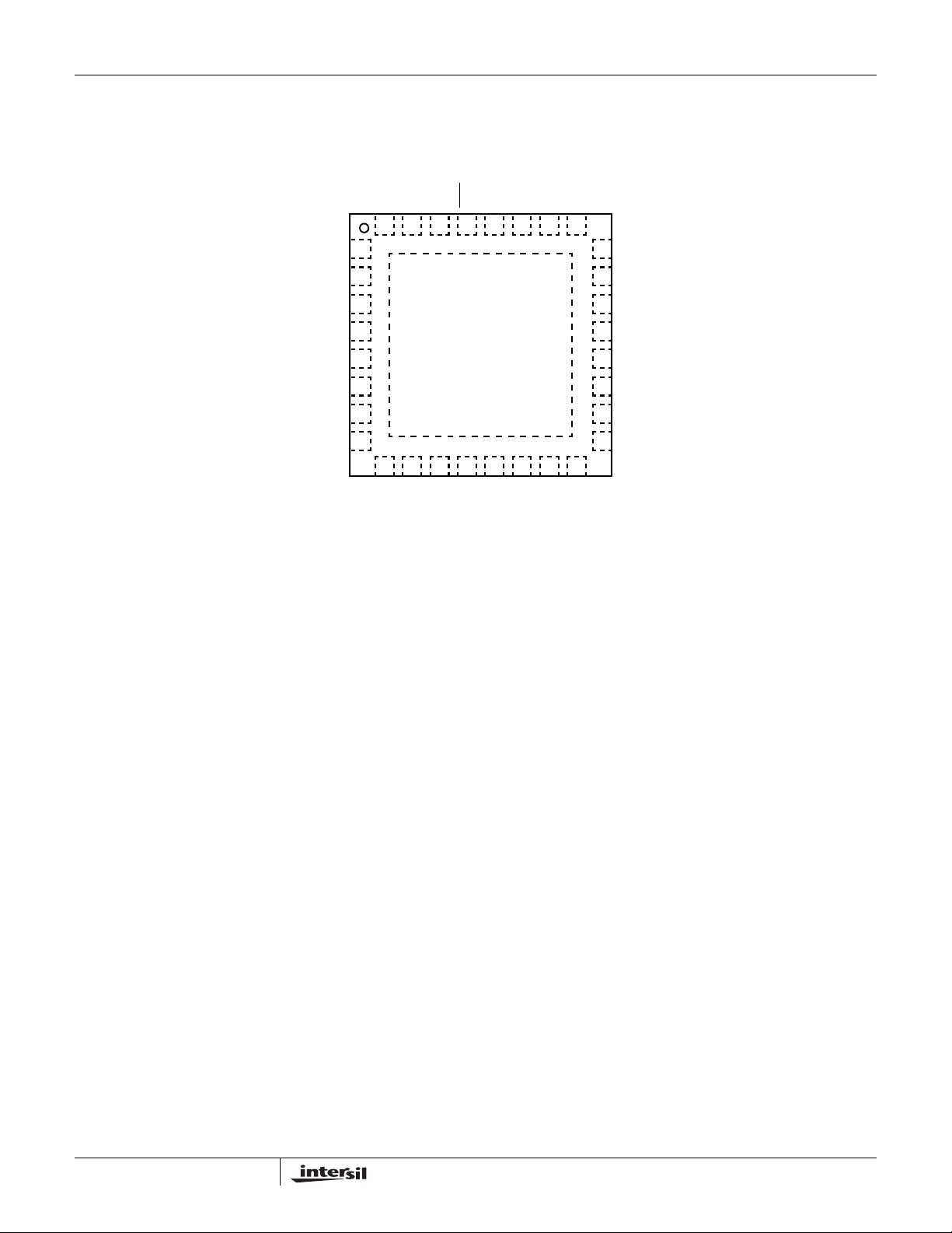
Pinout
REF
ISL6237
ISL6237
(32 LD 5x5 QFN)
TOP VIEW
REFIN2
ILIM2
OUT2
SKIP
POK2
32 31 30 29 28 27 26 25
1
EN2
UGATE2
PHASE2
24
BOOT2
TON
VCC
EN_LDO
NC
VIN
LDO
LDOREFIN
2
3
4
5
6
7
8
9 10111213141516
BYP
FB1
OUT1
ILIM1
POK1
EN1
LGATE2
23
PGND
22
GND
21
NC
20
PVCC
19
LGATE1
18
BOOT1
17
UGATE1
PHASE1
2
FN6418.4
March 18, 2008
ISL6237
Absolute Voltage Ratings
VIN, EN_LDO to GND . . . . . . . . . . . . . . . . . . . . . . . . .-0.3V to +27V
BOOT_ to GND . . . . . . . . . . . . . . . . . . . . . . . . . . . . . .-0.3V to +33V
BOOT_ to PHASE_ . . . . . . . . . . . . . . . . . . . . . . . . . . . .-0.3V to +6V
VCC, EN_, SKIP
PVCC, POK_ to GND . . . . . . . . . . . . . . . . . . . . . . . . . .-0.3V to +6V
LDO, FB1, REFIN2, LDOREFIN to GND . . . -0.3V to (VCC + 0.3V)
OUT_, REF to GND . . . . . . . . . . . . . . . . . . . .-0.3V to (VCC + 0.3V
, TON,
Thermal Information
Thermal Resistance (Typical) θJA (°C/W) θJC (°CW)
32 Ld QFN (Notes 1, 2) . . . . . . . . . . . . 32 3.0
Operating Temperature Range . . . . . . . . . . . . . . . .-40°C to +100°C
Junction Temperature . . . . . . . . . . . . . . . . . . . . . . . . . . . . . .+150°C
Storage Temperature Range . . . . . . . . . . . . . . . . . .-65°C to +150°C
Pb-free reflow profile . . . . . . . . . . . . . . . . . . . . . . . . . .see link below
http://www.intersil.com/pbfree/Pb-FreeReflow.asp
UGATE_ to PHASE_ . . . . . . . . . . . . . . . . . . -0.3V to (PVCC + 0.3V)
ILIM_ to GND. . . . . . . . . . . . . . . . . . . . . . . . . -0.3V to (VCC + 0.3V)
LGATE_, BYP to GND. . . . . . . . . . . . . . . . . -0.3V to (PVCC + 0.3V)
PGND to GND . . . . . . . . . . . . . . . . . . . . . . . . . . . . . .-0.3V to + 0.3V
LDO, REF Short Circuit to GND . . . . . . . . . . . . . . . . . . .Continuous
VCC Short Circuit to GND . . . . . . . . . . . . . . . . . . . . . . . . . . . . . . . 1s
LDO Current (Internal Regulator) Continuous . . . . . . . . . . . . 100mA
LDO Current (Switched Over to OUT1) Continuous . . . . . . +200mA
CAUTION: Do not operate at or near the maximum ratings listed for extended periods of time. Exposure to such conditions may adversely impact product reliability and
result in failures not covered by warranty.
NOTES:
is measured in free air with the component mounted on a high effective thermal conductivity test board with “direct attach” features. See
1. θ
JA
Tech Brief TB379.
2. For θ
, the “case temp” location is the center of the exposed metal pad on the package underside.
JC
3. Limits established by characterization and are not production tested.
4. Parts are 100% tested at +25°C. Temperature limits established by characterization and are not production tested.
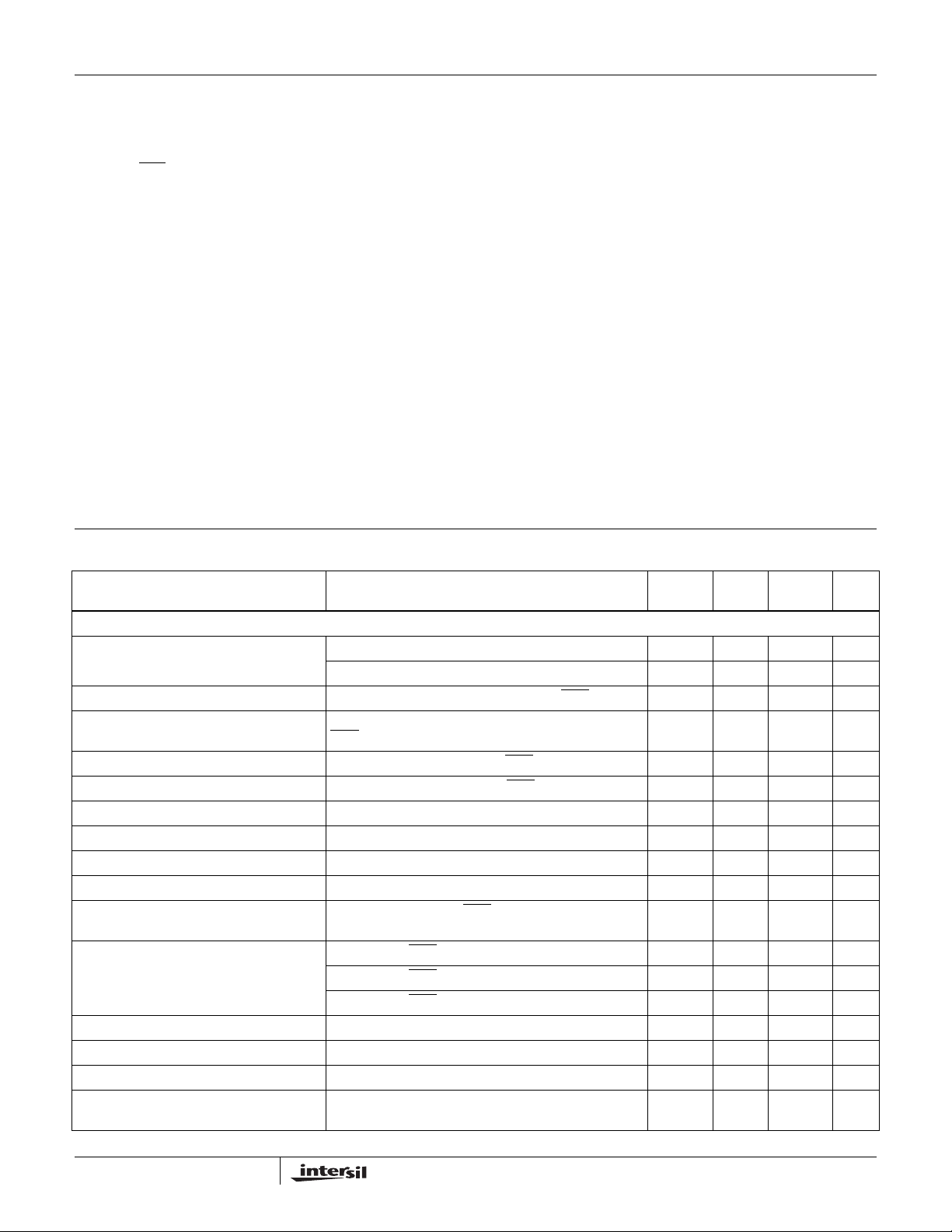
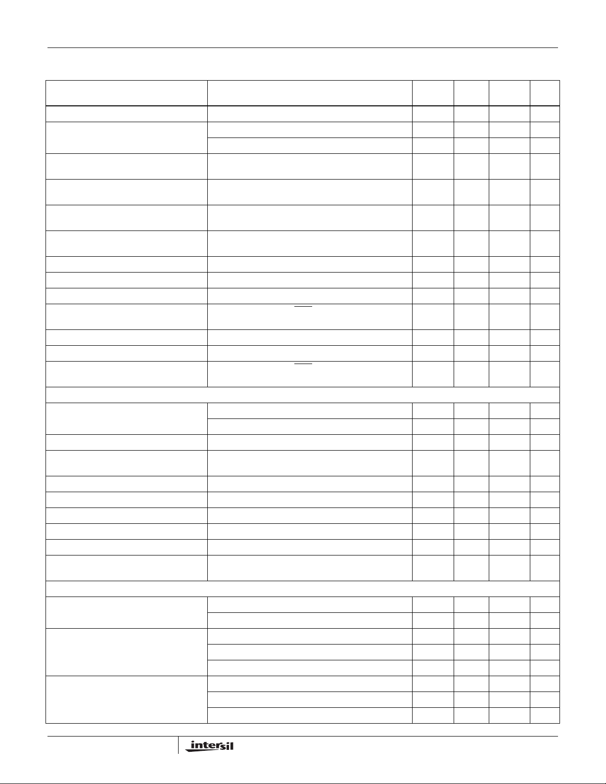
Electrical Specifications No load on LDO, OUT1, OUT2, and REF, V
V
EN_LDO
PARAMETER CONDITIONS
=5V, TA= -40°C to +100°C, unless otherwise noted. Typical values are at TA = +25°C.
= 12V, EN2 = EN1 = VCC, VBYP = 5V, PVCC = 5V,
IN
MIN
(Note 4) TYP
MAX
(Note 4) UNITS
MAIN SMPS CONTROLLERS
VIN Input Voltage Range LDO in regulation 5.5 25 V
= LDO, V
V
IN
< 4.43V 4.5 5.5 V
OUT1
3.3V Output Voltage in Fixed Mode VIN = 5.5V to 25V, REFIN2 > (VCC - 1V), SKIP = 5V 3.285 3.330 3.375 V
1.05V Output Voltage in Fixed Mode V
1.5V Output Voltage in Fixed Mode V
5V Output Voltage in Fixed Mode V
FB1 in Output Adjustable Mode V
= 5.5V to 25V, 3.0 < REFIN2 < (VCC - 1.1V),
IN
SKIP
=5V
= 5.5V to 25V, FB1 = VCC, SKIP = 5V 1.482 1.500 1.518 V
IN
= 5.5V to 25V, FB1 = GND, SKIP = 5V 4.975 5.050 5.125 V
IN
= 5.5V to 25V 0.693 0.700 0.707 V
IN
1.038 1.05 1.062 V
REFIN2 in Output Adjustable Mode VIN = 5.5V to 25V 0.7 2.50 V
SMPS1 Output Voltage Adjust Range SMPS1 0.70 5.50 V
SMPS2 Output Voltage Adjust Range SMPS2 0.50 2.50 V
SMPS2 Output Voltage Accuracy
REFIN2 = 0.7V to 2.5V, SKIP
=VCC -1.0 1.0 %
(Referred for REFIN2)
DC Load Regulation Either SMPS, SKIP
Either SMPS, SKIP
Either SMPS, SKIP
Line Regulation Either SMPS, 6V < V
= VCC, 0 to 5A -0.1 %
= REF, 0 to 5A -1.7 %
= GND, 0 to 5A -1.5 %
< 24V 0.005 %/V
IN
Current-Limit Current Source Temperature = +25°C 4.75 5 5.25 µA
ILIM_ Adjustment Range 0.2 2 V
Current-Limit Threshold (Positive, Default) ILIM_ = VCC, GND - PHASE_
93 100 107 mV
(No temperature compensation)
3
FN6418.4
March 18, 2008
ISL6237
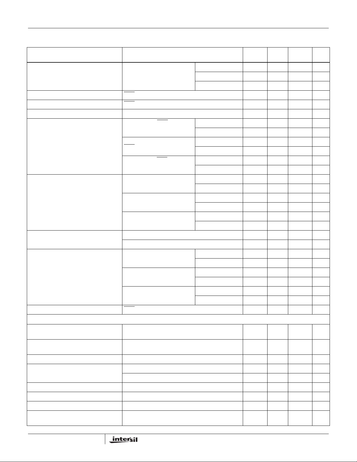
Electrical Specifications No load on LDO, OUT1, OUT2, and REF, V
PARAMETER CONDITIONS
Current-Limit Threshold
(Positive, Adjustable)
V
EN_LDO
=5V, TA= -40°C to +100°C, unless otherwise noted. Typical values are at TA = +25°C. (Continued)
GND - PHASE_ V
= 12V, EN2 = EN1 = VCC, VBYP = 5V, PVCC = 5V,
IN
MIN
(Note 4) TYP
= 0.5V 40 50 60 mV
ILIM_
V
= 1V 93 100 107 mV
ILIM_
V
= 2V 185 200 215 mV
ILIM_
MAX
(Note 4) UNITS
Zero-Current Threshold SKIP = GND, REF, or OPEN, GND - PHASE_ 3 mV
Current-Limit Threshold (Negative, Default) SKIP
= VCC, GND - PHASE_ -120 mV
Soft-Start Ramp Time Zero to full limit 1.7 ms
Operating Frequency (V
= GND), SKIP = VCC SMPS 1 400 kHz
tON
SMPS 2 500 kHz
(V
= REF or OPEN),
tON
SKIP
= VCC
= VCC), SKIP = VCC SMPS 1 200 kHz
(V
tON
SMPS 1 400 kHz
SMPS 2 300 kHz
SMPS 2 300 kHz
On-Time Pulse Width V
Minimum Off-Time T
= GND (400kHz/500kHz) V
tON
V
= REF or OPEN
tON
(400kHz/300kHz)
V
= VCC (200kHz/300kHz) V
tON
= -40°C to +100°C 200 300 425 ns
A
= 5.00V 0.895 1.052 1.209 µs
OUT1
V
= 3.33V 0.475 0.555 0.635 µs
OUT2
V
= 5.05V 0.895 1.052 1.209 µs
OUT1
V
= 3.33V 0.833 0.925 1.017 µs
OUT2
= 5.05V 1.895 2.105 2.315 µs
OUT1
V
= 3.33V 0.833 0.925 1.017 µs
OUT2
TA = -40°C to +85°C 200 300 410 ns
Maximum Duty Cycle V
Ultrasonic SKIP Operating Frequency SKIP
= GND V
tON
V
= REF or OPEN V
tON
V
= VCC V
tON
= 5.05V 88 %
OUT1
V
= 3.33V 85 %
OUT2
= 5.05V 88 %
OUT1
V
= 3.33V 91 %
OUT2
= 5.05V 94 %
OUT1
= 3.33V 91 %
V
OUT2
= REF or OPEN 25 37 kHz
INTERNAL REGULATOR AND REFERENCE
LDO Output Voltage BYP = GND, 5.5V < V
0 < ILDO < 100mA
LDO Output Voltage BYP = GND, 5.5V < V
0 < ILDO < 100mA
LDO Output in Adjustable Mode V
LDO Output Accuracy in Adjustable Mode V
LDOREFIN Input Range V
LDO Output Current BYP = GND, V
LDO Output Current During Switchover BYP = 5V, V
LDO Output Current During Switchover to
3.3V
= 5.5V to 25V, V
IN
= 5.5V to 25V, V
IN
V
= 5.5V to 25V, V
IN
=2xV
LDO
BYP = 3.3V, V
LDOREFIN
= 5.5V to 25V (Note 3) 100 mA
IN
= 5.5V to 25V, LDOREFIN < 0.3V 200 mA
IN
= 5.5V to 25V, LDOREFIN > (VCC - 1V) 100 mA
IN
4
< 25V, LDOREFIN < 0.3V,
IN
< 25V , LDOREFIN> (VCC - 1V),
IN
=2xV
LDO
LDOREFIN
LDOREFIN
LDOREFIN
= 0.35V to 0.5V ±2.5 %
= 0.5V to 2.25V ±1.5 %
4.925 5.000 5.075 V
3.250 3.300 3.350 V
0.7 4.5 V
0.35 2.25 V
FN6418.4
March 18, 2008
ISL6237
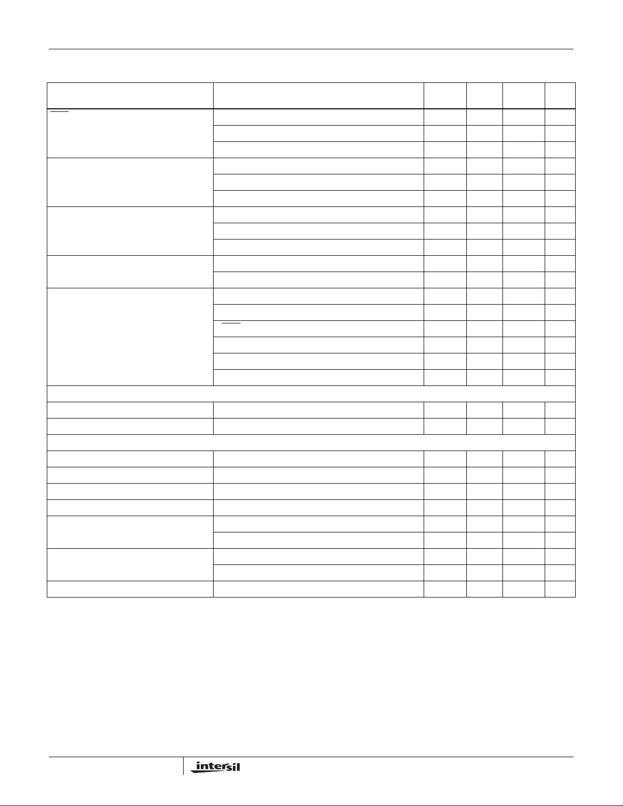
Electrical Specifications No load on LDO, OUT1, OUT2, and REF, V
V
EN_LDO
PARAMETER CONDITIONS
=5V, TA= -40°C to +100°C, unless otherwise noted. Typical values are at TA = +25°C. (Continued)
= 12V, EN2 = EN1 = VCC, VBYP = 5V, PVCC = 5V,
IN
MIN
(Note 4) TYP
MAX
(Note 4) UNITS
LDO Short-Circuit Current LDO = GND, BYP = GND 200 400 mA
Undervoltage-Lockout Fault Threshold Rising edge of PVCC 4.35 4.5 V
Falling edge of PVCC 3.9 4.05 V
LDO 5V Bootstrap Switch Threshold to BYP Rising edge at BYP regulation point
4.53 4.68 4.83 V
LDOREFIN = GND
LDO 3.3V Bootstrap Switch Threshold to
BYP
LDO 5V Bootstrap Switch Equivalent
Rising edge at BYP regulation point
3.0 3.1 3.2 V
LDOREFIN = VCC
LDO to BYP , BYP = 5V, LDOREFIN > (VCC - 1V) (Note 3) 0.7 1.5 Ω
Resistance
LDO 3.3V Bootstrap Switch Equivalent
LDO to BYP, BYP = 3.3V, LDOREFIN < 0.3V (Note 3) 1.5 3.0 Ω
Resistance
REF Output Voltage No external load 1.980 2.000 2.020 V
REF Load Regulation 0 < I
< 50µA 10 mV
LOAD
REF Sink Current REF in regulation 10 µA
VIN Operating Supply Current Both SMPSs on, FB1 = SKIP
V
= BYP = 5.3V, V
OUT1
VIN Standby Supply Current V
VIN Shutdown Supply Current V
= 5.5V to 25V, both SMPSs off, EN_LDO = VCC 180 250 µA
IN
= 4.5V to 25V, EN1 = EN2 = EN_LDO = 0V 20 30 µA
IN
Quiescent Power Consumption Both SMPSs on, FB1 = SKIP
V
= BYP = 5.3V, V
OUT1
= GND, REFIN2 = VCC
= 3.5V
OUT2
= GND, REFIN2 = VCC,
= 3.5V
OUT2
25 50 µA
57mW
FAULT DETECTION
Overvoltage Trip Threshold FB1 with respect to nominal regulation point +8 +11 +14 %
REFIN2 with respect to nominal regulation point +12 +16 +20 %
Overvoltage Fault Propagation Delay FB1 or REFIN2 delay with 50mV overdrive 10 µs
POK_ Threshold FB1 or REFIN2 with respect to nominal output, falling
-12 -9 -6 %
edge, typical hysteresis = 1%
POK_ Propagation Delay Falling edge, 50mV overdrive 10 µs
POK_ Output Low Voltage I
= 4mA 0.2 V
SINK
POK_ Leakage Current High state, forced to 5.5V 1 µA
Thermal-Shutdown Threshold +150 °C
Output Undervoltage Shutdown Threshold FB1 or REFIN2 with respect to nominal output voltage 65 70 75 %
Output Undervoltage Shutdown Blanking
From EN_ signal 10 20 30 ms
Time
INPUTS AND OUTPUTS
FB1 Input Voltage Low level 0.3 V
High level VCC - 1.0 V
REFIN2 Input Voltage OUT2 Dynamic Range, V
OUT2=VREFIN2
0.5 2.50 V
Fixed OUT2 = 1.05V 3.0 VCC - 1.1 V
Fixed OUT2 = 3.3V VCC - 1.0 V
LDOREFIN Input Voltage Fixed LDO = 5V 0.30 V
LDO Dynamic Range, V
LDO
=2xV
LDOREFIN
0.35 2.25 V
Fixed LDO = 3.3V VCC - 1.0 V
5
FN6418.4
March 18, 2008
ISL6237
Electrical Specifications No load on LDO, OUT1, OUT2, and REF, V
V
EN_LDO
PARAMETER CONDITIONS
=5V, TA= -40°C to +100°C, unless otherwise noted. Typical values are at TA = +25°C. (Continued)
= 12V, EN2 = EN1 = VCC, VBYP = 5V, PVCC = 5V,
IN
MIN
(Note 4) TYP
MAX
(Note 4) UNITS
SKIP Input Voltage Low level (SKIP) 0.8 V
Float level (ULTRASONIC SKIP) 1.7 2.3 V
High level (PWM) 2.4 V
TON Input Voltage Low level 0.8 V
Float level 1.7 2.3 V
High level 2.4 V
EN1, EN2 Input Voltage Clear fault level/SMPS off level 0.8 V
Delay start level 1.7 2.3 V
SMPS on level 2.4 V
EN_LDO Input Voltage Rising edge 1.2 1.6 2.0 V
Falling edge 0.94 1.00 1.06 V
Input Leakage Current V
= 0 or 5V -1 +1 µA
tON
V
EN_=VEN_LDO
VSKIP
= 0V or 5V -1 +1 µA
V
= 0V or 5V -0.2 +0.2 µA
FB1
V
= 0V or 2.5V -0.2 +0.2 µA
REFIN
V
LDOREFIN
= 0V or 5V -0.1 +0.1 µA
= 0V or 2.75V -0.2 +0.2 µA
INTERNAL BOOT DIODE
V
Forward Voltage PVCC - V
D
I
BOOT_LEAKAGE
Leakage Current V
BOOT
, IF= 10mA 0.65 0.8 V
BOOT
= 30V, PHASE = 25V, PVCC = 5V 500 nA
MOSFET DRIVERS
UGATE_ Gate-Driver Sink/Source Current UGATE1, UGATE2 forced to 2V 2 A
LGATE_ Gate-Driver Source Current LGATE1 (source), LGATE2 (source), forced to 2V 1.7 A
LGATE_ Gate-Driver Sink Current LGATE1 (sink), LGATE2 (sink), forced to 2V 3.3 A
UGATE_ Gate-Driver ON-resistance BST_ - PHASE_ forced to 5V (Note 3) 1.5 4.0 Ω
LGATE_ Gate-Driver ON-resistance LGATE_, high state (pull-up) (Note 3) 2.2 5.0 Ω
LGATE_, low state (pull-down) (Note 3) 0.6 1.5 Ω
Dead Time LGATE_ Rising 15 20 35 ns
UGATE_ Rising 20 30 50 ns
OUT1, OUT2 Discharge ON-resistance 25 40 Ω
6
FN6418.4
March 18, 2008
ISL6237
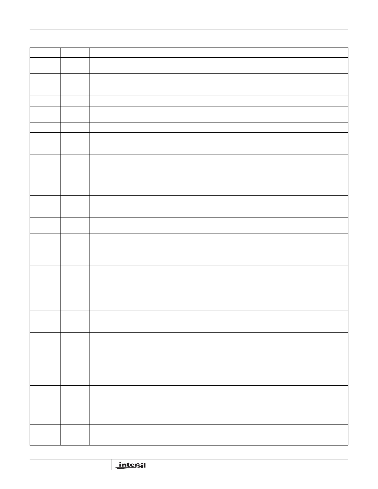
Pin Descriptions
PIN NAME FUNCTION
1
2
3
4
5
6
7
8
9
10
11
12
13
14
15
16
17
18
19
20
21
22
REF 2V Reference Output. Bypass to GND with a 0.1µF (min) capacitor. REF can source up to 50µA for external loads.
Loading REF degrades FB and output accuracy according to the REF load-regulation error.
TON Frequency Select Input. Connect to GND for 400kHz/500kHz operation. Connect to REF (or leave OPEN) for
400kHz/300kHz operation. Connect to VCC for 200kHz/300kHz operation (5V/3.3V SMPS switching frequencies,
respectively.)
VCC Analog Supply Voltage Input for PWM Core. Bypass to GND with a 1µF ceramic capacitor.
EN_LDO LDO Enable Input. The LDO is enabled if EN_LDO is within logic high level and disabled if EN_LDO is less than the
logic low level.
NC No connect.
VIN Power-Supply Input. VIN is used for the constant-on-time PWM on-time one-shot circuits. VIN is also used to power
the linear regulators. The linear regulators are powered by SMPS1 if OUT1 is set greater than 4.78V and BYP is tied
to OUT1. Connect VIN to the battery input and bypass with a 1µF capacitor.
LDO Linear-Regulator Output. LDO can provide a total of 100mA external loads. The LDO regulate at 5V If LDOREFIN is
connected to GND. When the LDO is set at 5V and BYP is within 5V switchover threshold, the internal regulator shuts
down and the LDO output pin connects to BYP through a 0.7Ω switch. The LDO regulate at 3.3V if LDOREFIN is
connected to VCC. When the LDO is set at 3.3V and BYP is within 3.3V switchover threshold, the internal regulator
shuts down and the LDO output pin connects to BYP through a 1.5Ω switch. Bypass LDO output with a minimum of
4.7µF ceramic.
LDOREFIN LDO Reference Input. Connect LDOREFIN to GND for fixed 5V operation. Connect LDOREFIN to VCC for fixed 3.3V
operation. LDOREFIN can be used to program LDO output voltage from 0.7V to 4.5V. LDO output is two times the
voltage of LDOREFIN. There is no switchover in adjustable mode.
BYP BYP is the switchover source voltage for the LDO when LDOREFIN connected to GND or VCC. Connect BYP to 5V if
LDOREFIN is tied GND. Connect BYP to 3.3V if LDOREFIN is tied to VCC.
OUT1 SMPS1 Output Voltage-Sense Input. Connect to the SMPS1 output. OUT1 is an input to the Constant on-time-PWM
on-time one-shot circuit. It also serves as the SMPS1 feedback input in fixed-voltage mode.
FB1 SMPS1 Feedback Input. Connect FB1 to GND for fixed 5V operation. Connect FB1 to VCC for fixed 1.5V operation
Connect FB1 to a resistive voltage-divider from OUT1 to GND to adjust the output from 0.7V to 5.5V.
ILIM1 SMPS1 Current-Limit Adjustment. The GND-PHASE1 current-limit threshold is 1/10th the voltage seen at ILIM1 over
a 0.2V to 2V range. There is an internal 5µA current source from VCC to ILIM1. Connect ILIM1 to REF for a fixed
200mV threshold. The logic current limit threshold is default to 100mV value if ILIM1 is higher than VCC - 1V.
POK1 SMPS1 Power-Good Open-Drain Output. POK1 is low when the SMPS1 output voltage is more than 10% below the
normal regulation point or during soft-start. POK1 is high impedance when the output is in regulation and the soft-start
circuit has terminated. POK1 is low in shutdown.
EN1 SMPS1 Enable Input. The SMPS1 is enabled if EN1 is greater than the logic high level and disabled if EN1 is less than
the logic low level. If EN1 is connected to REF, the SMPS1 starts after the SMPS2 reaches regulation (delay start).
Drive EN1 below 0.8V to clear fault level and reset the fault latches.
UGATE1 High-Side MOSFET Floating Gate-Driver Output for SMPS1. UGATE1 swings between PHASE1 and BOOT1.
PHASE1 Inductor Connection for SMPS1. PHASE1 is the internal lower supply rail for the UGATE1 high-side gate driver.
PHASE1 is the current-sense input for the SMPS1.
BOOT1 Boost Flying Capacitor Connection for SMPS1. Connect to an external capacitor according to the “Typical Application
Circuits” starting on page 21 (Figures 62, 63 and 64). See “MOSFET Gate Drivers (UGATE_, LGATE_)” on page 28.
LGATE1 SMPS1 Synchronous-Rectifier Gate-Drive Output. LGATE1 swings between GND and PVCC.
PVCC PVCC is the supply voltage for the low-side MOSFET driver LGATE. Connect a 5V power source to the PVCC pin and
bypass to PGND with a 1µF MLCC ceramic capacitor. Refer to Figure 65 - A switch connects PVCC to VCC with 10
when in normal operation and is disconnected when in shutdown mode. An external 10Ω resistor from PVCC to VCC
is prohibited as it will create a leakage path from VIN to GND in shutdown mode.
NC No connect.
GND Analog Ground for both SMPS_ and LDO. Connect externally to the underside of the exposed pad.
PGND Power Ground for SMPS_ controller. Connect PGND externally to the underside of the exposed pad.
Ω
7
FN6418.4
March 18, 2008
ISL6237
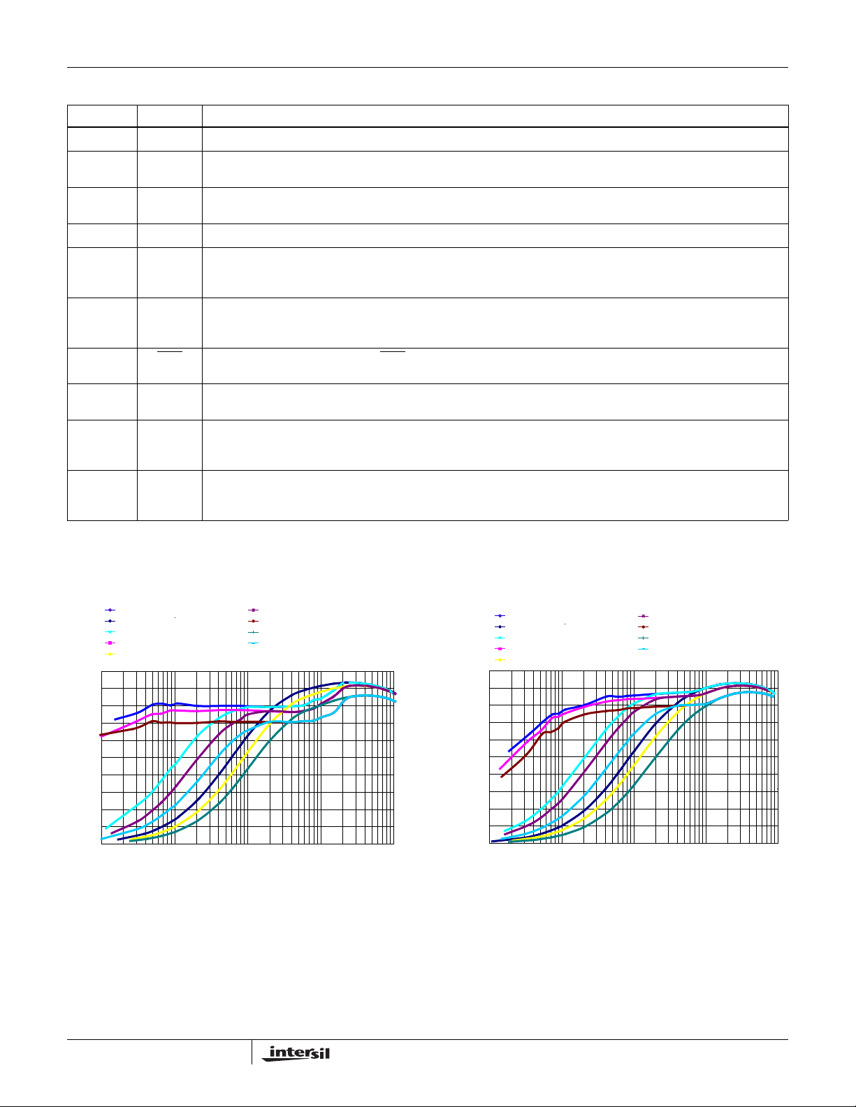
Pin Descriptions (Continued)
PIN NAME FUNCTION
23
24
25
26
27
28
29
30
31
32
LGATE2 SMPS2 Synchronous-Rectifier Gate-Drive Output. LGATE2 swings between GND and PVCC.
BOOT2 Boost Flying Capacitor Connection for SMPS2. Connect to an external capacitor according to the “Typical Application
Circuits” starting on page 21 (Figures 62, 63 and 64) See “MOSFET Gate Drivers (UGATE_, LGATE_)” on page 28.
PHASE2 Inductor Connection for SMPS2. PHASE2 is the internal lower supply rail for the UGATE2 high-side gate driver.
PHASE2 is the current-sense input for the SMPS2.
UGATE2 High-Side MOSFET Floating Gate-Driver Output for SMPS2. UGATE1 swings between PHASE2 and BOOT2.
EN2 SMPS2 Enable Input. The SMPS2 is enabled if EN2 is greater than the logic high level and disabled if EN2 is less than
the logic low level. If EN2 is connected to REF, the SMPS2 starts after the SMPS1 reaches regulation (delay start).
Drive EN2 below 0.8V to clear fault level and reset the fault latches.
POK2 SMP2 Power-Good Open-Drain Output. POK2 is low when the SMPS2 output voltage is more than 10% below the
normal regulation point or during soft-start. POK2 is high impedance when the output is in regulation and the soft-start
circuit has terminated. POK2 is low in shutdown.
SKIP
Low-Noise Mode Control. Connect SKIP to GND for normal Idle-Mode (pulse-skipping) operation or to VCC for PWM
mode (fixed frequency). Connect to REF or leave floating for ultrasonic skip mode operation.
OUT2 SMPS2 Output Voltage-Sense Input. Connect to the SMPS2 output. OUT2 is an input to the Constant on-time-PWM
on-time one-shot circuit. It also serves as the SMPS2 feedback input in fixed-voltage mode.
ILIM2 SMPS2 Current-Limit Adjustment. The GND-PHASE1 current-limit threshold is 1/10th the voltage seen at ILIM2 over
a 0.2V to 2V range. There is an internal 5µA current source from VCC to ILIM2. Connect ILIM2 to REF for a fixed
200mV. The logic current limit threshold is default to 100mV value if ILIM2 is higher than VCC - 1V.
REFIN2 Output volt age control for SMPS2. Connect REFIN2 to VCC for fixed 3.3V. Connect REFIN2 to a 3.3V supply for fixed
1.05V. REFIN2 can be used to program SMPS2 output voltage from 0.5V to 2.50V. SMPS2 output voltage is 0V if
REFIN2 < 0.5V.
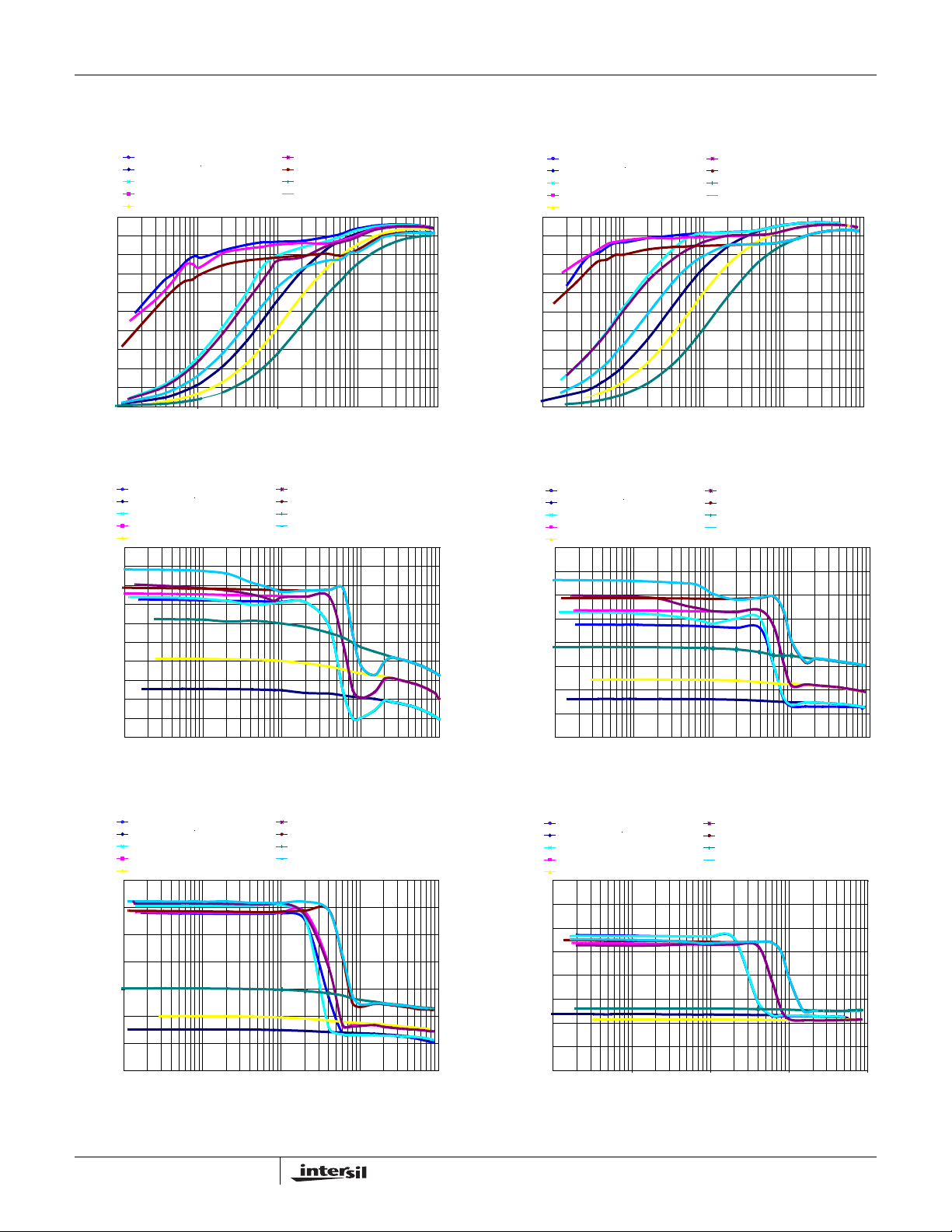
Typical Performance Curves Circuit of Figures 62, 63 and 64, no load on LDO, OUT1, OUT2, and REF, V
7 VIN SKIP MODE
7 VIN PWM MODE
7 VIN ULTRA SKIP MODE
12 VIN SKIP MODE
12 V
PWM MODE
100
90
80
70
60
50
40
EFFICIENCY (%)
30
20
10
0
0.001 0.010 0.100
FIGURE 1. V
IN
OUTPUT LOAD (A)
= 1.05V EFFICIENCY vs LOAD (300kHz) FIGURE 2. V
OUT2
EN2 = EN1 = VCC, VBYP = 5V, PVCC = 5V, V
otherwise noted. Typical values are at T
12 V
ULTRA SKIP MODE
IN
25 VIN SKIP MODE
25 VIN PWM MODE
ULTRA SKIP MODE
25 V
IN
1.000
10.000
EN_LDO
= +25°C.
A
7 VIN SKIP MODE
7 VIN PWM MODE
7 VIN ULTRA SKIP MODE
12 VIN SKIP MODE
PWM MODE
12 V
100
90
80
70
60
50
40
30
EFFICIENCY (%)
20
10
0
0.001
IN
OUT1
=5V, TA= -40°C to +100°C, unless
12 V
IN
25 VIN SKIP MODE
25 VIN PWM MODE
25 V
IN
0.010 0.100 1.000 10.000
OUTPUT LOAD (A)
= 1.5V EFFICIENCY vs LOAD (200kHz)
=12V,
IN
ULTRA SKIP MODE
ULTRA SKIP MODE
8
FN6418.4
March 18, 2008
ISL6237
Typical Performance Curves Circuit of Figures 62, 63 and 64, no load on LDO, OUT1, OUT2, and REF, V
EN2 = EN1 = VCC, VBYP = 5V, PVCC = 5V, V
otherwise noted. Typical values are at T
7 VIN SKIP MODE
7 VIN PWM MODE
7 VIN ULTRA SKIP MODE
12 VIN SKIP MODE
PWM MODE
12 V
100
90
80
70
60
50
40
30
EFFICIENCY (%)
20
10
0
0.001 0.010 0.100 1.000 10.000
FIGURE 3. V
1.070
1.068
1.066
1.064
1.062
1.060
1.058
1.056
OUTPUT VOLTAGE (V)
1.054
1.052
1.050
FIGURE 5. V
IN
OUTPUT LOAD (A)
= 3.3V EFFICIENCY vs LOAD (500kHz) FIGURE 4.
OUT2
7 VIN SKIP MODE
7 VIN PWM MODE
7 VIN ULTRA SKIP MODE
12 VIN SKIP MODE
12 V
PWM MODE
IN
0.001 0.010 0.100 1.000 10.000
OUTPUT LOAD (A)
= 1.05V REGULATION vs LOAD (300kHz) FIGURE 6. V
OUT2
12 V
ULTRA SKIP MODE
IN
25 VIN SKIP MODE
25 VIN PWM MODE
25 V
ULTRA SKIP MODE
IN
12 V
ULTRA SKIP MODE
IN
25 VIN SKIP MODE
25 VIN PWM MODE
ULTRA SKIP MODE
25 V
IN
EN_LDO
= +25°C. (Continued)
A
7 VIN SKIP MODE
7 VIN PWM MODE
7 VIN ULTRA SKIP MODE
12 VIN SKIP MODE
12 V
PWM MODE
100
90
80
70
60
50
EFFICIENCY (%)
40
30
20
10
0
0.001 0.010 0.100 1.000 10.000
IN
VOUT1
7 VIN SKIP MODE
7 VIN PWM MODE
7 VIN ULT RA SKIP MODE
12 VIN SKIP MODE
12 V
PWM MODE
IN
0.001 0.010 0.100 1.000
OUTPUT VOLTAGE (V)
1.540
1.535
1.530
1.525
1.520
1.515
1.510
1.505
1.500
OUT1
=5V, TA= -40°C to +100°C, unless
12 V
IN
25 VIN SKIP MODE
25 VIN PWM MODE
25 V
IN
OUTPUT LOAD (A)
= 5V EFFICIENCY vs LOAD (400kHz)
12 V
IN
25 VIN SKIP MODE
25 VIN PWM MODE
25 V
IN
OUTPUT LOAD (A)
= 1.5V REGULATION vs LOAD (200kHz)
=12V,
IN
ULTRA SKIP MODE
ULTRA SKIP MODE
ULTRA SKIP MODE
ULTRA SKIP MODE
10.000
7 VIN SKIP MODE
7 VIN PWM MODE
7 VIN ULTRA SKIP MODE
12 VIN SKIP MODE
12 V
PWM MODE
3.38
3.37
3.36
3.35
3.34
3.33
OUTPUT VOLTAGE (V)
3.32
3.31
FIGURE 7. V
IN
0.001 0.010 0.100 1.000 10.000
OUT2
OUTPUT LOAD (A)
= 3.3V REGULATION vs LOAD (500kHz) FIGURE 8. V
12 V
ULTRA SKIP MODE
IN
25 VIN SKIP MODE
25 VIN PWM MODE
ULTRA SKIP MODE
25 V
IN
9
7 VIN SKIP MODE
7 VIN PWM MODE
7 VIN ULTRA SKIP MODE
12 VIN SKIP MODE
PWM MODE
12 V
5.16
5.14
5.12
5.10
5.08
5.06
5.04
OUTPUT VOLTAGE (V)
5.02
5.00
IN
0.001 0.010 0.100 1.000 10.000
OUT1
OUTPUT LOAD (A)
= 5V REGULATION vs LOAD (400kHz)
12 V
ULTRA SKIP MODE
IN
25 VIN SKIP MODE
25 VIN PWM MODE
ULTRA SKIP MODE
25 V
IN
FN6418.4
March 18, 2008
ISL6237
Typical Performance Curves Circuit of Figures 62, 63 and 64, no load on LDO, OUT1, OUT2, and REF, V
EN2 = EN1 = VCC, VBYP = 5V, PVCC = 5V, V
otherwise noted. Typical values are at T
7 VIN SKIP MODE
7 VIN PWM MODE
7 VIN ULTRA SKIP MODE
12 VIN SKIP MODE
PWM MODE
12 V
2.5
2.0
1.5
1.0
0.5
POWER DISSIPATION (W)
0
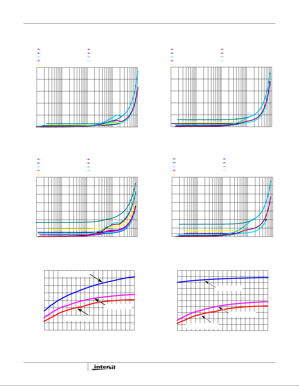
0.001 0.010 0.100 1.000 10.000
FIGURE 9. V
3.5
IN
OUTPUT LOAD (A)
= 1.05V POWER DISSIPATION vs LOAD
OUT2
(300kHz)
7 VIN SKIP MODE
7 VIN PWM MODE
7 VIN ULTRA SKIP MODE
12 VIN SKIP MODE
PWM MODE
12 V
IN
12 V
ULTRA SKIP MODE
IN
25 VIN SKIP MODE
25 VIN PWM MODE
25 V
ULTRA SKIP MODE
IN
12 V
ULTRA SKIP MODE
IN
25 VIN SKIP MODE
25 VIN PWM MODE
25 V
ULTRA SKIP MODE
IN
EN_LDO
= +25°C. (Continued)
A
7 VIN SKIP MODE
7 VIN PWM MODE
7 VIN ULTRA SKIP MODE
12 VIN SKIP MODE
PWM MODE
12 V
2.5
2.0
1.5
1.0
0.5
POWER DISSIPATION (W)
FIGURE 10. V
3.5
IN
0
0.001 0.010 0.100 1.000 10.000
OUT1
(200kHz)
7 VIN SKIP MODE
7 VIN PWM MODE
7 VIN ULTRA SKIP MODE
12 VIN SKIP MODE
PWM MODE
12 V
IN
=5V, TA= -40°C to +100°C, unless
12 V
IN
25 VIN SKIP MODE
25 VIN PWM MODE
25 V
IN
OUTPUT LOAD (A)
= 1.5V POWER DISSIPA TION vs LOAD
12 V
IN
25 VIN SKIP MODE
25 VIN PWM MODE
25 V
IN
=12V,
IN
ULTRA SKIP MODE
ULTRA SKIP MODE
ULTRA SKIP MODE
ULTRA SKIP MODE
3.0
2.5
2.0
1.5
1.0
POWER DISSIPATION (W)
0.5
0
0.001 0.010 0.100 1.000 10.000
FIGURE 11. V
1.064
1.062
1.060
1.058
1.056
1.054
1.052
OUTPUT VOLTAGE (V)
1.050
1.048
FIGURE 13. V
OUT2
(500kHz)
5791113151719212325
OUT2
vs V
OUTPUT LOAD (A)
= 3.3V POWER DISSIPATION vs LOAD
NO LOAD PWM
MID LOAD PWM
MAX LOAD PWM
INPUT VOLTAGE (V)
= 1.05V OUTPUT VOLTAGE REGULATION
(PWM MODE)
IN
3.0
2.5
2.0
1.5
1.0
POWER DISSIPATION (W)
0.5
0
0.001 0.010 0.100 1.000 10.000
FIGURE 12. V
1.068
1.066
1.064
1.062
1.060
1.058
1.056
1.054
OUTPUT VOLTAGE (V)
1.052
1.050
1.048
FIGURE 14. V
OUT1
(400kHz)
MAX LOAD PWM
MAX LOAD PWM
5791113151719212325
OUT2
vs V
IN
OUTPUT LOAD (A)
= 5V POWER DISSIPA TION vs LOAD
NO LOAD PWM
MID LOAD PWM
INPUT VOLTAGE (V)
= 1.05V OUTPUT VOLT AGE REGULA TION
(SKIP MODE)
10
FN6418.4
March 18, 2008
ISL6237
Typical Performance Curves Circuit of Figures 62, 63 and 64, no load on LDO, OUT1, OUT2, and REF, V
1.518
1.516
1.514
1.512
1.510
1.508
OUTPUT VOLTAGE (V)
1.506
1.504
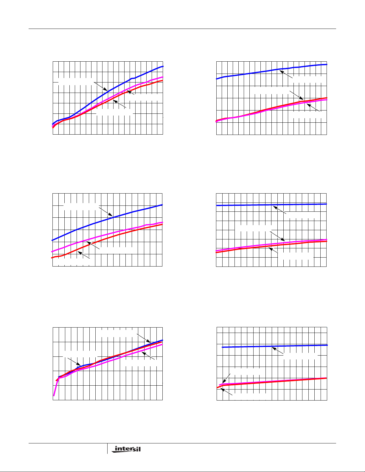
5791113151719212325
FIGURE 15. V
3.340
3.335
3.330
3.325
3.320
OUTPUT VOLTAGE (V)
3.315
3.310
MAX LOAD PWM
7 9 11 13 15 17 19 21 23 25
FIGURE 17. V
EN2 = EN1 = VCC, VBYP = 5V, PVCC = 5V, V
otherwise noted. Typical values are at T
NO LOAD PWM
MID LOAD PWM
MAX LOAD PWM
INPUT VOLTAGE (V)
= 1.5V OUTPUT VOLTAGE REGULA TION
OUT1
vs V
(PWM MODE)
IN
NO LOAD PWM
MID LOAD PWM
INPUT VOLTAGE (V)
= 3.3V OUTPUT VOLTAGE REGULA TION
OUT2
vs V
(PWM MODE)
IN
= +25°C. (Continued)
A
1.530
1.525
1.520
1.515
1.510
OUTPUT VOLTAGE (V)
1.505
1.500
5791113151719212325
FIGURE 16. V
3.38
3.37
3.36
3.35
3.34
3.33
3.32
OUTPUT VOLTAGE (V)
3.31
3.30
7 9 11 13 15 17 19 21 23 25
FIGURE 18. V
EN_LDO
OUT1
vs V
OUT2
vs V
=5V, TA= -40°C to +100°C, unless
MID LOAD PWM
INPUT VOLTAGE (V)
= 1.5V OUTPUT VOLT AGE REGULA TION
(SKIP MODE)
IN
NO LOAD PWM
MAX LOAD PWM
MID LOAD PWM
INPUT VOLTAGE (V)
= 3.3V OUTPUT VOLTAGE REGULA TION
(SKIP MODE)
IN
=12V,
IN
NO LOAD PWM
MAX LOAD PWM
5.065
5.060
5.055
5.050
OUTPUT VOLTAGE (V)
5.045
5.040
7 9 11 13 15 17 19 21 23 25
FIGURE 19. V
NO LOAD PWM
MAX LOAD PWM
MID LOAD PWM
INPUT VOLTAGE (V)
= 5V OUTPUT VOLT AGE REGULA TION vs
OUT1
V
(PWM MODE)
IN
11
5.14
5.12
5.10
5.08
5.06
OUTPUT VOLTAGE (V)
5.04
5.02
7 9 11 13 15 17 19 21 23 25
FIGURE 20. V
NO LOAD PWM
MID LOAD PWM
MAX LOAD PWM
INPUT VOLTAGE (V)
= 5V OUTPUT VOLT AGE REGULA TION vs
OUT1
V
(SKIP MODE)
IN
FN6418.4
March 18, 2008
 Loading...