

®
ISL6227
December 21, 2006Data Sheet FN9094.4
Dual Mobile-Friendly PWM Controller with
DDR Option
The ISL6227 dual PWM controller delivers high efficiency
precision voltage regulation from two synchronous buck DC/DC
converters. It was designed especially to provide power
regulation for DDR memory, chip sets, graphics and other
system electronics in Notebook PCs. The ISL6227’s wide
input voltage range capability allows for voltage conversion
directly from AC/DC adaptor or Li-Ion battery pack.
Automatic mode transition of constant-frequency synchronous
rectification at heavy load, and hysteretic (HYS) diodeemulation at light load, assure high efficiency over a wide range
of conditions. The HYS mode of operation can be disabled
separately on each PWM converter if constant-frequency
continuous-conduction operation is desired for all load levels.
Efficiency is further enhanced by using the lower MOSFET
r
Voltage-fe ed-forward ramp modulation, current mode control,
and internal feedback compensation provide fast response to
input voltage and load transients. Input current ripple is
minimized by channel-to-channel PWM phase shift of 0°, 90° or
180° (determined by input voltage and status of the DDR pin).
The ISL6227 can control two inde pendent ou tput volt ages
adjustable from 0.9V to 5.5V, or by activating the DDR pin,
transform into a complete DDR memory power supply solution.
In DDR mode, CH2 output voltage VTT tracks CH1 output
voltage VDDQ. CH2 output can bo th source and sink current, an
essential power supply feature for DDR memory. The reference
voltage VREF required by DDR memory is generated as well.
In dual power supply applications the ISL6227 monitors the
output voltage of both CH1 and CH2. An independent PGOOD
(power good) signal is asserted for each channel after the
soft-start sequence has completed, and the output voltage is
within PGOOD window. In DDR mode CH1 generates the only
PGOOD signal.
Built-in overvoltage protection prevents the output from going
above 115% of the set point by holding the lower MOSFET on
and the upper MOSFET off. When the output voltage re-enters
regulation, PGOOD will go HIGH and normal operation
automatically resumes. Once the soft-start sequence has
completed, undervoltage protection latches the offending
channel off if the output drops below 75% of its set point value.
Adjustable overcurrent protection (OCP) monitors the voltage
drop across the r
current-sensing is required, an external current sense resistor
may be used.
as the current sense element.
DS(ON)
DS(ON)
of the lower MOSFET. If more precise
Features
• Provides regulated output voltage in the range 0.9V–5.5V
• Operates from an input battery voltage range of 5V to 24V
or from 3.3V/5V system rail
• Complete DDR1 and DDR2 memory power solution with
VTT tracking VDDQ/2 and a VDDQ/2 buffered reference
output
• Flexible PWM or HYS plus PWM mode selection with HYS
diode emulation at light loads for higher system efficiency
•r
current sensing
DS(ON)
• Excellent dynamic response with voltage feed-forward and
current mode control accommodating wide range LC filter
selections
• Undervoltage lock-out on VCC pin
• Power-good, overcurrent, overvoltage, undervoltage
protection for both channels
• Synchronized 300kHz PWM operation in PWM mode
• Pb-free plus anneal available (RoHS compliant)
Applications
• Notebook PCs and Desknotes
• Tablet PCs/Slates
• Hand-held portable instruments
Ordering Information
PART
PART #
ISL6227CA ISL6227CA -10 to +100 28 Ld QSOP M28.15
ISL6227CAZ
(Note)
ISL6227IA ISL6227IA -40 to +100 28 Ld QSOP M28.15
ISL6227IAZ
(Note)
ISL6227HRZ
(Note)
ISL6227IRZ
(Note)
Add -T to part number for Tape and Reel
NOTE: Intersil Pb-free plus anneal product s empl oy special Pb -free
material sets; molding compounds/die attach materials and 100% matte
tin plate termination finish, which are RoH S compliant and comp atible
with both SnPb and Pb-free soldering operations. Intersil Pb-free
products are MSL classifie d at Pb-fre e peak ref low te mperat ures tha t
meet or exceed the Pb-free requirements of IPC/JEDEC J STD-020.
MARKING
ISL6227CAZ -10 to +100 28 Ld QSOP
ISL6227IAZ -40 to +100 28 Ld QSOP
ISL6227HRZ -10 to +100 28 Ld QFN
ISL6227IRZ -40 to +100 28 Ld QFN
TEMP.
RANGE (°C)
PACKAGE
(Pb-free)
(Pb-free)
(Pb-free)
(Pb-free)
PKG.
DWG. #
M28.15
M28.15
L28.5x5
L28.5x5
1
CAUTION: These devices are sensitive to electrostatic discharge; follow proper IC Handling Procedures.
1-888-INTERSIL or 1-888-468-3774
| Intersil (and design) is a registered trademark of Intersil Americas Inc.
All other trademarks mentioned are the property of their respective owners.
Copyright Intersil Americas Inc. 2004-2006. All Rights Reserved
Pinouts
28LD SSOP
TOP VIEW
ISL6227
28 LD 5X5 QFN
TOP VIEW
1
GND
LGATE1
PHASE1
UGATE1
2
3
PGND1
4
5
6
BOOT1
7
ISEN1
8
EN1
9
VOUT1
10
VSEN1
11
SOFT1 SOFT2
12
DDR
13
VIN PG1
14
28
27
26
25
24
23
22
21
20
19
18
17
16
15
Generic Application Circuits
V
IN
+5V to +24V
+5V
VCC
LGATE2
PGND2
PHASE2
UGATE2
BOOT2
ISEN2
EN2
VOUT2
VSEN2
OCSET2OCSET1
PG2/REF
OCSET1
OCSET2
EN1
EN2
VCC
DDR
PWM1
PWM2
Q1
Q2
PHASE1
UGATE1
BOOT1
ISEN1
EN1
VOUT1
VSEN1
PGN1
LGATE1
28 27 26 25 24 23 22
1
2
3
4
5
6
7
8 9 10 11 12 13 14
SOFT1
OCSET1
L1
+
C1
Q3
Q4
GND
GND
29
DDR
VCC
LGATE2
PGND2
PHASE2
21
UGATE2
20
BOOT2
19
ISEN2
18
EN2
17
VOUT2
16
VSEN2
15
OCSET2
VIN
PG1
SOFT2
PG2/REF
V
OUT1
+1.80V
L2
C2
V
OUT2
+1.20V
+
V
IN
+5V to 24V
VREF
+1.25V
ISL6227 APPLICATION CIRCUIT FOR TWO CHANNEL POWER SUPPLY
+5V
OCSET1
EN1
EN2
VCC
DDR
PG2/VREF
PWM1
PWM2
Q1
Q2
OCSET2
L1
C1
+
Q3
Q4
ISL6227 APPLICATION CIRCUIT FOR COMPLETE DDR MEMORY POWER SUPPLY
2
L2
C2
VDDQ
+2.50V
VTT
+1.25V
+
FN9094.4
December 21, 2006
ISL6227
Absolute Maximum Ratings
Bias Voltage, VCC. . . . . . . . . . . . . . . . . . . . . . . GND - 0.3V to +6.5V
Input Voltage, V
PHASE, UGATE . . . . . . . . . . . . . . . . . . . .GND-5V (Note 1) to 33.0V
BOOT, ISEN . . . . . . . . . . . . . . . . . . . . . . . . . . . GND-0.3V to +33.0V
BOOT with Respect to PHASE . . . . . . . . . . . . . . . . . . . . . . . . + 6.5V
All Other Pins. . . . . . . . . . . . . . . . . . . . . . GND -0.3V to V
. . . . . . . . . . . . . . . . . . . . . . GND - 0.3V to +25.0V
IN
+ 0.3V
CC
Thermal Information
Thermal Resistance (Typical) θJA (°C/W) θJC (°C/W)
SSOP Package (Note 2)
QFN Package(Notes 3, 4)
Maximum Junction Temperature (Plastic Package). . . . . . . . +150°C
. . . . . . . . . . . . . .
. . . . . . . . . . . .
Maximum Storage Temperature Range. . . . . . . . . .-65°C to +150°C
80 N/A
36 6
Recommended Operating Conditions
Bias Voltage, VCC . . . . . . . . . . . . . . . . . . . . . . . . . . . . . +5.0V ± 5%
Input Voltage, V
. . . . . . . . . . . . . . . . . . . . . . . . . . .+5.0V to +24.0V
IN
Ambient Temperature Range . . . . . . . . . . . . . . . . . -10°C to +100°C
Junction Temperature Range. . . . . . . . . . . . . . . . . -10°C to +125°C
CAUTION: Stresses above those listed in “Absolute Maximum Ratings” may cause permanent damage to the device. This is a stress only rating and operation of the
device at these or any other conditions above those indicated in the operational sections of this specification is not implied.
NOTES:
1. 250ns transient. See Confining The Negative Phase Node Voltage Swing in Application Information Section
is measured with the component mounted on a high effective thermal conductivity test board in free air. See Tech Brief TB379 for details.
2. θ
JA
is measured in free air with the component mounted on a high effective thermal conductivity test board with “direct attach” features. See T ech
3. θ
JA
Brief TB379.
4. For θ
, the “case temp” location is the center of the exposed metal pad on the package underside.
JC
Electrical Specifications Recommended Operating Conditions, Unless Otherwise Noted.
PARAMETER SYMBOL TEST CONDITIONS MIN TYP MAX UNITS
VCC SUPPLY
Bias Current I
Shut-down Current I
CC
CCSN
LGATEx, UGATEx Open, VSENx forced above
regulation point, V
IN
> 5V
VCC UVLO
Rising VCC Threshold V
Falling VCC Threshold V
V
IN
Input Voltage Pin Current (Sink) I
Shut-Down Current I
CCU
CCD
VIN
VINS
OSCILLATOR
PWM1 Oscillator Frequency F
Commercial, ISL6227C 255 300 345 kHz
c
Industrial, ISL6227I 240 300 345 kHz
Ramp Amplitude, pk-pk V
Ramp Amplitude, pk-pk V
Ramp Offset V
Ramp/V
Ramp/V
Gain G
IN
Gain G
IN
ROFF
RB1 VIN
RB2
VIN = 16V, by design - 2 - V
R1
VIN = 5V, by design - 0.625 - V
R2
By design - 1 - V
≥ 4.2V, by design - 125 - mV/V
VIN ≤ 4.1V by design - 250 - mV/V
REFERENCE AND SOFT-START
Internal Reference Voltage V
REF
Reference Voltage Accuracy -1.0 - +1.0 %
Soft-Start Current During Start-Up I
Soft-Start Comple te Threshold V
SOFT
ST
By design - 1.5 - V
-1.83.0mA
--1μA
4.3 4.45 4.5 V
44.144.34V
--35μA
--1μA
-0.9- V
--4.5- μA
3
FN9094.4
December 21, 2006

ISL6227
Electrical Specifications Recommended Operating Conditions, Unless Otherwise Noted. (Continued)
PARAMETER SYMBOL TEST CONDITIONS MIN TYP MAX UNITS
PWM CONVERTERS
Load Regulation 0.0mA < I
VSEN Pin Bias Current I
Minimum Duty Cycle D
Maximum Duty Cycle D
VOUT Pin Input Impedance I
Undervoltage Shut-Down Level V
Overvoltage Protection V
VSEN
max
VOUT
UVL
OVP1
By design - 80 - nA
min
VOUT = 5V - 134 - kΩ
Fraction of the set point; ~2μs noise filter 70 75 80 %
Fraction of the set point; ~2μs noise filter 110 115 - %
< 5.0A; 5.0V < V
VOUT1
GATE DRIVERS
Upper Drive Pull-Up Resistance R
Upper Drive Pull-Down Resistance R
Lower Drive Pull-Up Resistance R
Lower Drive Pull-Down Resistance R
2UGPUPVCC
2UGPDNVCC
2LGPUPVCC
2LGPDNVCC
= 5V - 4 8 Ω
= 5V - 2.3 4 Ω
= 5V - 4 8 Ω
= 5V - 1.1 3 Ω
POWER GOOD AND CONTROL FUNCTIONS
Power Good Lower Threshold V
Power Good Higher Threshold V
PGOODx Leakage Current I
PGOODx Voltage Low V
PG-
PG+
PGLKGVPULLUP
PGOODIPGOOD
Fraction of the set point; ~3μs noise filter 84 89 92 %
Fraction of the set point; ~3μs noise filter. 110 115 120 %
= 5.5V - - 1 μA
= -4mA - 0.5 1 V
ISEN Sourcing Current By design - - 260 μA
OCSET Sourcing Current Range 2-20μA
EN - Low (Off) --0.8V
EN - High (On) 2.0 - - V
Continuous-Conduction-Mode(CCM)
VOUTX pulled low - - 0.1 V
Enforced (HYS Operation Inhibited)
Automatic CCM/HYS Operation
VOUTX connected to the output 0.9 - - V
Enabled
DDR - Low (Off) --0.8V
DDR - High (On) 3--V
DDR REF Output Voltage V
DDR REF Output Current I
DDREF
DDREF
DDR = 1, I
DDR = 1. Guaranteed by design. - 10 12 mΑ
= 0...10mA 0.99*
REF
< 24.0V -2.0 - +2.0 %
BATT
-4-%
-87-%
V
OC2
V
OC2
1.01*
V
OC2
V
4
FN9094.4
December 21, 2006

Typical Operation Performance
ISL6227
100
90
80
70
60
50
40
EFFICIENCY (%)
30
20
10
0
0.01 0.1 1 10
LOAD CURRENT (A)
EFF@ 5V
EFF@ 12V
EFF@ 19.5V
EFF@ 5V, PWM
EFF@ 12V, PWM
EFF@ 19.5V, PWM
FIGURE 1. EFFICIENCY OF CHANNEL 1, 2.5V ,
HYS/PWM MODE
2.54
2.53
2.52
2.51
Vout @ 5V
Vout @ 12V
Vout @ 19.5V
Vout @ 5V, PWM
Vout @ 12V, PWM
Vout @ 19.5V, PWM
100
90
80
70
60
50
40
EFFICIENCY (%)
30
20
10
0
0.01 0.1 1 10
LOAD CURRENT (A)
EFF@ 5V
EFF@ 12V
EFF@ 19.5V
EFF@ 5V, PWM
EFF@ 12V, PWM
EFF@ 19.5V, PWM
FIGURE 2. EFFICIENCY OF CHANNEL 2, 1.8V,
HYS/PWM MODE
1.83
1.82
1.81
Vout @ 5V
Vout @ 12V
Vout @ 19.5V
Vout @ 5V, PWM
Vout @ 12V, PWM
Vout @ 19.5V, PWM
2.5
2.49
OUTPUT VOLTAGE (V)
2.48
2.47
012345
LOAD CURRENT (A)
1.8
OUTPUT VOLTAGE (V)
1.79
1.78
012345
LOAD CURRENT (A)
FIGURE 3. OUTPUT VOLTAGE OF CHANNEL 1 vs LOAD FIGURE 4. OUTPUT VOLTAGE OF CHANNEL 2 vs LOAD
308
306
304
302
300
298
296
FREQUENCY (KHz)
294
292
290
288
286
-20 0 20 40 60 80 100
75% Quantile
Frequency Mean
25% Quantile
TEMPERATURE (°C)
120
0.9025
0.902
0.9015
0.901
0.9005
0.9
VREF (V)
0.8995
0.899
0.8985
0.898
0.8975
-20 0 20 40 60 80 100 120
75% Quantile
Vref Mean
25% Quantile
TEMPERATURE (°C)
FIGURE 5. SWITCHING FREQUENCY OVER TEMPERATURE FIGURE 6. REFERENCE VOLTAGE ACCURACY OVER
TEMPERATURE
5
FN9094.4
December 21, 2006
Typical Operation Performance (Continued)
ISL6227
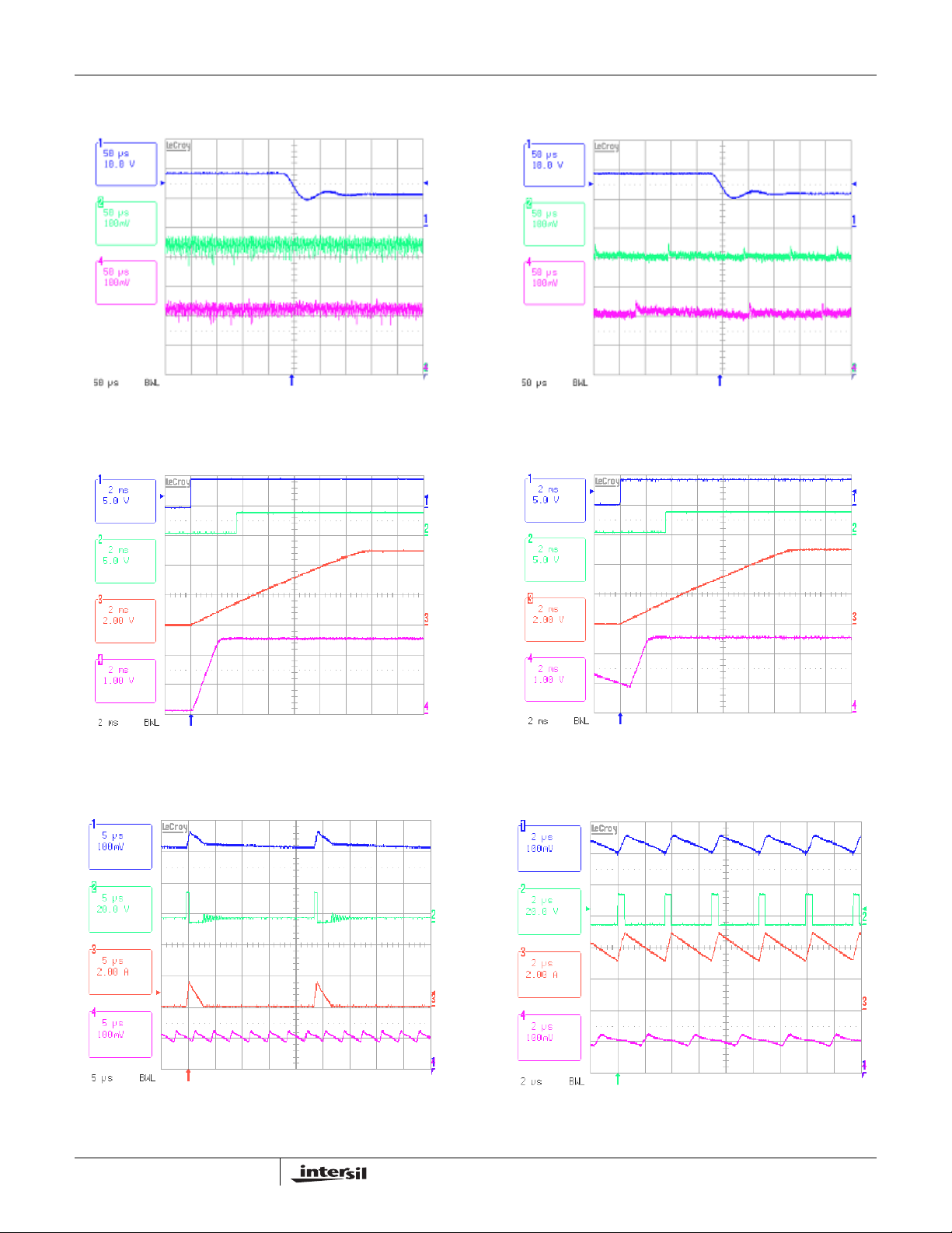
Vo1
Vphase1
Ilo1
Vo2
FIGURE 7. LOAD TRANSIENT (0 - 3A AT CHANNEL 1)
(DIODE EMULATION MODE)
Vo1
Vphase2
Vo1
Vphase1
Ilo1
Vo2
FIGURE 8. LOAD TRANSIENT (0 - 3A AT CHANNEL 1)
(FORCED PWM MODE)
Vo1
Vphase2
Ilo2
Vo2
FIGURE 9. LOAD TRANSIENT (0 - 2A AT CHANNEL 2)
(DIODE EMULATION MODE)
Vin1
Vo1
Vo2
Ilo2
Vo2
FIGURE 10. LOAD TRANSIENT (0 - 3A AT CHANNEL 2)
(FORCED PWM MODE)
Vin1
Vo1
Vo2
FIGURE 11. INPUT STEP-UP TRANSIENT AT PWM MODE FIGURE 12. INPUT STEP-UP TRANSIENT AT HYS MODE
6
FN9094.4
December 21, 2006
Typical Operation Performance (Continued)
ISL6227
Vin1
Vo1
Vo2
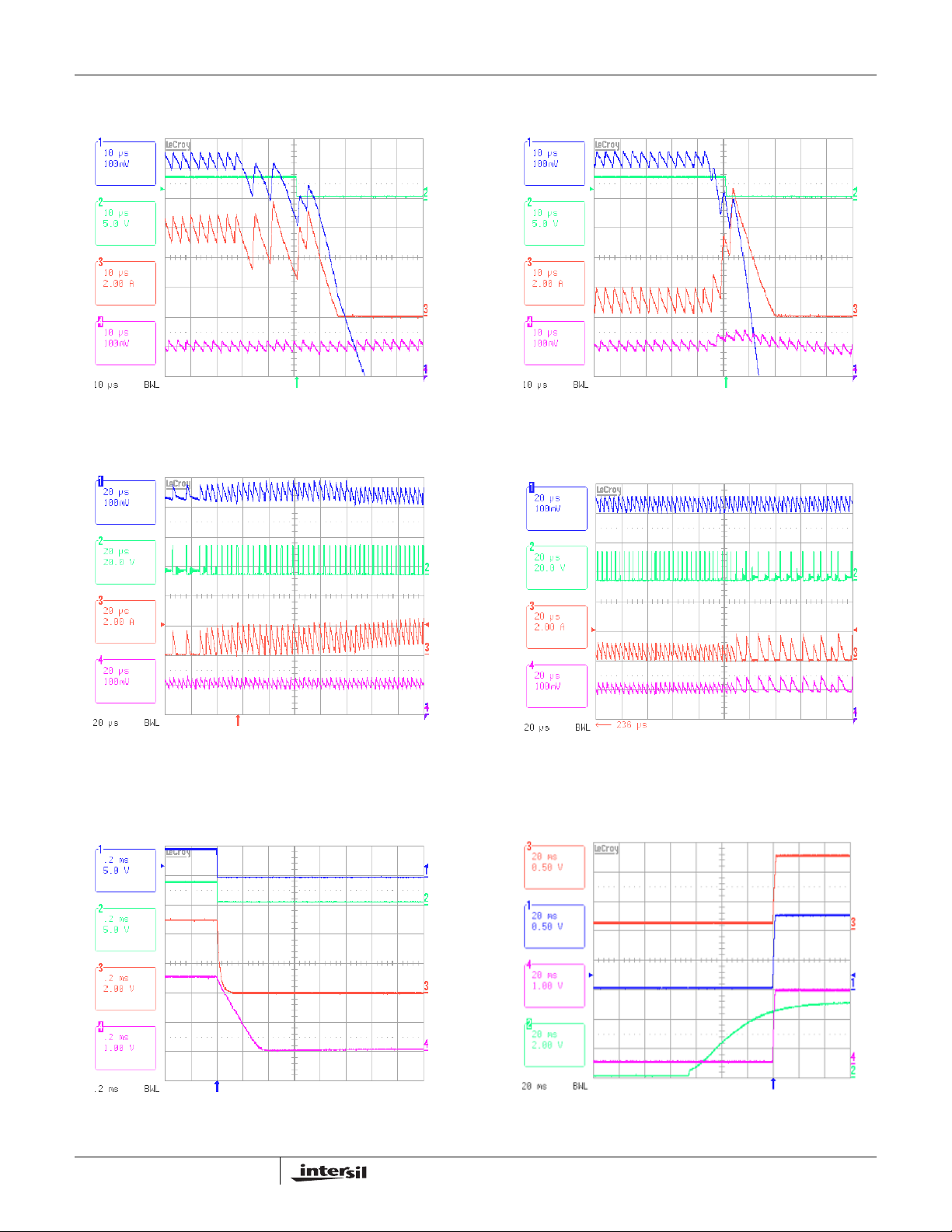
FIGURE 13. INPUT STEP-DOWN TRANSIENT AT PWM MODE FIGURE 14. INPUT STEP-DOWN TRANSIENT AT HYS MODE
EN1
PG1
Vin1
Vo1
Vo2
EN1
PG1
SOFT1
Vo1
FIGURE 15. SOFT-START INTERVAL AT ZERO INITIAL
VOLTAGE OF VO
Vo1
Vphase1
Ilo1
Vo2
SOFT1
Vo1
FIGURE 16. SOFT-ST ART INTERVAL WITH NON-ZERO INITIAL
VOLTAGE OF VO
Vo1
Vphase1
Ilo1
Vo2
FIGURE 17. OPERATION A T LIGHT LOAD OF 100mA,
CHANNEL 1
7
FIGURE 18. OPERATION AT HEAVY LOAD OF 4A,
CHANNEL 1
December 21, 2006
FN9094.4
Typical Operation Performance (Continued)
ISL6227
Vo1
PG1
Ilo1
Vo2
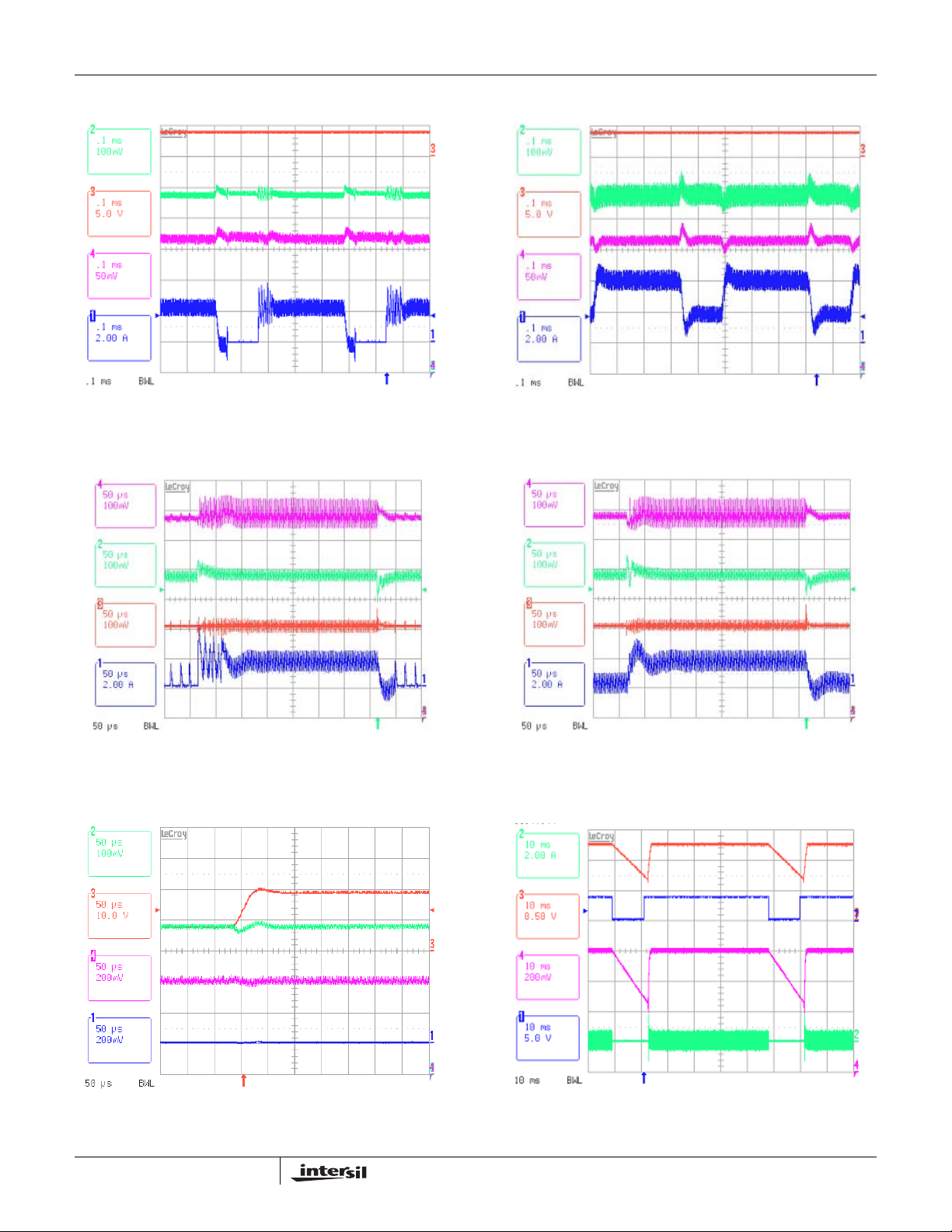
FIGURE 19. OVERCURRENT PROTECTION AT CHANNEL 1 FIGURE 20. SHORT-CIRCUIT PROTECTION AT CHANNEL 1
Vo1
Vphase1
Vo1
PG1
Ilo1
Vo2
Vo1
Vphase2
Ilo1
Vo2
FIGURE 21. MODE TRANSITION OF HYS
EN1
PG1
SOFT1
Vo1
→ _PWM
Ilo2
Vo2
FIGURE 22. MODE TRANSITION OF PWM
VTT
OCSET
VDDQ
VCC
→ HYS
FIGURE 23. SOFT SHUTDOWN INTERVAL
8
FIGURE 24. V
POWER-UP IN DDR MODE
CC
FN9094.4
December 21, 2006
Typical Operation Performance (Continued)
ISL6227
VDDQ
PGOOD1
VTT
IL1
FIGURE 25. VIN = 19V, VDDQ 3A STEP LOAD, VTT 0A LOAD FIGURE 26. VIN = 19V, VDDQ 3A STEP LOAD, VTT 3A LOAD
VDDQ
VTT
VDDQ
PGOOD1
VTT
IL1
VDDQ
VTT
OCSET2
IL2
FIGURE 27. VIN = 19V , LOAD STEP ON VTT,
VDDQ HYS MODE, 0.14A
VDDQ
Vin
VTT
OCSET2
OCSET2
IL2
FIGURE 28. VIN = 19V, LOAD STEP ON VTT,
VDDQ PWM MODE, 0.14A
VTT
EN1
VDDQ
IL1
FIGURE 29. INPUT LINE TRANSIENT IN DDR MODE FIGURE 30. VTT FOLLOWS VDDQ, ENABLE 2 IS HIGH
9
FN9094.4
December 21, 2006

ISL6227
Functional Pin Description
GND
Signal ground for the IC.
LGATE1, LGATE2
These are the outputs of the lower MOSFET drivers.
PGND1, PGND2
These pins provide the return connection for lower gate
drivers, and are connected to sources of the lower
MOSFETs of their respective converters.
PHASE1, PHASE2
The PHASE1 and PHASE2 points are the junction points of
the upper MOSFET sources, output filter inductors, and
lower MOSFET drains. Connect these pins to the respective
converter’s upper MOSFET source.
UGATE1, UGATE2
These pins provide the gate drive for the upper MOSFETs.
BOOT1, BOOT2
These pins power the upper MOSFET drivers of the PWM
converter. Connect this pin to the junction of the bootstrap
capacitor with the cathode of the bootstrap diode. The anode
of the bootstrap diode is connected to the VCC voltage.
ISEN1, ISEN2
These pins are used to monitor the voltage drop across the
lower MOSFET for current feedback and Overcurrent
protection. For precise current detection these inputs can be
connected to the optional current sense resistors placed in
series with the source of the lower MOSFETs.
EN1, EN2
These pins enable operation of the respective converter
when high. When both pins are low, the chip is disabled and
only low leakage current is taken from VCC and VIN. EN1
and EN2 can be used independently to enable either
channel 1 or channel 2.
VOUT1, VOUT2
These pins, when connected to the converter’s respective
outputs, set the converter operating in a mixed hysteretic
mode or PWM mode, depending on the load conditions. It
also provides the voltage to the chip to clamp the PWM error
amplifier in hysteretic mode to achieve smooth HYS/PWM
transition. When connected to ground, these pins command
forced continuous conduction mode (PWM) at all load levels.
VSEN1, VSEN2
These pins are connected to the resistive dividers that set
the desired output voltage. The PGOOD, UVP, and OVP
circuits use this signal to report output voltage status.
OCSET1
This pin is a buffered 0.9V internal reference voltage. A
resistor from this pin to ground sets the overcurrent
threshold for the first controller.
SOFT1, SOFT2
These pins provide soft-start function for their respective
controllers. When the chip is enabled, the regulated 4.5µA
pull-up current source charges the capacitor connected from
the pin to ground. The output voltage of the converter follows
the ramping voltage on the SOFT pin in the soft-start
process with the SOFT pin voltage as reference. When the
SOFT pin voltage is higher than 0.9V, the error amplifier will
use the internal 0.9V reference to regulate output voltage.
In the event of undervoltage and overcurrent shutdown, the
soft-start pin is pulled down though a 2k resistor to ground to
discharge the soft-start capacitor.
DDR
When the DDR pin is low, the chip can be used as a dual
switcher controller. The output voltage of the two channels
can be programmed independently by VSENx pin resistor
dividers. The PWM signals of channel 1 and channel 2 will
be synchronized 180 degrees out-of-phase. When the DDR
pin is high, the chip transforms into a complete DDR memory
solution. The OCSET2 pin becomes an input through a
resistor divider tracking to VDDQ/2. The PG2/REF pin
becomes the output of the VDDQ/2 buffered voltage. The
VDDQ/2 voltage is also used as the reference to the error
amplifier by the second channel. The channel phase-shift
synchronization is determined by the VIN pin when DDR = 1
as described in VIN below.
VIN
This pin has multiple functions. When connected to battery
voltage, it provides battery voltage to the oscillator as a feedforward for the rejection of input voltage variation. The ramp
of the PWM comparator is proportional to the voltage on this
pin (see Table 1 and Table 2 for details). While the DDR pin
is high in the DDR application, and when the VIN pin voltage
is greater than 4.2 volt when connecting to a battery, it
commands 90°
the second channel lagging the first channel, to reduce
inter-channel interference. When the pin voltage is less than
4.2V, this pin commands in-phase channel synchronizatio n.
out-of-phase channel synchronization, with
PG1
PGOOD1 is an open drain output used to indicate the status
of the output voltage. This pin is pulled low when the first
channel output is out of -11% to +15% of the set value.
10
FN9094.4
December 21, 2006

ISL6227
PG2/REF
This pin has a double function, depending on the mode of
operation.
When the chip is used as a dual channel PWM controller
(DDR = 0), the pin provides an open drain PGOOD2 function
for the second channel the same way as PG1. The pin is
pulled low when the second channel output is out of
-11% to +15% of the set value.
In DDR mode (DDR = 1), this pin is the output of the buffer
amplifier that takes VDDQ/2 voltage applied to OCSET2 pin
from the resister divider. It can source a typical 10mA
current.
OCSET2
In a dual channel application with DDR = 0, a resistor from
this pin to ground sets the overcurrent threshold for the
second channel controller. Its voltage is the buffered internal
0.9V reference.
In the DDR application with DDR = 1, this pin connects to the
center point of a resistor divider tracking the VDDQ/2. This
voltage is then buffered by an amplifier voltage follower and
sent to the PG2/REF pin. It sets the reference voltage of
channel 2 for its regulation.
Typical Application
Figures 31 and 32 show the application circuits of a dual
channel DC/DC converter for a notebook PC.
The power supply in Figure 31 provides +2.5V and +1.8V
voltages for memory and the graphics interface chipset from
a +5.0-24VDC battery voltage.
Figure 32 illustrates the application circuit for a DDR memory
power solution. The power supply shown in Figure 32
generates +2.5V VDDQ voltage from a battery. The +1.25V
VTT termination voltage tracks VDDQ/2 and is derived from
+2.5V VDDQ. To complete the DDR memory power
requirements, the +1.25V reference voltage is provided
through the PG2 pin.
VCC
This pin powers the controller.
11
FN9094.4
December 21, 2006

V1 (2.5V)
Rfb11
17.8k
Cfb1
µ
0.01 F
Rfb12
Rfb12
10k
10k
Co11
220 F
220 F
ISL6227
V
IN
Cdc
Cdc
4.7µF
D1
BAT54W
Cin1
Cin1
10 F
10 F
µ
Lo1
4.7µH
Co12
F
4.7
µ
µ
Csoft1
Csoft1
0.01 F
0.01 F
Cb
Cbt1
0.15µF
Q1
Q1
FDS6912A
FDS6912A
µ
Rbt1
0Ω
Rs1
2.0k
Rset1
100k
VIN
GND
BOOT1
UGATE1
PHASE1
ISEN1
LGATE1
PGND1
VOUT1
VSEN1
PG1
EN1
SOFT1
OCSET1
VCC
U1
U1
ISL6227
DDR
BOOT2
UGATE2
PHASE2
ISEN2
LGATE2
PGND2
VOUT2
VSEN2
PG2
EN2
SOFT2
OCSET2
Rset2
100k
Rbt2
0Ω
Rs2
2.0k
D2
BAT54W
Cbt2
Cbt2
0.15µF
Q2
Q2
FDS6912A
FDS6912A
Csoft2
0.01µF
VCC (5V)
VCC (5V)
Cin2
Cin2
10µF
Lo2
Lo2
4.7µH
Co21
Co21
220 µF
V2 (1.8V)
V
Co22
µF
4.7
Rfb21
10k
Rfb22
10k
Cfb2
µF
0.01
FIGURE 31. TYPICAL APPLICATION CIRCUIT AS DUAL SWITCHER, VOUT1 = 2.5V, VOUT = 1.8V
VDDQ (2.5V)
VDDQ (2.5V)
Cfb1
Cfb1
0.01 F
0.01µ F
Rfb1
Rfb1
17.8k
Rfb12
Rfb12
10K
Co13
Co13
220 F
220 F
Vin
Vin
Cdc
Cdc
µ
4.7 F
4.7 F
D1
BAT54W
Cin1
Cin1
10 F
10 F
µ
Lo1
Lo1
4.6 H
4.6µ H
Co11
Co11
4.7 F
4.7 F
µ
µ
Cbt1
0.15µF
Q1
Q1
FDS6912A
FDS6912A
Csoft1
0.01µF
Rbt1
0Ω
Rs1
Rs1
2.0k
Rset1
100k
GND
BOOT1
UGATE1
PHASE1
ISEN1
LGATE1
PGND1
VOUT1
VSEN1
PG1
EN1
SOFT1
OCSET1
VCC
VCC
UGATE2
PHASE2
LGATE2
LGATE2
PG2_REF
PG2_REF
U1
U1
ISL6227
VIN
VIN
DDR
DDR
BOOT2
ISEN2
PGND2
PGND2
VSEN2
VSEN2
VOUT2
VOUT2
EN2
EN2
SOFT2
SOFT2
Rs2
1.0k
OCSET2_VDDQ/2
Rbt2
0Ω
D2
BAT54W
Cbt2
0.15µF
FDS6912A
Csoft2 (N/U)
0.01µF
Q2
Q2
VDDQ
Lo2
1.5µH
1.5
Co21
220µF
Vref
Cref
4.7µF
Cf
Cf
0.1
0.1µF
VCC (5V)
VCC (5V)
Cin2
4.7µF
(VDDQ/2)
Rd1
10k
VDDQ/2
Rd2
10k
VTT (1.25V)
Co22
4.7µF
VDDQ
FIGURE 32. TYPICAL APPLICATION AS DDR MEMORY POWER SUPPLY, VDDQ = 2.5V, VTT = 1.25V
12
FN9094.4
December 21, 2006

Block Diagram
13
BOOT1
UGATE1
PHASE1
PGND1
LGATE1
VCC
MODE CHANGE COMP 1
HYSTERETIC COMPARATOR 1
+
140Ω
300kΩ
0.9V
REF
CURRENT
SAMPLE
VSEN1
SOFT1
ISEN1
OCSET1
ADAPTIVE DEAD-TIME
DIODE EMULATION
V/I SAMPLE TIMING
PWM/HYS TRANSITION
SAME STATE FOR
8 CLOCK CYCLES
REQUIRED TO CHANGE
PWM OR HYS MODE
1MΩ
500kΩ
1.25pF
ERROR AMP 1
0.9V REFERENCE
+
ΔV
HYS
CURRENT
SAMPLE
=15mV
15pF
4.4kΩ
PG1
OV UV
PGOOD
VOLTS/SEC
CLAMP
VOUT1 VOUT2
PWM1
DUTY CYCLE RAMP GENERATOR
PWM CHANNEL PHASE CONTROL
DDR EN1 EN2 VIN
011
111
VCC
GNDEN1 EN2 REF/PG2
POR
ENABLE
BIAS SUPPLIES
REFERENCE
FAULT LATCH
SOFT START
DDR MODE
CONTROL
OC1 DDR
OC2
CH1 CH2
0 ⇔ 24.0V
4.2 < VIN < 24.0V
180º
90º
VIN < 4.2
BOOT2
UGATE2
DDR=0
+
0.9V
REF
140Ω
DDR=0
PHASE2
PGND2
LGATE2
VCC
ISL6227
VSEN2
SOFT2
DDR=1
ISEN2
OCSET2
DDR=1
DDR=1
DDR=0
OV UV
PGOOD
VOLTS/SEC
PWM2
CLAMP
ADAPTIVE DEAD-TIME
DIODE EMULATION
V/I SAMPLE TIMING
PWM/HYS TRANSITION
SAME STATE FOR
8 CLOCK CYCLES
REQUIRED TO CHANGE
PWM OR HYS MODE
ΔV
=15mV
HYS
15pF
4.4kΩ
1MΩ
1.25pF
ERROR AMP 2
MODE CHANGE COMP 2
HYSTERETIC COMPARATOR 2
500kΩ
300kΩ
(200kΩ, DDR=1)
φ
CURRENT
0º
CURRENT
SAMPLE
0.9V REFERENCE
SAMPLE
+
OC2OC1
December 21, 2006
1/2.9
OCSET1
FN9094.4
1/33.1
ISEN1
SAME STATE FOR
8 CLOCK CYCLES
REQUIRED TO LATCH
OVERCURRENT FAULT
VIN
DDR
VCC
SAME STATE FOR
8 CLOCK CYCLES
REQUIRED TO LATCH
OVERCURRENT FAULT
1/33.1
ISEN2
DDR VREF
BUFFER AMP
1/2.9
OCSET2
DDR VTT
REFERENCE

ISL6227
Theory of Operation
Operation
The ISL6227 is a dual channel PWM controller intended for
use in power supplies for graphic chipsets, SDRAM, DDR
DRAM, or other low voltage power applications in modern
notebook and sub-notebook PCs. The IC integrates two
control circuits for two synchronous buck converters. The
output voltage of each controller can be set in the range of
0.9V to 5.5V by an external resistive divider.
The synchronous buck converters can operate from either
an unregulated DC source, such as a notebook battery, with
a voltage ranging from 5.0V to 24V, or from a regulated
system rail of 3.3V or 5V. In either operational mode the
controller is biased from the +5V source.
The controllers operate in the current mode with input
voltage feed-forward which simplifies feedback loop
compensation and rejects input voltage variation. An
integrated feedback loop compensation dramatically
reduces the number of external components.
Depending on the load level, converters can operate either
in a fixed 300kHz frequency mode or in a HYS mode.
Switch-over to the HYS mode of operation at light loads
improves converter efficiency and prolongs battery life. The
HYS mode of operation can be inhibited independently for
each channel if a variable frequency operation is not
desired.
The ISL6227 has a special means to rearrange its internal
architecture into a complete DDR solution. When the DDR
pin is set high, the second channel can provide the capability
to track the output voltage of the first channel. The buffered
reference voltage required by DDR memory chips is also
provided.
Initialization
The ISL6227 initializes if at least one of the enable pins is
set high. The Power-On Reset (POR) function continually
monitors the bias supply voltage on the VCC pin, and
initiates soft-start operation when EN1 or EN2 is high after
the input supply voltage exceeds 4.45V. Should this voltage
drop lower than 4.14V, the POR disables the chip.
Soft-Start
When soft-start is initiated, the voltage on the SOFT pin of
the enabled channel starts to ramp up gradually with the
internal 4.5
output voltage follows the soft-start voltage with the
converter operating at 300kHz PWM switching frequency.
μA current charging the soft-start capacitor. The
When the SOFT pin voltage reaches 0.9V, the output volt age
comes into regulation, (see block diagram). When the SOFT
voltage reaches 1.5V, the power good (PGOOD) and the
mode control is enabled. The soft-start process is depicted in
Figure 33.
1
2
3
4
Ch1 5.0V
Ch3 1.0V
EN
1.5V
0.9V
PGOOD
SOF T
VOUT
Ch2 2.0V
Ch4 5.0V
FIGURE 33. START-UP
M1.00ms
Even though the soft-start pin voltage continues to rise after
reaching 1.5V, this voltage does not affect the output
voltage. During the soft-start, the converter always operates
in continuous conduction mode independent of the load level
or VOUT pin connection.
The soft-start time (the time from the moment when EN
becomes high to the moment when PGOOD is reported) is
determined by the following equation:
T
SOFT
----------------------------------
=
4.5μ A
(EQ. 1)
1.5V Csoft×
The time it takes the output voltage to come into regulation
can be obtained from the following equation.
0.6 T
T
RISE
×=
SOFT
(EQ. 2)
During soft-start stage before the PGOOD pin is ready, the
undervoltage protection is prohibited. The overvoltage and
overcurrent protection functions are enabled.
If the output capacitor has residue voltage before startup,
both lower and upper MOSFETs are in off-state until the softstart capacitor charges equal the VSEN pin voltage. This will
ensure the output voltage starts from its existing voltage
level.
14
FN9094.4
December 21, 2006
ISL6227
Output Voltage Program
The output voltage of either channel is set by a resistive divider
from t h e o u t put to ground. The center point of the divider is
connected to the VSEN pin as shown in Figure 34. The
output voltage value is determined by the following equation.
0.9V R1 R2+()•
----------------------------------------------
V
=
O
R2
(EQ. 3)
where 0.9V is the value of the internal reference. The VSEN
pin voltage is also used by the controller for the power good
function and to detect undervoltage and overvoltage
conditions.
V
IN
Q1
UGATE
LGATE
ISL6227
FIGURE 34. OUTPUT VOLTAGE PROGRAM
OCSET
ISEN
VOUT
VSEN
Q2
R
CS
L1
C1
R
OC
V
O
C
Z
R1
R2
Operation Mode Control
VOUTx pin programs the two channels of ISL6227 in two
different operational modes:
1. If VOUTx is connected to ground, the channel will be put
into a fixed switching frequency of 300kHz CCM, also
known as forced PWM mode regardless of load
conditions.
2. If the VOUTx is connected to the output voltage, the
channel will operate in either fixed 300kHz PWM mode or
HYS mode, depending on the load conditions. It operates
in the PWM mode when the load current exceeds the
critical discontinuous conduction value, otherwise it will
operate in a HYS mode, as shown in the following table.
INDUCTOR
VOUT PIN
GND Any value Forced PWM
Connects to output voltage ≤ I
Connects to output voltage >I
CURRENT
HYS
HYS1
OPERATION
MODE
HYS
PWM
The two channels can be programmed to operate in different
modes depending on the VOUTx connection and the load
current. Once both channels operate in the PWM mode,
however, they will be synchronized to the 300kHz switching
clock. The 180° phase shift reduces the noise couplings
between the two channels and reduces the input current ripple.
The critical discontinuous conduction current value for the
PWM to HYS mode switch-over can be calculated by the
following expression.
VINVO–()VO•
I
----------------------------------------------------
=
HYS
2F
SWLOVIN
•••
The HYS mode to PWM switch-over current I
HYS1
(EQ. 4)
is
determined by the activation time of the HYS mode
controller. It is affected by the ESR, the inductor value, the
input and output voltage.
The HYS mode control can improve converter efficiency with
reduced switching frequency. The efficiency is further
improved by the diode emulat i o n sch eme in discontinuous
conduction mode. The diode emulation scheme does not
allow the inductor sink current from the output capacitor,
thereby reducing the circulating energy. It is achieved by
sensing the free-wheeling current going through the
synchronous MOSFET through Phase node voltage polarity
change after the upper MOSFET is turned off. Before the
current reverses direction, the lower MOSFET gate pulses
are terminated.
The PWM-HYS and HYS-PWM switch-over is provided
automatically by the mode control circuit, which constantly
monitors the inductor current through phase voltage polarity,
and alters the way the gate driver pulse signal is generated.
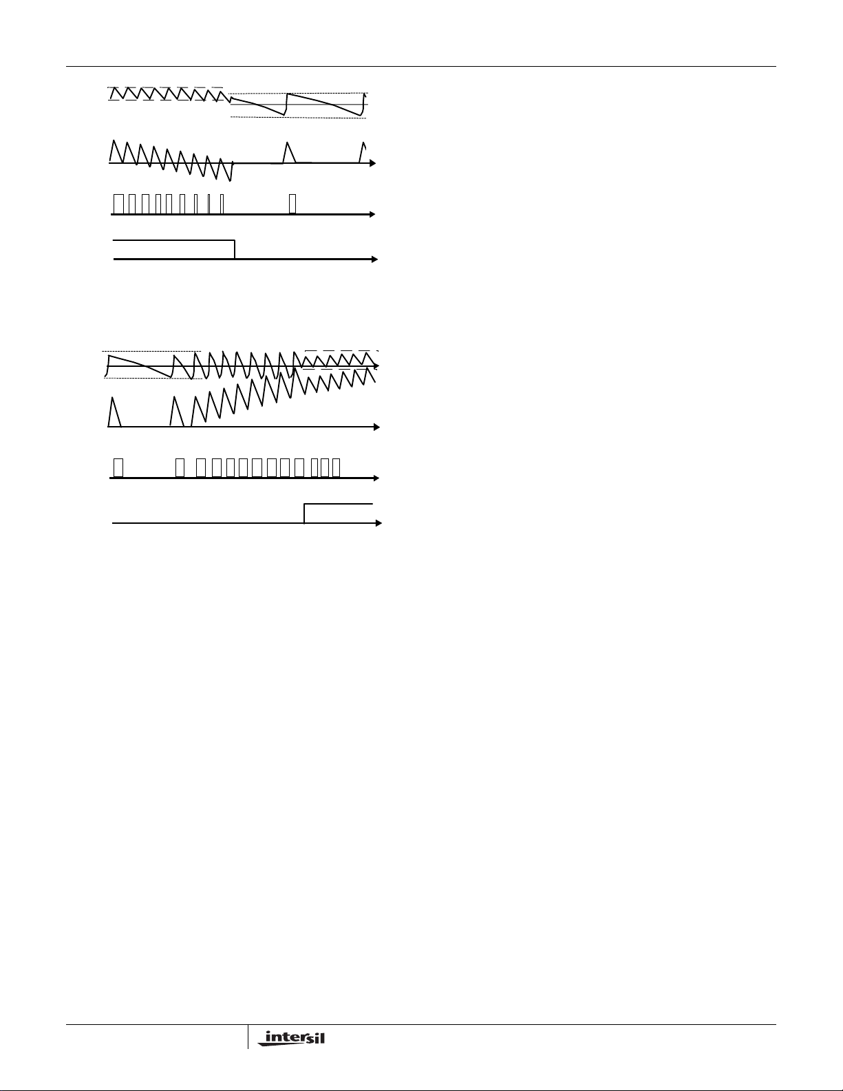
Mode Transition
For a buck regulator, if the load current is higher than critical
value I
in the free-wheeling period is always negative, and vice
versa. The mode control circuit monitors the phase node
voltage in the off-period. The polarity of this voltage is used
as the criteria for whether the load current is greater than the
critical value, and thus determines whether the converter will
operate in PWM or HYS mode.
To prevent chatter between operating modes, the circuit
looks for eight sequentially matching polarity signals before it
decides to perform a mode change. The algorithm is true for
both CCM-HYS and HYS-CCM transitions.
In the HYS mode, the PWM comparator and the error
amplifier, that provided control in the CCM mode, are put in a
clamped stage and the hysteretic comparator is activated. A
change is also made to the gate logic. The synchronous
MOSFET is controlled in diode emulation fashion, hence the
current in the synchronous MOSFET will be kept in one
direction only. Figures 35 and 36 illustrate the mode change
by counting eight switching cycles.
, the voltage drop on the synchronous MOSFET
HYS1
15
FN9094.4
December 21, 2006
ISL6227
VOUT
IIND
PHASE
COMP
MODE
OF
OPERA T ION
1 2 3 4 5 6 7 8
PWM
FIGURE 35. CCM—HYSTERETIC TRANSITION
Hysteretic
t
t
t
t
VOUT
IIND
PHASE
COMP
MODE
OF
OPERA T ION
FIGURE 36. HYSTERETIC—CCM TRANSITION
1 2 3 4 5 6 7 8
Hysteretic
PWM
If load current slowly increases or decreases, mode
transition will occur naturally, as described above; however,
if there is an instantaneous load current increase resulting in
a large output voltage drop before the hysteretic mode
controller responds, a comparator with threshold of 20mV
below the reference voltage will be tripped, and the chip will
jump into the forced PWM mode immediately. The PWM
controller will process the load transient smoothly.
Once the PWM controller is engaged, 8 consecutive
switching cycles of negative inductor current are required to
transition back to the hysteretic mode. In this way, chattering
between the two modes is prevented. Current sinking during
the 8 PWM switching cycle dumps energy to input,
smoothing output voltage load step-down.
As a side effect to this design, the comparator may be
triggered consistently if the ESR of the capacitor is so big
that the output ripple voltage exceeds the 20mV window,
resulting in a pure PWM pulse.
The PWM error amplifier is put in clamped voltage during the
hysteretic mode. The output voltage through the VOUT pin
and the input voltage through the VIN pin are used to
determine the error amplifier output voltage and the duty
cycle. The error amplifier stays in an armed state while
t
t
t
t
waiting for the transition to occur. The transition decision
point is aligned with the PWM clock. When the need for
transition is detected, there is a 500ns delay between the
first/last pulse of the PWM controller from the last/first pulse
of the hysteretic mode controller.
Current Sensing
The current on the lower MOSFET is sensed by measuring
its voltage drop within its on-time. In order to activate the
current sampling circuitry, two conditions need to be met.
(1) the Lgate is high and (2) the phase pin sees a negative
voltage for regular buck operation, which means the current
is freewheeling through lower MOSFET. For the second
channel of the DDR application, the phase pin voltage needs
to be higher than 0.1V to activate the current sensing circuit
for bidirectional current sensing. The current sampling
finishes at about 400ns after the lower MOSFET has turned
on. This current information is held for current mode control
and overcurrent protection. The current sensing pin can
source up to 260µA. The current sense resistor and OCSET
resistor can be adjusted simultaneously for the same
overcurrent protection level, however, the current sensing
gain will be changed only according to the current sense
resistor value, which will affect the current feedback loop
gain. The middle point of the Isen current can be at 75µA,
but it can be tuned up and down to fit application needs.
If another channel is switching at the moment the current
sample is finishing, it could cause current sensing error and
phase voltage jitter. In the design stage, the duty cycles and
synchronization have to be analyzed for all the input voltage
and load conditions to reduce the chance of current sensing
error. The relationship between the sampled current and
MOSFET current is given by:
I
SENRCS
140+()r
= (EQ. 5)
DS ON()ID
Which means the current sensing pin will source current to
make the voltage drop on the MOSFET equal to the voltage
generated on the sensing resistor, plus the internal resistor,
along the ISEN pin current flowing path.
Feedback Loop Compensation
Both channel PWM controllers have internally compensated
error amplifiers. To make internal compensation possible
several design measures were taken.
• The ramp signal applied to the PWM comparator has been
made proportional to the input voltage by the VIN pin. This
keeps the product of the modulator gain and the input
voltage constant even when the input voltage varies.
• The load current proportional signal is derived from the
voltage drop across the lower MOSFET during the PWM
off time interval, and is subtracted from the error amplifier
output signal before the PWM comparator input. This
effectively creates an internal current control loop.
16
FN9094.4
December 21, 2006
ISL6227
The resistor connected to the ISEN pin sets the gain in the
current sensing. The following expression estimates the
required value of the current sense resistor, depending on
the maximum continuous load current, and the value of the
MOSFETs r
, assuming the ISEN pin sources 75µA
DS(ON)
current.
I
•
MAXrDS ON()
------------------------------------------
R
= 140Ω–
CS
75μ A
(EQ. 6)
Because the current sensing circuit is a sample-and-hold
type, the information obtained at the last moment of the
sampling is used. This current sensing circuit samples the
inductor current very close to its peak value. The current
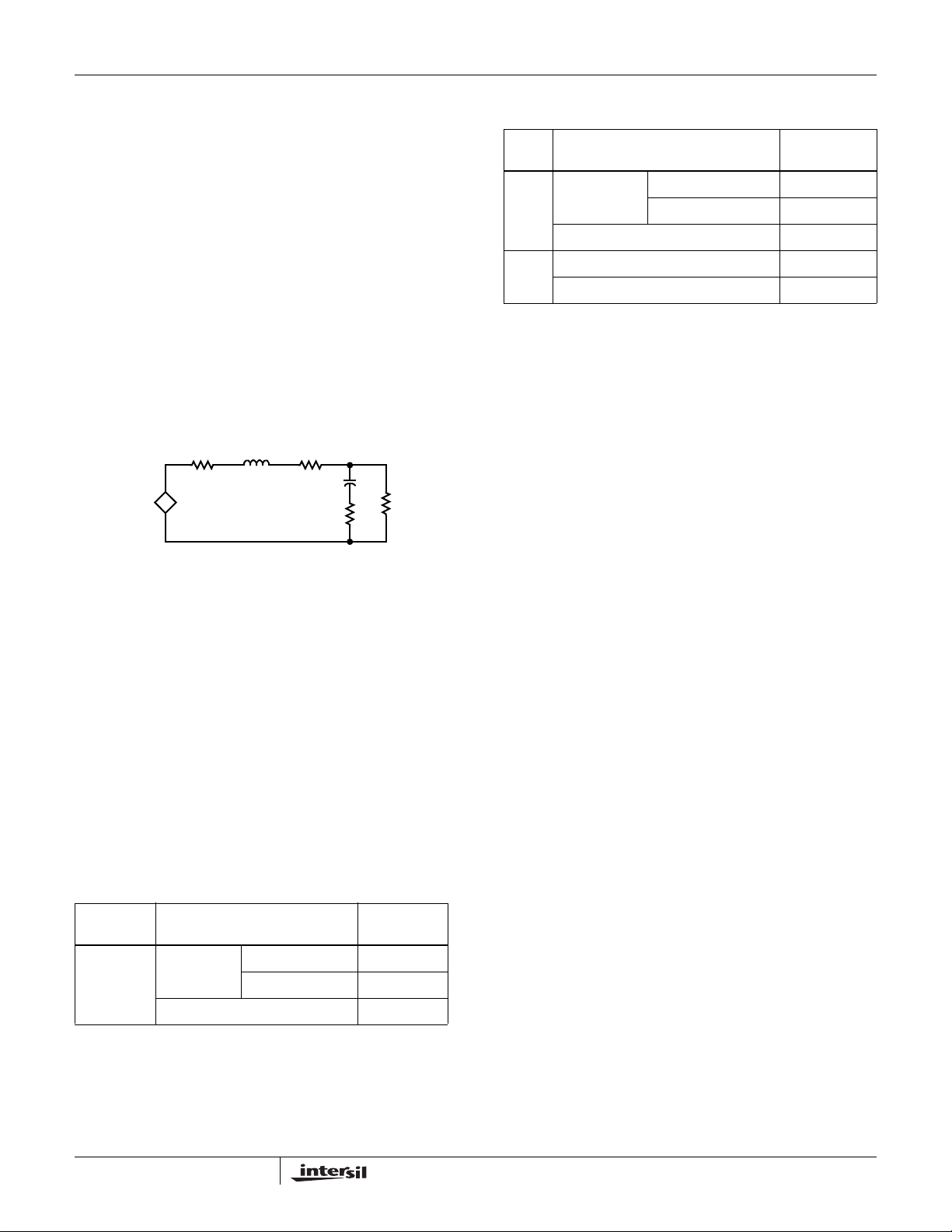
feedback essentially injects a resistor R
in series with the
i
original LC filter as shown in Figure 37, where the sampleand-hold effect of the current loop has been ignored. Vc and
Vo are small signal components extracted from its DC
operation points.
Ri Lo DCR
+
Ro Vo
-
Gm*Vc
Co
+
-
ESR
TABLE 2. PWM COMP ARA TOR RAMP VOL TAGE AMPLITUDE
FOR DDR APPLICATION
VIN PIN CONNECTION
Ch1 Input Voltage Input voltage >4.2V Vin/8
Input voltage <4.2V 1.25V
GND 1.25V
Ch2 Input voltage >4.2V 0.625V
GND 1.25V
VRAMP
AMPLITUDE
The small signal transfer function from the error amplifier
output voltage V
to the output voltage Vo can be written in
c
the following expression:
s
⎛⎞
-------- -
1+
⎝⎠
Wz
s
⎛⎞
------------ -
1+
⎝⎠
Wp2
1+
(EQ. 8)
Gs() G
=
R
---------------------------------------
m
RiDCR R
++
o
---------------------------------------------------------
s
⎛⎞
o
------------ -
⎝⎠
Wp1
The dc gain is derived by shorting the inductor and opening
the capacitor. There is one zero and two poles in this transfer
function. The zero is related to ESR and the output
capacitor.
FIGURE 37. THE EQUIVALENT CIRCUIT OF THE POWER
STAGE WITH CURRENT LOOP INCLUDED
The value of the injected resistor can be estimated by:
r
V
IN
-----------------
R
i
V
R
is in kΩ, and RDS and R
i
V
ramp
DS ON()
ramp
----------------------------
R
CS
4.4kΩ•=
140+
are in Ω . VIN divided by
CS
, is defined as Gm, which is a constant 8 or 18 dB for
both channels in dual switcher applications, when V
(EQ. 7)
is
IN
above 3V . Refer to Table 1 for the ramp amplitude in different
V
pin connections. The feed-forward effect of the VIN is
IN
reflected in Gm. V
is defined as the error amplifier output
c
voltage.
TABLE 1. PWM COMP ARATOR RAMP AMPLITUDE FOR
DUAL SWITCHER APPLICATION
VRAMP
VIN PIN CONNECTIONS
Ch1 and Ch2 Input Voltage Input voltage >4.2V Vin/8
Input voltage <4.2V 1.25V
GND 1.25V
AMPLITUDE
The first pole is a low frequency pole associated with the
output capacitor and its charging resistors. The inductor can
be regarded as short. The second pole is the high frequency
pole related to the inductor. At high frequency the output
capacitor can be regarded as a short circuit. By
approximation, the poles and zero are inversely proportional
to the time constants, associated with inductor and capacitor,
by the following expressions:
Wz
Wp1
Wp2
ESR*C
o
------------------------------------------------------------------------------ -
=
ESR R
DCR ESR++ R
R
i
----------------------------------------------------------
=
1
+()*C
i
L
o
||
DCR+()R
||
o
o
o
(EQ. 9)
(EQ. 10)
(EQ. 11)
1
----------------------- -
=
Since the current loop separates the LC resonant poles into
two distant poles, and ESR zero tends to cancel the high
frequency pole, the second order system behaves like a first
order system. This control method simplifies the design of
the internal compensator and makes it possible to
accommodate many applications having a wide range of
parameters.
17
FN9094.4
December 21, 2006
ISL6227
The schematics for the internal compensator is shown in
Figure 38.
1.25pF
TO PWM
COMPARATOR
4.4K
ISEN
FIGURE 38. THE INTERNAL COMPENSATOR
1M 15pF
Vc
500K
-
+
300K
0.9V
VSEN
Its transfer function can be written as the following:
5
Gcomp s()
s
⎛⎞
1.857 10
-------------------------------------------------------------------------------------------- -
=
---------------
•
⎝⎠
2π f
z1
s
⎛⎞
---------------
s
⎝⎠
2π f
p1
s
⎛⎞
---------------
1+
⎝⎠
1+
2π f
1+
z2
(EQ. 12)
where
f
= 6.98kHz, f
z1
= 380kHz, and f
z2
= 137kHz
p1
Outside the ISL6227 chip, a capacitor Cz can be placed in
parallel with the top resistor in the feedback resistor divider,
as shown in Figure 34. In this case th e transfer fu nction from
the output voltage to the middle point of the divider can be
written as:
Gfd s()
R1R2+
---------------------
=
The ratio of R
R
sR
2
--------------------------------------------- -
()C
sR
1R2
and R2 is determined by the output voltage
1
1Cz
||
1+
1+
z
(EQ. 13)
set point; therefore, the position of the pole and zero
frequency in the above equation may not be far apart;
however, they can improve the loop gain and phase margin
with the proper design.
The C
can bring the high frequency transient output voltage
z
variation directly to the VSEN pin to cause the PGOOD drop.
Such an effect should be considered in the selection of C
.
z
From the analysis above, the system loop gain can be
written as:
Gloop s() Gs() Gcomp s()• Gfd•= s()
(EQ. 14)
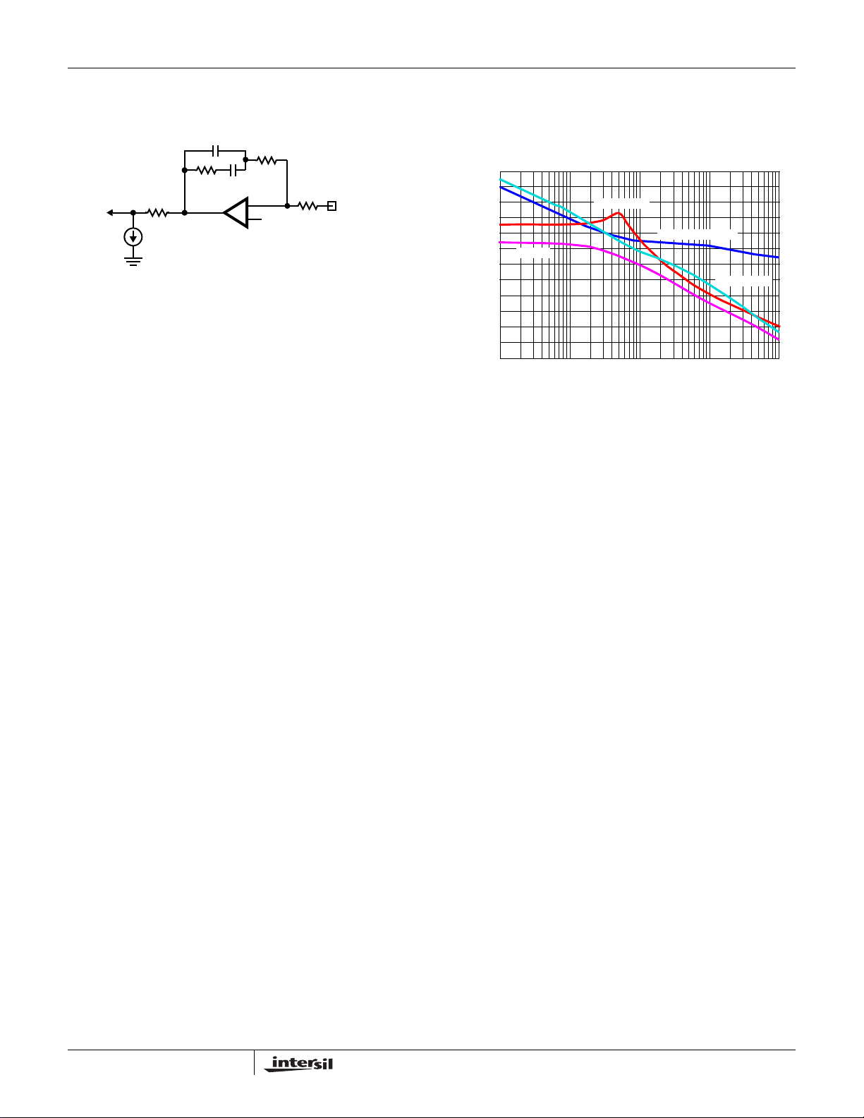
Figure 39 shows the composition of the system loop gain. As
shown in the graph, the power stage becomes a well
damped second order system as compared to the LC filter
characteristics. The ESR zero is so close to the high
frequency pole that they cancel each other out. The power
stage behaves like a first order system. With an internal
compensator, the loop gain transfer function has a cross
over frequency at about 30kHz. With a given set of
parameters, including the MOSFET r
DS(ON)
, current sense
resistor R
, output LC filter, and voltage feedback network,
CS
the system loop gain can be accurately analyzed and
modified by the system designers based on the application
requirements.
60
50
40
30
20
10
VO/VC
0
-10
GAIN (dB)
-20
-30
-40
-50
-60
100 1•10
FIGURE 39. THE BODE PLOT OF THE LC FILTER,
COMPENSATOR, CONTROL TO OUTPUT
VOLTAGE TRANSFER FUNCTION, AND SYSTEM
LOOP GAIN
LC FILTER
3
FREQUENCY (Hz)
COMPENSATOR
4
1•10
LOOP GAIN
5
1•10
1•10
Gate Control Logic
The gate control logic translates generated PWM signals
into gate drive signals providing necessary amplification,
level shift, and shoot-through protection. It bears some
functions that help to optimize the IC performance over a
wide range of the operational conditions. As MOSFET
switching time can vary dramatically from type to type, and
with the input voltage, the gate control logic provides
adaptive dead time by monitoring real gate waveforms of
both the upper and the lower MOSFETs.
Dual-Step Conversion
The ISL6227 dual channel controller can be used either in
power systems with a single-stage power conversion, when
the battery power is converted into the desired output
voltage in one step, or in the systems where some
intermediate voltages are initially established. The choice of
the approach may be dictated by the overall system design
criteria, or the approach may be a matter of voltages
available to the system designer, as in the case of PCI card
applications.
When the output voltage is regulated from low voltage such
as 5V, the feed-forward ramp may become too shallow,
creating the possibility of duty-factor jitter; this is particularly
relevant in a noisy environment. Noise susceptibility, when
operating from low level regulated power sources, can be
improved by connecting the VIN pin to ground, by which the
feed-forward ramp generator will be internally reconnected
from the VIN pin to the VCC pin, and the ramp slew rate will
be doubled.
6
18
FN9094.4
December 21, 2006

A
Ω
ISL6227
Voltage Monitor and Protections
The converter output is monitored and protected against
extreme overload, short circuit, overvoltage, and
undervoltage conditions. A sustained overload on the output
sets the PGOOD low and latches off the offending channel of
the chip. The controller operation can be restored by cycling
the VCC voltage or toggling both enable (EN) pins to low to
clear the latch.
Power Good
In the soft-start process, the PGOOD is established after the
soft pin voltage is at 1.5V. In normal operation, the PGOOD
window is 100mV below the 0.9V and 135mV higher than
0.9V. The VSEN pin has to stay within this window for
PGOOD to be high. Since the VSEN pin is used for both
feedback and monitoring purposes, the output voltage
deviation can be coupled directly to the VSEN pin by the
capacitor in parallel with the voltage divider as shown in
Figure 4. In order to prevent false PGOOD drop, capacitors
need to parallel at the output to confine the voltage deviation
with severe load step transient. The PGOOD comparator
has a built-in 3µs filter. PGOOD is an open drain output.
Overcurrent Protection
In dual switcher application, both PWM controllers use the
lower MOSFETs on-resistance r
DS(ON),
current for protection against shorted outputs. The sensed
current from the ISEN pin is compared with a current set by
a resistor connected from the OCSET pin to ground:
10.3V
R
where, I
R
---------------------------------------------------------
=
SET
is the value of the current sense resistor conne cte d to
CS
•
I
OCrDS ON()
--------------------------------------
R
140Ω+
CS
is a desired overcurrent protection threshold and
OC
8μ A+
the ISEN pin. The 8µA is the offset current added on top of
the sensed current from the ISEN pin for internal circuit
biasing.
If the lower MOSFET current exceeds the overcurrent
threshold, a pulse skipping circuit is activated. The upper
MOSFET will not be turned on and the lower MOSFET
keeps conducting as long as the sampled current is higher
than the threshold value, limiting the current supplied by the
DC voltage source. The current in the lower MOSFET will be
sampled at the internal 300kHz oscillator frequency and
monitored. When the sampled current is lower than the OC
threshold value, the following UGATE pulse will be released
and it allows turning on the upper MOSFET based on the
voltage regulation loop. This kind of operation remains for
eight clock cycles after the overcurrent comparator was
tripped for the first time. If after the first eight clock cycles the
sampled current exceeds the overcurrent threshold again,
within a time interval of another eight clock cycles, the
overcurrent protection latches and disables the offending
channel. If the overcurrent condition goes away during the
to monitor the
(EQ. 15)
first eight clock cycles, normal operation is restored and the
overcurrent circuit resets itself at the end of sixteenth clock
cycles; see Figure 40.
1
2
3
Ch3 1.0
FIGURE 40. OVERCURRENT PROTECTION
Due to the nature of the used current sensing technique,
and to accommodate a wide range of the r
the value of the overcurrent threshold should set at about
180% of the nominal load value. If more accurate current
protection is desired, a current sense resistor placed in
series with the lower MOSFET source may be used. The
inductor current going through the lower MOSFET is sensed
and held at 400ns after the upper MOSFET is turned off;
therefore, the sensed current is very close to its peak value.
The inductor peak current can be written as:
VINVo–()Vo•
peak
--------------------------------------------
2L
oFSWVIN
I
As seen from the equation above, the inductor peak current
changes with the input voltage and the inductor value once
an output voltage is selected.
After overcurrent protection is activated, there are two ways
to bring the offending channel back: (1) Both EN1 and EN2
have to be held low to clear the latch, (2) To recycle the Vcc
of the chip, the POR will clear the latch.
Undervoltage Protection
In the process of operation, if a short circuit occurs, the output
voltage will drop quickly. Before the overcurrent protection
circuit responds, the output voltage will fall out of the required
regulation range. The chip comes with undervoltage protection.
If a load step is strong enough to pull the output voltage lower
than the undervoltage threshold, the offending channel latches
off immediately . The undervoltage threshold is 75% of the
nominal output voltage. Toggling both pins to low, or recycling
Vcc, will clear the latch and bring the chip back to operation.
Overvoltage Protection
Should the output voltage increase over 115% of the normal
value due to the upper MOSFET failure, or for other reasons,
the overvoltage protection comparator will force the
synchronous rectifier gate driver high. This action actively
pulls down the output voltage and eventually attempts to
blow the battery fuse. As soon as the output voltage is within
PGOOD
I
load
8 CLK
SHUTDOWN
M 10.0μsCh1 5.0V
DS(ON)
variation,
(EQ. 16)
IL
VOUT
Ch2 100mV
+=
••
19
FN9094.4
December 21, 2006

ISL6227
regulation, the OVP comparator is disengaged. The
MOSFET driver will restore its normal operation. When the
OVP occurs, the PGOOD will drop to low as well.
This OVP scheme provides a ‘soft’ crowbar function, which
helps clamp the voltage overshoot, and does not invert the
output voltage when otherwise activated with a continuously
high output from lower MOSFET driver - a com mon prob lem
for OVP schemes with a latch.
DDR Application
High throughput Double Data Rate (DDR) memory ICs are
replacing traditional memory ICs in the latest generation of
Notebook PCs and in other computing devices. A novel
feature associated with this type of memory are the
referencing and data bus termination techniques. These
techniques employ a reference voltage, VREF, that tracks
the center point of VDDQ and VSS voltages, and an
additional VTT power source where all terminating resistors
are connected. Despite the additional power source, the
overall memory power consumption is reduced compared to
traditional termination.
The added power source has a cluster of requirements that
should be observed and considered. Due to the reduced
differential thresholds of DDR memory, the termination
power supply voltage, VTT, closely tracks VDDQ/2 voltage.
Another very important feature of the termination power
supply is the capability to operate at equal efficiency in
sourcing and sinking modes. The VTT supply regulates the
output voltage with the same degree of precision when
current is flowing from the supply to the load, and when the
current is diverted back from the load into the power supply.
The ISL6227 dual channel PWM controller possesses
several important enhancements that allow re-configuration
for DDR memory applications, and provides all three
voltages required in a DDR memory compliant computer.
To reconfigure the ISL6227 for a complete DDR solution, the
DDR pin should be set high permanently to the VCC rail.
This activates some functions inside the chip that are
specific to DDR memory power needs.
In the DDR application presented in Figure 32, the first
controller regulates the VDDQ rail to 2.5V. The output
voltage is set by external dividers Rfb1 and Rfb12. The
second controller regulates the VTT rail to VDDQ/2. The
OCSET2 pin function is now different, and serves as an
input that brings VDDQ/2 voltage, created by the Rd1 and
Rd2 divider, inside the chip, effectively providing a tracking
function for the VTT voltage.
The PG2 pin function is also different in DDR mode. This pin
becomes the output of the buffer, whose input is connected
to the center point of the R/R divider from the VDDQ output
by the OCSET2 pin. The buffer output voltage serves as a
1.25V reference for the DDR memory chips. Current
capability of this pin is 10mA (12mA max).
For the VTT channel where output is derived from the VDDQ
output, some control and protective functions have been
significantly simplified. For example, the overcurrent, and
overvoltage, and undervoltage protections for the second
channel controller are disabled when the DDR pin is set
high. The hysteretic mode of operation is also disabled on
the VTT channel to allow sinking capability to be
independent from the load level. As the VTT channel tracks
the VDDQ/2 voltage, the soft-start function is not required,
and the SOFT2 pin may be left open, in the event both
channels are enabled simultaneously. However, if the VTT
channel is enabled later than the VDDQ, the SOFT2 pin
must have a capacitor in place to ensure soft-start. In case of
overcurrent or undervoltage caused by short circuit on VTT,
the fault current will propagate to the first channel and shut
down the converter.
The VREF voltage will be present even if the VTT is
disabled.
Channel Synchronization in DDR Applications
The presence of two PWM controllers on the same die
requires channel synchronization, to reduce inter-channel
interference that may cause the duty factor jitter and
increased output ripple.
The PWM controller is at greatest noise susceptibility when
an error signal on the input of the PWM comparator
approaches the decision making point. False triggering may
occur, causing jitter and affecting the output regulation.
A common approach used to synchronize dual channel
converters is out-of-phase operation. Out-of-phase
operation reduces input current ripple and provides a
minimum interference for channels that control different
voltage levels.
When the DDR pin is connected to GND for dual switcher
applications, the channels operate 180° out-of-phase. When
used in a DDR application with cascaded converters (VTT
generated from VDDQ), several methods of synchronization
are implemented in the ISL6227. In the DDR mode, when
the DDR pin is connected to VCC, the channels operate
either with 0° phase shift, when the VIN pin is connected to
the GND, or with 90° phase shift if the VIN pin is connected
to a voltage higher than 4.2V.
The following table lists the different synchronization
schemes and their usage:
DDR PIN VIN PIN SYNCHRONIZATION
0 Vin pin >4.2V 180° out of phase
1 Vin pin voltage <4.2V 0° phase
1 Vin pin voltage >4.2V 90° phase shift
20
FN9094.4
December 21, 2006
ISL6227
Application Information
Design Procedures
GENERAL
A ceramic decoupling capacitor should be used between the
VCC and GND pin of the chip. There are three major
currents drawn from the decoupling capacitor:
1. the quiescent current, supporting the internal logic and
normal operation of the IC
2. the gate driver current for the lower MOSFETs
3. and the current going through the external diodes to the
bootstrap capacitor for upper MOSFET.
In order to reduce the noisy effect of the bootstrap capacitor
current to the IC, a small resistor, such as 10Ω, can be used
with the decoupling cap to construct a low pass filter for the
IC, as shown in Figure 41. The soft-start capacitor and the
resistor divider setting the output voltage is easy to select as
discussed in the “Block Diagram” on page 13.
TO BOOT
5V
10Ω
FIGURE 41. INPUT FILTERING FOR THE CHIP
Selection of the Current Sense Resistor
The value of the current sense resistor determines the gain
of the current sensing circuit. It affects the current loop gain
and the overcurrent protection setpoint. The voltage drop on
the lower MOSFET is sensed within 400ns after the upper
MOSFET is turned off. The current sense pin has a 140Ω
resistor in series with the external current sensing resistor.
The current sense pin can source up to a 260µA current
while sensing current on the lower MOSFET, in such a way
that the voltage drop on the current sensing path would be
equal to the voltage on the MOSFET.
I
SOURCINGRCS
I
can be assumed to be the inductor peak current. In a
D
worst case scenario, the high temperature r
increase to 150% of the room temperature level. During
overload condition, the MOSFET drain current I
130% higher than the normal inductor peak. If the inductor
has 30% peak-to-peak ripple, I
load current. The design should consider the above factors
so that the maximum I
under worst case conditions. To be safe, I
be less than 100µA in normal operation at room
temperature. The formula in the earlier discussion assumes
a 75µA sourcing current. Users can tune the sourcing
140Ω+()IDr
=
SOURCING
DS ON()
D
VCC
(EQ. 17)
could
DS(ON)
could be
D
would equal to 115% of the
will not saturate to 260µA
SOURCING
should
current of the ISEN pin to meet the overcurrent protection
and the change the current loop gain. The lower the current
sensing resistor, the higher gain of the current loop, which
can damp the output LC filter more.
A higher value current-sensing resistor will decrease the
current sense gain. If the phase node of the converter is very
noisy due to poor layout, the sensed current will be
contaminated, resulting in duty cycle jittering by the current
loop. In such a case, a bigger current sense resistor can be
used to reduce both real and noise current levels. This can
help damp the phase node wave form jittering.
Sometimes, if the phase node is very noisy, a resistor can be
put on the ISEN pin to ground. This resistor together with the
R
can divide the phase node voltage down, seen by the
CS
internal current sense amplifier, and reduce noise coupling.
Sizing the Overcurrent Setpoint Resistor
The internal 0.9V reference is buffered to the OCSET pin
with a voltage follower (refer to the equivalent circuit in
Figure 42). The current going through the external
overcurrent set resistor is sensed from the OCSET pin. This
current, divided by 2.9, sets up the overcurrent threshold and
compares with the scaled ISEN pin current going through
R
with an 8µA offset. Once the sensed current is higher
CS
than the threshold value, an OC signal is generated. The first
OC signal starts a counter and activates a pulse skipping
function. The inductor current will be continuously monitored
through the phase node voltage after the first OC trip. As
long as the sensed current exceeds the OC threshold value,
the following PWM pulse will be skipped. This operation will
be the same for 8 switching cycles. Another OC occurring
between 8 to 16 switching cycles would result in a latch off
with both upper and lower drives low. If there is no OC within
8 to 16 switching cycles, normal operation resumes.
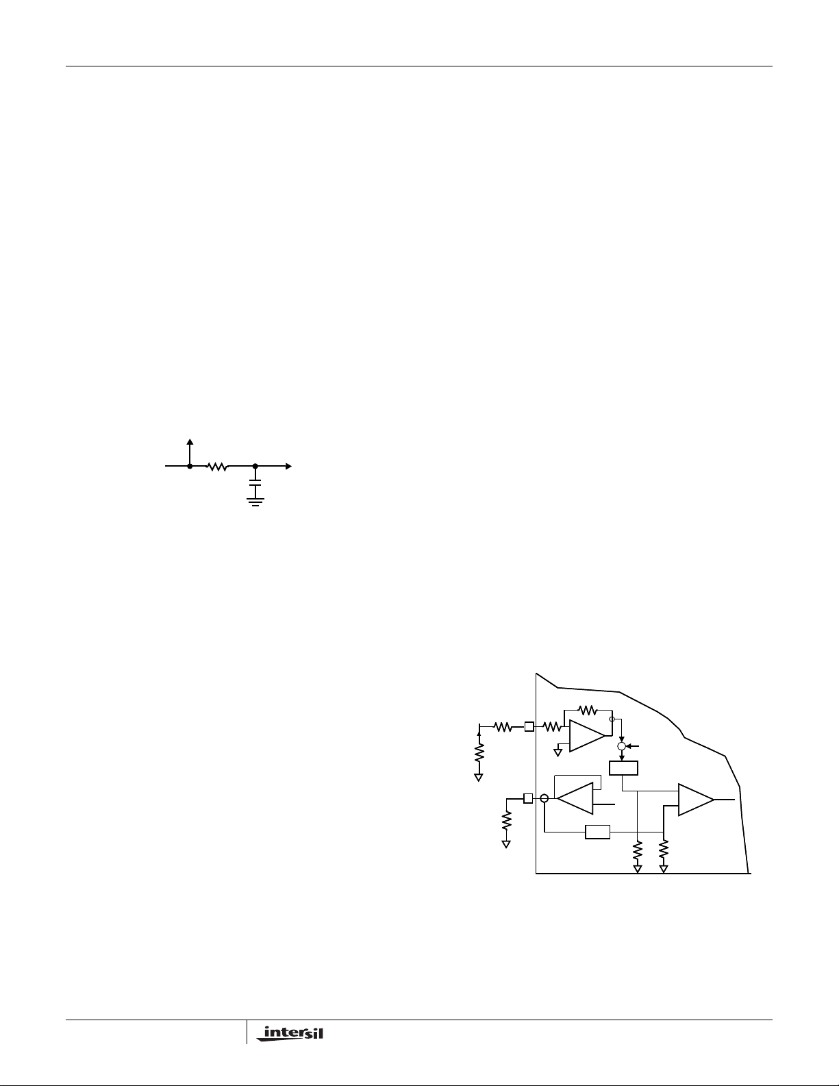
ISEN
ISEN
140 Ω
PHASE
PHASE
R
R
CS
CS
_
_
Rdson
Rdson
+
+
Rset
Rset
FIGURE 42. EQUIV ALENT CIRCUIT F OR OC SIGN AL
140 Ω
OCSET
OCSET
Amplifier
Amplifier
GENERATOR
_
_
+
+
_
_
+
+
0.9 V
0.9 V
Reference
Reference
÷ 2.9
÷ 2.9
+
+
Σ
Σ
÷ 33.1
÷ 33.1
8uA
8uA
+
+
Isense
Isense
+
+
OC
OC
_
_
Comparator
Comparator
21
FN9094.4
December 21, 2006

ISL6227
Based on the above description and functional block
diagram, the OC set resistor can be calculated as:
10.3V
---------------------------------------------------
R
=
set
I
OCrDS ON()
---------------------------------
RCS140+
I
is the inductor peak current and not the load current.
OC
8μ A+
(EQ. 18)
Since inductor peak current changes with input voltage, it is
better to use an oscilloscope when testin g th e overcurrent
setting point to monitor the inductor current, and to
determine when the OC occurs. T o get consistent test results
on different boards, it is best to keep the MOSFET at a fixed
temperature.
The MOSFET will not heat-up when applying a very low
frequency and short load pulses with an electronic load to
the output.
As an example, assume the following:
• The maximum normal operation load current is 1
• The inductor peak current is 1.15-1.3 times higher than
the load current, depending on the inductor value and the
input voltage
•The r
should set at least 1.8 to 2 times higher than the
I
OC
has a 45% increase at higher temperature
DS(ON)
maximum load current to avoid nuisance overcurrent trip.
Selection of the LC Filter
The duty cycle of a buck converter is a function of the input
voltage and output voltage. Once an output voltage is fixed,
it can be written as:
selection. Another factor to consider when choosing the
inductor is its saturation characteristics at elevated
temperature. Saturated inductors could result in nuisance
OC, or OV trip.
Output voltage ripple and the transient voltage deviation are
factors that have to be taken into consideration when
selecting an output capacitor. In addition to high frequency
noise related MOSFET turn-on and turn-off, the output
voltage ripple includes the capacitance voltage drop and
ESR voltage drop caused by the AC peak-to-peak current.
These two voltages can be represented by:
I
pp
----------------------
ΔV
c
ΔV
esrIpp
=
8CoF
sw
ESR=
(EQ. 22)
(EQ. 23)
These two components constitute a large portion of the total
output voltage ripple. Several capacitors have to be
paralleled in order to reduce the ESR and the voltage ripple.
If the output of the converter has to support another load
with high pulsating current, more capacitors are needed in
order to reduce the equivalent ESR and suppress the
voltage ripple to a tolerable level.
To support a load transient that is faster than the switching
frequency, more capacitors have to be used to reduce the
voltage excursion during load step change. Another aspect
of the capacitor selection is that the total AC current going
through the capacitors has to be less than the rated RMS
current specified on the capacitors, to prevent the capacitor
from over-heating.
V
o
IN
---------
=
V
IN
, of ISL6227 is 300kHz. The
sw
(EQ. 19)
()
DV
The switching frequency, F
peak-to-peak ripple current going through the inductor can
be written as:
Vo1DVIN()–()
-----------------------------------------
I
=
pp
F
swLo
(EQ. 20)
As higher ripple current will result in higher switching loss
and higher output voltage ripple, the peak-to-peak current of
the inductor is generally designed with a 20%-40% peak-topeak ripple of the nominal operation current. Based on this
assumption, the inductor value can be selected with the
above equation. In addition to the mechanical dimension, a
shielded ferrite core inductor with a very low DC resistance,
DCR, is preferred for less core loss and copper loss. The DC
copper loss of the inductor can be estimated by:
P
=
copperIload
2
DCR
(EQ. 21)
The inductor copper loss can be significant in the total
system power loss. Attention has to be given to the DCR
22
FN9094.4
December 21, 2006

ISL6227
Selection of the Input Capacitor
When the upper MOSFET is on, the current in the output
inductor will be seen by the input capacitor. Even though this
current has a triangular shape top, its RMS value can be
fairly approximated by:
lin
() DVIN()*I
rmsVIN
=
load
(EQ. 24)
This RMS current includes both DC and AC components.
Since the DC component is the product of duty cycle and
load current, the AC component can be approximated by:
() DVIN()DVIN()–
li
nacVIN
=
()I
2
load
(EQ. 25)
AC components will be provided from the input capacitor.
The input capacitor has to be able to handle this ripple
current without overheating and with tolerable voltage ripple.
In addition to the capacitance, a ceramic capacitor is
generally used between the drain terminal of the upper
MOSFET and the source terminal of the lower MOSFET, in
order to clamp the parasitic voltage ringing at the phase
node in switching.
Choosing MOSFETs
For a notebook battery with a maximum voltage of 24V, at
least a minimum 30V MOSFETs should be used. The design
has to trade off the gate charge with the r
MOSFET:
• For the lower MOSFET, before it is turned on, the body
diode has been conducting. The lower MOSFET driver will
not charge the miller capacitor of this MOSFET.
• In the turning off process of the lower MOSFET, the load
current will shift to the body diode first. The high dv/dt of
the phase node voltage will charge the miller capacitor
through the lower MOSFET driver sinking current path.
This results in much less switching loss of the lower
MOSFETs.
The duty cycle is often very small in high battery voltage
applications, and the lower MOSFET will conduct most of
the switching cycle; therefore, the lower the r
lower MOSFET , the less the power loss. The gate charge for
this MOSFET is usually of secondary consideration.
The upper MOSFET does not have this zero voltage
switching condition, and because it conducts for less time
compared to the lower MOSFET, the switching loss tends to
be dominant. Priority should be given to the MOSFETs with
less gate charge, so that both the gate driver loss, and
switching loss, will be minimized.
DS(ON)
DS(ON)
of the
of the
For the lower MOSFET , it s power loss can be assumed to be
the conduction loss only.
()1DVIN()–()I
P
lowerVIN
≈
2
load
r
DS ON()Lower
(EQ. 26)
For the upper MOSFET, its conduction loss can be written
as:
P
uppercondVIN
()DVIN()I
=
load
2
R
DS ON()upper
(EQ. 27)
and its switching loss can be written as:
P
upperswVIN
()
V
INIvallyTonFsw
----------------------------------------------
2
V
INIpeakToffFsw
---------------------------------------------- -
+=
2
(EQ. 28)
The peak and valley current of the inductor can be obtained
based on the inductor peak-to-peak current and the load
current. The turn-on and turn-off time can be estimated with
the given gate driver parameters in the Electrical
Specification Table on page 3. For example, if the gate driver
turn-on path of MOSFET has a typical on-resistance of 4Ω,
its maximum turn-on current is 1.2A with 5V Vcc. This
current would decay as the gate voltage increased. With the
assumption of linear current decay, the turn-on time of the
MOSFETs can be written with:
2Q
gd
---------------- -
T
=
on
I
driver
Q
is used because when the MOSFET drain-to-source
gd
(EQ. 29)
voltage has fallen to zero, it gets charged. Similarly, the turnoff time can be estimated based on the gate charge and the
gate drivers sinking current capability.
The total power loss of the upper MOSFET is the sum of the
switching loss and the conduction loss. The temperature rise
on the MOSFET can be calculated based on the thermal
impedance given on the datasheet of the MOSFET. If the
temperature rise is too much, a different MOSFET package
size, layout copper size, and other options have to be
considered to keep the MOSFET cool. The temperature rise
can be calculated by:
T
rise
θ P
=
ja totalpower loss
(EQ. 30)
The MOSFET gate driver loss can be calculated with the
total gate charge and the driver voltage Vcc. The lower
MOSFET only charges the miller capacitor at turn-off.
P
=
driverVccQgsFsw
(EQ. 31)
Based on the above calculation, the system efficiency can
be estimated by the designer.
23
FN9094.4
December 21, 2006

ISL6227
Confining the Negative Phase Node Voltage Swing
with Schottky Diode
At each switching cycle, the body diode of the lower MOSFET
will conduct before the MOSFET is turned on, as the inductor
current is flowing to the output capacitor. This will result in a
negative voltage on the phase node. The higher the load
current, the lower this negative voltage. This voltage will ring
back less negative when the lower MOSFET is turned on.
A total 400ns period is given to the current sample-and-hold
circuit on the ISEN pin to sense the current going through
the lower MOSFET after the upper MOSFET turns off. An
excessive negative voltage on the lower MOSFET will be
treated as overcurrent. In order to confine this voltage, a
schottky diode can be used in parallel with the lower
MOSFET for high load current applications. PCB layout
parasitics should be minimized in order to reduce the
negative ringing of phase voltage.
The second concern for the phase node voltage going into
negative is that the boot strap capacitor between the BOOT
and PHASE pin could get be charged higher than VCC
voltage, exceeding the 6.5V absolute maximum voltage
between BOOT and PHASE when the phase node voltage
became negative. A resistor can be placed between the
cathode of the boot strap diode and BOOT pin to increase
the charging time constant of the boot cap. This resistor will
not affect the turn-on and off of the upper MOSFET.
Schottky diode can reduce the reverse recovery of the lower
MOSFET when transition from freewheeling to blocking,
therefore, it is generally good practice to have a schottky
diode closely parallel with the lower MOSFET. B340LA, from
Diodes, Inc.®, can be used as the external schottky diode.
Tuning the Turn-on of Upper MOSFET
The turn-on speed of the upper MOSFET can be adjusted by
the resistor connecting the boot cap to the BOOT pin of the
chip. This resistor can confine the voltage ringing on the boot
capacitor from coupling to the boot pin. This resistor slows
down only the turn-on of the upper MOSFET.
If the upper MOSFET is turned on very fast, it could result in
a very high dv/dt on the phase node, which could couple into
the lower MOSFET gate through the miller capacitor,
causing momentous shoot-through. This phenomenon,
together with the reverse recovery of the body diode of the
lower MOSFET, can over-shoot the phase node voltage to
beyond the voltage rating of the MOSFET . However , a bigger
resistor will slow the turn-on of the MOSFET too much and
lower the efficiency. Trade-offs need to be made in choosing
a suitable resistor value.
System Loop Gain and Stability
The system loop gain is a product of three transfer functions:
1. the transfer function from the output voltage to the
feedback point,
2. the transfer function of the internal compensation circuit
from the feedback point to the error amplifier output voltage,
3. and the transfer function from the er ror amplifier output to
the converter output voltage.
These transfer functions are written in a closed form in the
Theory of Operation section on page 18. The external
capacitor, in p a rallel w ith the upper resisto r of the resistor
divider, C
margin. Other component parameters, such as the inductor
value, can be changed for a wider cross-over frequency of the
system loop gain. A body plot of the loop gain transfer function
with a 45 degree phase margin (a 60 degree phase margin is
better) is desirable to cover component parameter variations.
, can be used to tune the loop gain and phase
z
Testing the Overvoltage on Buck Converters
For synchronous buck converters, if an active source is used
to raise the output voltage for the overvoltage protection test,
the buck converter will behave like a boost converter and
dump energy from the external source to the input. The
overvoltage test can be done on ISL6227 by connecting the
VSEN pin to an external voltage source or signal generator
through a diode. When the external voltage, or signal
generator voltage, is tuned to a higher level than the
overvoltage threshold (the lower MOSFET will be on), it
indicates the overvoltage protection works. This kind of
overvoltage protection does not require an external schottky
in parallel with the output capacitor.
Layout Considerations
Power and Signal Layer Placement on the PCB
As a general rule, power layers should be close together,
either on the top or bottom of the board, with signal layers on
the opposite side of the board. For example, prospective
layer arrangement on a 4 layer board is shown below:
1. Top Layer: ISL6227 signal lines
2. Signal Ground
3. Power Layers: Power Ground
4. Bottom Layer: Power MOSFET, Inductors and other
Power traces
It is a good engineering practice to separate the power
voltage and current flowing path from the control and logic
level signal path. The controller IC will stay on the signal
layer, which is isolated by the signal ground to the power
signal traces.
24
FN9094.4
December 21, 2006

ISL6227
Component Placement
The control pins of the two-channel ISL6227 are located
symmetrically on two sides of the IC; it is desirable to
arrange the two channels symmetrically around the IC.
The power MOSFET should be close to the IC so that the
gate drive signal, the LGATEx, UGATEx, PHASEx, BOOTx,
and ISENx traces can be short.
Place the components in such a way that the area under the
ISL6227 has fewer noise traces with high dv/dt and di/dt,
such as gate signals and phase node signals.
Signal Ground and Power Ground Connection
At minimum, a reasonably large area of copper, which will
shield other noise couplings through the IC, could be used
as signal ground beneath the ISL6227. The best tie-point
between the signal ground and the power ground is at the
negative side of the output capacitor on each channel, where
there is less noise. Noisy traces beneath the ISL6227 are
not recommended.
GND and VCC
At least one high quality ceramic decoupling cap should be
used across these two pins. A via can tie Pin 1 to signal
ground. Since Pin1 and Pin 28 are close together, the
decoupling cap can be put close to the IC.
LGATE1 and LGATE2
These are the gate drive signals for the bottom MOSFET s of
the buck converter. The signal going through these traces
have both high dv/dt and high di/dt, with high peak charging
and discharging current. These two traces should be short,
wide, and away from other traces. There should be no other
weak signal traces in parallel with these traces on any layer.
PGND1 and PGND2
Each pin should be laid out to the negative side of the
relevant output cap with separate traces.The negative side
of the output capacitor must be close to the source node of
the bottom MOSFET. These traces are the return path of
LGATE1 and LGATE2.
PHASE1 and PHASE2
These traces should be short, and positioned away from other
weak signal traces. The phase node has a very high dv/dt w ith
a voltage swing from the input voltage to ground. No trace
should be in parallel with these traces. These traces are also
the return path for UGA TE1 and UGA TE2. Conne ct these pins
to the respective converter’s upper MOSFET source.
Pin 5 and Pin 24, the UGATE1 and UGATE2
These pins have a square shape waveform with high dv/dt. It
provides the gate drive current to charge and discharge the
top MOSFET with high di/dt. This trace should wide, short,
and away from other traces similar to the LGATEx.
BOOT1 and BOOT2
These pins di/dt are as high as that of the UGATEx;
therefore, the traces should be as short as possible.
ISEN1 and ISEN2
The ISEN trace should be a separate trace, and
independently go to the drain terminal of the lower MOSFET.
The current sense resistor should be close to ISEN pin.
The loop formed by the bottom MOSFET, output inductor,
and output capacitor, should be very small. The source of
the bottom MOSFET should tie to the negative side of the
output capacitor in order for the current sense pin to get the
voltage drop on the R
DSON
.
EN1 and EN2
These pins stay high in enable mode and low in idle mode
and are relatively robust. Enable signals should refer to the
signal ground.
VOUT1 and VOUT2
These pins connect either to the output voltage or to the
signal ground. They are signal lines and should be kept
away from noisy lines.
VSEN1 and VSEN2
There is usually a resistor divider connecting the output
voltage to this pin. The input impedance of these two pins is
high because they are the input to the amplifiers. The correct
layout should bring the output voltage from the regulation
point to the SEN pin with kelvin traces. Build the resistor
divider close to the pin so that the high impedance trace is
shorter.
OCSET1 and OCSET2
In dual switcher mode operation, the overcurrent set resistor
should be put close to this pin. In DDR mode operation, the
voltage divider, which divides the VDQQ voltage in half,
should be put very close to this pin. The other side of the OC
set resistor should connect to signal ground.
SOFT1 and SOFT2
The soft-start capacitors should be laid out close to this pin.
The other side of the soft-start cap should tie to signal ground.
PG1 and PG2/REF
For dual switcher operations, these two lines are less noise
sensitive. For DDR applications, a capacitor should be
placed to the PG2/REF pin.
DDR
This pin should connect to VCC in DDR applications, and to
signal ground in dual switcher applications.
VIN
This pin connects to battery voltage, and is less noise sensitive.
25
FN9094.4
December 21, 2006
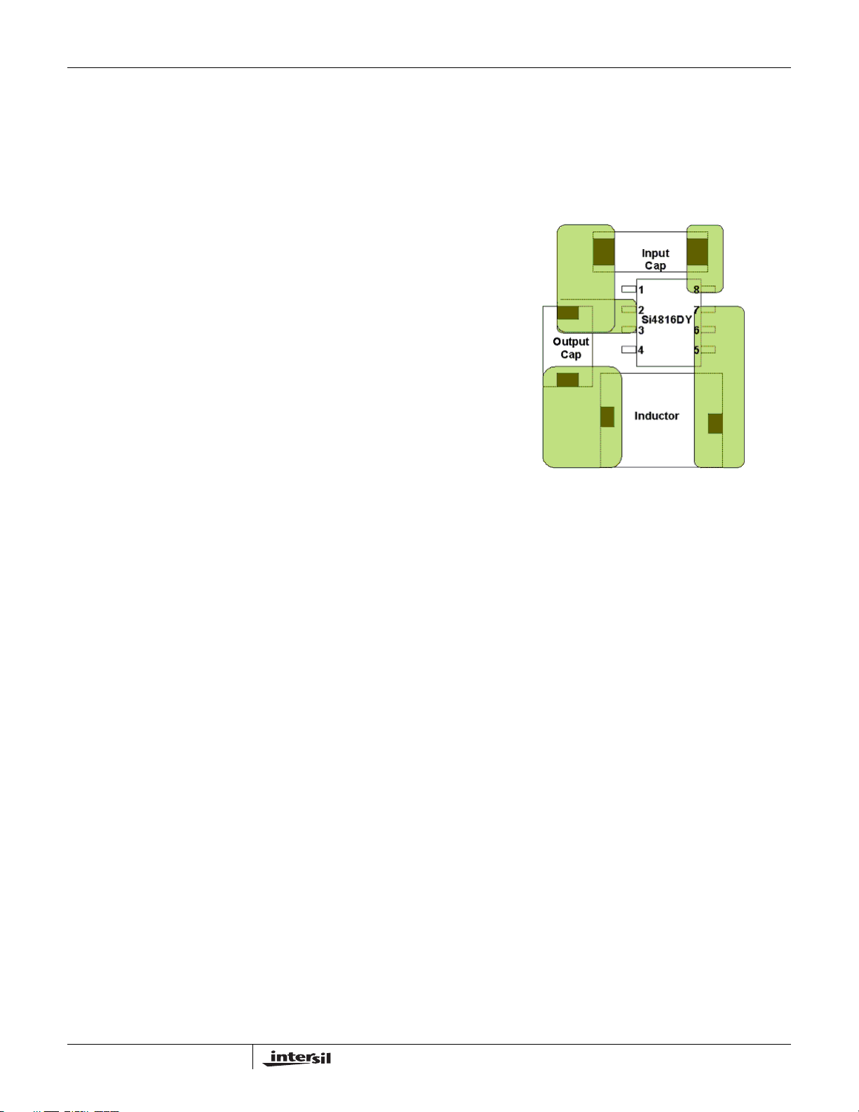
ISL6227
Copper Size for the Phase Node
Big coppers on both sides of the Phase node introduce
parasitic capacitance. The capacitance of PHASE should be
kept very low to minimize ringing. If ringing is excessive, it
could easily affect current sample information. It would be
best to limit the size of the PHASE node copper in strict
accordance with the current and thermal management of the
application.
Identify the Power and Signal Ground
The input and output capacitors of the converters, the source
terminals of the bottom switching MOSFET PGND1, and
PGND2, should be closely connected to the power ground.
The other components should connect to signal ground.
Signal and power ground are tied together at the negative
terminal of the output capacitors.
Decoupling Capacitor for Switching MOSFET
It is recommended that ceramic caps be used closely
connected to the drain side of the upper MOSFET, and the
source of the lower MOSFET. This capacitor reduces the
noise and the power loss of the MOSFET . Refer to Figure 43
for the power component placement.
-
-
V
o
+
+
FIGURE 43. A GOOD EXAMPLE POWER COMPONENT
REPLACEMENT. IT SHOWS THE NEGATIVE OF
INPUT AND OUTPUT CAP AND THE SOURCE OF
THE MOSFET ARE TIED AT ONE POINT.
V
V
IN
IN
- +
- +
L
o
L
o
26
FN9094.4
December 21, 2006
ISL6227
Quad Flat No-Lead Plastic Package (QFN)
Micro Lead Frame Plastic Package (MLFP)
2X
0.15
C
E1/2
E1
A2
A
A1
8
E2
7
9
CORNER
OPTION 4X
A1
A
E/2
9
/ /
9
(Ne-1)Xe
REF.
8
C
L
E
B
0.10 C
0.08
e
0.152XB
C
L1
C
L
10
A
6
INDEX
AREA
AREA
2X
2X
SEATING PLANE
(DATUM B)
(DATUM A)
INDEX
AREA
FOR ODD TERMINAL/SIDE FOR EVEN TERMINAL/SIDE
0.15
6
CC
4X
4X P
4X P
NX L
e
1
2
3
B
C
AC0.15
0
C
8
C
L
D
9
N
BOTTOM VIEW
D1
D1/2
N
TOP VIEW
SIDE VIEW
NX b
D2
D2
2
e
(Nd-1)Xe
REF.
NX b
5
L1
TERMINAL TIP
D/2
5
SECTION "C-C"
0.10 BAMC
7
NX k
N
1
2
3
L
10
A3
E2/2
L28.5x5
28 LEAD QUAD FLAT NO-LEAD PLASTIC PACKAGE
(COMPLIANT TO JEDEC MO-220VHHD-1 ISSUE I)
MILLIMETERS
SYMBOL
A 0.80 0.90 1.00 -
A1 - 0.02 0.05 -
A2 - 0.65 1.00 9
A3 0.20 REF 9
b 0.18 0.25 0.30 5,8
D 5.00 BSC -
D1 4.75 BSC 9
D2 2.95 3.10 3.25 7,8
E 5.00 BSC -
E1 4.75 BSC 9
E2 2.95 3.10 3.25 7,8
e 0.50 BSC -
k0.20 - - -
L 0.50 0.60 0.75 8
N282
Nd 7 3
Ne 7 3
P- -0.609
θ --129
NOTES:
1. Dimensioning and tolerancing conform to ASME Y14.5-1994.
2. N is the number of terminals.
3. Nd and Ne refer to the number of terminals on each D and E.
4. All dimensions are in millimeters. Angles are in degrees.
5. Dimension b applies to the metallized terminal and is measured
between 0.15mm and 0.30mm from the terminal tip.
6. The configuration of the pin #1 identifier is optional, but must be
located within the zone indicated. The pin #1 identifier may be
either a mold or mark feature.
7. Dimensions D2 and E2 are for the exposed pads which provide
improved electrical and thermal performance.
8. Nominal dimensions are provided to assist with PCB Land Pattern
Design efforts, see Intersil Technical Brief TB389.
9. Features and dimensions A2, A3, D1, E1, P & θ are present when
Anvil singulation method is used and not present for saw
singulation.
NOTESMIN NOMINAL MAX
Rev. 1 11/04
27
FN9094.4
December 21, 2006

ISL6227ISL6227
Shrink Small Outline Plastic Packages (SSOP)
Quarter Size Outline Plastic Packages (QSOP)
N
INDEX
AREA
123
-A-
E
-B-
SEATING PLANE
D
A
-C-
0.25(0.010) BM M
H
GAUGE
PLANE
0.25
0.010
h x 45°
L
α
e
B
0.17(0.007) C AM BS
M
A1
0.10(0.004)
NOTES:
1. Symbols are defined in the “MO Series Symbol List” in Section 2.2
of Publication Number 95.
2. Dimensioning and tolerancing per ANSI Y14.5M-1982.
3. Dimension “D” does not include mold flash, protrusions or gate
burrs. Mold flash, protrusion and gate burrs shall not exceed
0.15mm (0.006 inch) per side.
4. Dimension “E” does not include interlead flash or protrusions. Interlead flash and protrusions shall not exceed 0.25mm (0.010 inch)
per side.
5. The chamfer on the body is optional. If it is not present, a visual index feature must be located within the crosshatched area.
6. “L” is the length of terminal for soldering to a substrate.
7. “N” is the number of terminal positions.
8. Terminal numbers are shown for reference only.
9. Dimension “B” does not include dambar protrusion. Allowable dambar protrusion shall be 0.10mm (0.004 inch) total in excess of “B”
dimension at maximum material condition.
10. Controlling dimension: INCHES. Converted millimeter dimensions
are not necessarily exact.
A2
C
M28.15
28 LEAD SHRINK SMALL OUTLINE PLASTIC PACKAGE
(0.150” WIDE BODY)
INCHES MILLIMETERS
SYMBOL
A 0.053 0.069 1.35 1.75 A1 0.004 0.010 0.10 0.25 A2 - 0.061 - 1.54 -
B 0.008 0.012 0.20 0.30 9
C 0.007 0.010 0.18 0.25 D 0.386 0.394 9.81 10.00 3
E 0.150 0.157 3.81 3.98 4
e 0.025 BSC 0.635 BSC -
H 0.228 0.244 5.80 6.19 -
h 0.0099 0.0196 0.26 0.49 5
L 0.016 0.050 0.41 1.27 6
N28 287
α
0° 8° 0° 8° -
NOTESMIN MAX MIN MAX
Rev. 1 6/04
All Intersil U.S. products are manufactured, assembled and tested utilizing ISO9000 quality systems.
Intersil Corporation’s quality certifications can be viewed at www.intersil.com/design/quality
Intersil products are sold by description only. Intersil Corporation reserves the right to make changes in circuit design, software and/or specifications at any time without
notice. Accordingly, the reader is cautioned to verify that data sheets are current before placing orders. Information furnished by Intersil is believed to be accurate and
reliable. However, no responsibility is assumed by Intersil or its subsidiaries for its use; nor for any infringements of patents or other rights of third parties which may result
from its use. No license is granted by implicat ion or oth erwise u nde r any p a tent or p at ent r ights of Intersil or its subsidiaries.
For information regarding Intersil Corporation and its products, see www.intersil.com
28
FN9094.4
December 21, 2006
 Loading...