

查询ISL6226EVAL1供应商
®
ISL6226
Data Sheet August 2002
Advanced PWM and Linear Power
Controller for Portable Applications
The ISL6226 provides power control and protection for two
user selected output voltages required in high-performance
notebook PC applications. The IC integrates a fixed,
selectable frequency pulse-width-modulation (PWM)
controller and a 3A LDO linear regulator controller with
monitoring and protection circuitry in a single 24 lead SSOP
package.
The PWM controller regulates the battery input voltage to a
user selected output voltage. Synchronous converter and
hysteretic operation at light loads contribute to a high
efficiency over a wide range of input voltage and load
variation. Efficiency can be further enhanced by using the
lower MOSFET’s r
DS(ON)
voltage feed-forward ramp modulation, current-mode control,
and internal feed-back compensation provide fast and stable
handling of input voltage load transients encountered in
advanced portable computer chip sets.
as the current sense element. Input
FN9078.1
Features
• Provides Two Regulated Voltages
- Linear Regulator, User Selected, Current Limited
- High Efficiency PWM Over Wide Line and Load Range
- Synchronous Buck Converter on PWM Output
- Hysteretic Operation at Light Load
• Dual Mode Operation:
- Directly From Battery Input, V
VCC of 5V
• PWM Output Adjustable From 0.9V to 0.93*V
• Low Drop-Out (LDO) Linear Regulator Operates from
Vout+0.5V to 24V
• LDO Output Adjustable
- From 0.8V to 3.8V at 0A to 3A for NPN Transistor
- From 0.8V to 3.0V at 0A to 3A for N-MOSFET
• 300/600kHz Switching Frequency Selectable
, of 5.6V to 24V or from
IN
IN
The internal linear regulator controller provides a user
selected high current output from an unregulated input with
user selected current limit.
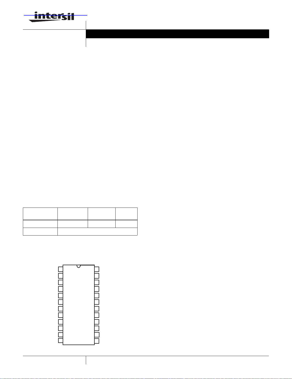
Ordering Information
PART
NUMBER
ISL6226CA -10 to 85 24 Ld SSOP M24.15
ISL6226EVAL1 Evaluation Board
TEMP. RANGE
o
(
C) PACKAGE PKG. NO.
Pinout
ISL6226 (SSOP)
TOP VIEW
24
23
22
21
20
19
18
17
16
15
14
VOUT
VSEN
FPWM
PGOODP
ISEN
BOOT
UGATE
PHASE
SSPWM
PVCC
LGATE
PGND
VIN
PGOODL
PWMEN
OCSET
LINEN
VCC
LINDR
LINCS1
LINCS2
SSLIN
LINVS
GND
1
2
3
4
5
6
7
8
9
10
11
12 13
• Forced PWM Mode Control Option
• No Current-Sense Resistor Required on PWM Output
- Uses MOSFET’s r
DS(ON)
- Optional Current-Sense Resistor for More Precision
• Separate Soft-Start For Both PWM and LDO
• Separate Enable Pins for both PWM and LDO for
Advanced Configuration and Power Interface (ACPI)
Compatibility
• Input Under voltage Lock-Out (UVLO) Protection
• Excellent Dynamic Response
- Input Voltage Feed-Forward and Current-Mode Control
• Monitors Output Voltages and Provides PGOOD Status
• Thermal Shut-Down Protection
Applications
•
Mobile PCs
• Hand-Held Portable Instruments
• Other Devices and Appliances With up to 24V Input
Related Literature
• AN1013
1
CAUTION: These devices are sensitive to electrostatic discharge; follow proper IC Handling Procedures.
1-888-INTERSIL or 321-724-7143
| Intersil (and design) is a registered trademark of Intersil Americas Inc.
Copyright © Intersil Americas Inc. 2002. All Rights Reserved
ISL6226
Absolute Maximum Ratings Thermal Information
Bias Voltage, Vcc. . .. . . . . . . . . . . . . . . . . . . . . . . . . . . . . . . -0.3V to + 7V
Input Voltage, VIN . . . . . . . . . . . . . . . . . . . . . . . . . . . . . . . . . . . . . +30.0V
Phase and Isen Pins . . . . . . . . . . . . . . . . . . . . . GND-0.3V to +30.0V
Boot and Ugate Pins . . . . . . . . . . . . . . . . . . . . . . . . . . . . . . . . . . + 35.0V
BOOT with respect to PHASE . . . . . . . . . . . . . . . . . . . . . . . . . .+ 7.0V
Imax for LINDR Pin. . . . . . . . . . . . . . . . . . . . . . . . . . . . . . . . . . . . .70mA
All other pins . . . . . . . . . . . . . . . . . . . . . . . . . . . . . GND -0.3V to 7V
ESD Classification . . . . . . . . . . . . . . . . . . . . . . . . . . . . . . . . . Class 1
Recommended Operating Conditions
Bias Voltage, Vcc. . . . . . . . . . . . . . . . . . . . . . . . . . . . . . . .+ %
Input Voltage, VIN . . . . . . . . . . . . . . . . . . . . . . . . . . . +5.6V to +24.0V
Ambient Temperature Range. . . . . . . . . . . . . . . . . . . -10
Junction Temperature Range. . . . . . . . . . . . . . . . . . -10
CAUTION: Stresses above those listed in “Absolute Maximum Ratings” may cause permanent damage to the device. This is a stress only rating and operation of the
device at these or any other conditions above those indicated in the operational sections of this specification is not implied.
NOTE:
1. θ
JA is measured with the component mounted on a high effective thermal conductivity test board in free air. See Tech Brief TB379 for details.
5.0V 5±
o
C to 85oC
o
C to 125oC
Thermal Resistance (Typical, Note 1) θ
SSOP Package . . . . . . . . . . . . . . . . . . . . . . . . . . . . 90
Maximum Junction Temperature (Plastic Package) . . 150
Maximum Storage Temperature Range. . . . . . . . . . -65
(oC/W)
JA
o
C
o
C to 150oC
Maximum Lead Temperature (Soldering 10s) . . . . . . . . . . . . .300
(SSOP - Lead Tips Only)
o
C
Electrical Specifications Operating Conditions: Vcc = 5V, T
= -10oC to 85oC, Unless Otherwise Noted.
A
PARAMETER SYMBOL TEST CONDITIONS MIN TYP MAX UNITS
VCC SUPPLY
Bias Current I
Bias Current I
CC
CC
LGATE, UGATE Open, VSEN forced above
regulation point (Fs = 300K Hz)
LGATE, UGATE Open, VSEN forced above
- 1100 - µA
- 1100 - µA
regulation point (Fs = 600K Hz)
Shut-down Current I
CCSN
-525µA
VCC UVLO
Rising Vcc Threshold 4.30 - 4.65 V
Falling Vcc Threshold 4.1 - 4.45 V
Vcc Hysterises 30 500 mV
VIN
Input Voltage Pin Current (Sink) I
Input Voltage Pin Current (Source) I
Shut-down Current I
VIN
VIN
VIN
VIN pin connected to the input voltage
10 20 30 µA
source
VIN pin connected to ground -7 -12 -17 µA
--1µA
OSCILLATOR
PWM Oscillator Frequency F
PWM Oscillator Frequency F
Ramp Amplitude, pk-pk V
Ramp Amplitude, pk-pk V
Ramp Offset V
ROFF
VIN=3.5V -- 24V 255 300 345 kHz
c1
V
c2
R1
R2
≤0.5V 510 600 690 kHz
IN
VIN= 16V - 2 - V
V
≤5V - 1.25 - V
IN
-0.5- V
PWM CONTROLLER
REFERENCE AND SOFT START
PWM Internal Reference Voltage V
PWM Soft-Start Threshold V
REF
SOFT
-0.9- V
-1.5- V
Reference Voltage Accuracy -2.0 - +2.0 %
2
ISL6226
PARAMETER SYMBOL TEST CONDITIONS MIN TYP MAX UNITS
Soft-Start Current During Start-up I
SOFT
PWM CONVERTER
Load Regulation 0.0mA < I
VSEN pin bias current I
VOUT pin input impedance I
Under-Voltage Shut-Down Level V
VSEN
VOUT
UV1
Fraction of the set point; ~3µs noise filter 70 - 76 %
< 5.0A; 5.0V < VIN < 24.0V -2.0 - +2.0 %
VOUT1
Under Voltage Delay UV_DLY 3 - 5.5 uS
Over-Voltage Protection V
OVP1
Fraction of the set point; ~1µs noise filter 113.5 - 118 %
Over Voltage Delay OVP_DLY 0.5 - 2.7 uS
PWM CONTROLLER GATE DRIVER
Upper Drive Pull-Up Resistance R
Upper Drive Pull-Down Resistance R
Lower Drive Pull-Up Resistance R
Lower Drive Pull-Down Resistance R
2UGPUP
2UGPDN
2LGPUP
2LGPDN
POWER GOOD AND CONTROL FUNCTIONS
Power Good Lower Threshold V
Power Good Higher Threshold V
PGOOD Leakage Current I
PG-
PG+
PGLKG
PGOOD Voltage Low I
Fraction of the set point; ~3µs noise filter -13.5 - -7.5 %
Fraction of the set point; ~3µs noise filter 7.4 - 13.5 %
V
PGOOD
= 5.5V - - 1 µA
PULLUP
= -4mA - - 0.5 V
EN- Low (Off) --0.8V
EN - High (On) 2.0 - - V
FCCM -Hysteretic Operation Enabled -Vcc/2- V
LOW DROP OUT CONTROLLER FUNTIONS
Linear Input Voltage Vin No External Passive Device - Vcc - V
Linear Input Voltage Vin With External Passive Device Device Rating
Linear Output Voltage LDOout No External Passive Device 0.8 - 4.5 V
Output Drive Current for NPN I(DRV) out 50 - - mA
OverCurrent Feedback Voltage V(CS) 100 mV
Under-Voltage Shut-Down Level V
Under-Voltage Delay UV
UV
Fraction of the set point; ~3µs noise filter 71 74 77 %
DLY
REFERENCE AND SOFT START
LDO Internal Reference Voltage V
LDO Soft-Start Threshold V
REF
SOFT
Reference Voltage Accuracy -2.0 - +2.0 %
Soft-Start Current During Start-up I
SOFT
POWER GOOD AND CONTROL FUNTIONS
Power Good Lower Threshold V
Power Good Higher Threshold V
PG-
PG+
Vo<V
Vo>V
REF
REF
PGOOD Leakage Current IPGLKG VPULLUP = 5.5V - - 1.0 uA
PGOOD Voltage Low VPGOOD IPGOOD = -4mA, VCC = 4.75V - - 0.5 V
LINEN-Low (OFF) --0.8V
-5- µA
-80- nA
135 150 198 kOhm
6.2 8.5 13.5 Ω
2.5 3.0 4.7 Ω
6.2 8.5 13.4 Ω
1.3 1.6 2.7 Ω
5.5 - 8 uS
-0.8- V
1.5 V
-5- µA
-15.5 -12 -9 %
10.5 13.5 16.5 %
3
ISL6226
PARAMETER SYMBOL TEST CONDITIONS MIN TYP MAX UNITS
LINEN-High (ON) 2.0 - - V
Input Bias Current LINCS1 and LINCS2 Ibias1 Vlincs = 0.8 V - -80 - nA
Input Bias Current LINVS Ibias2 Vlinvs = 0.8 V - -80 - nA
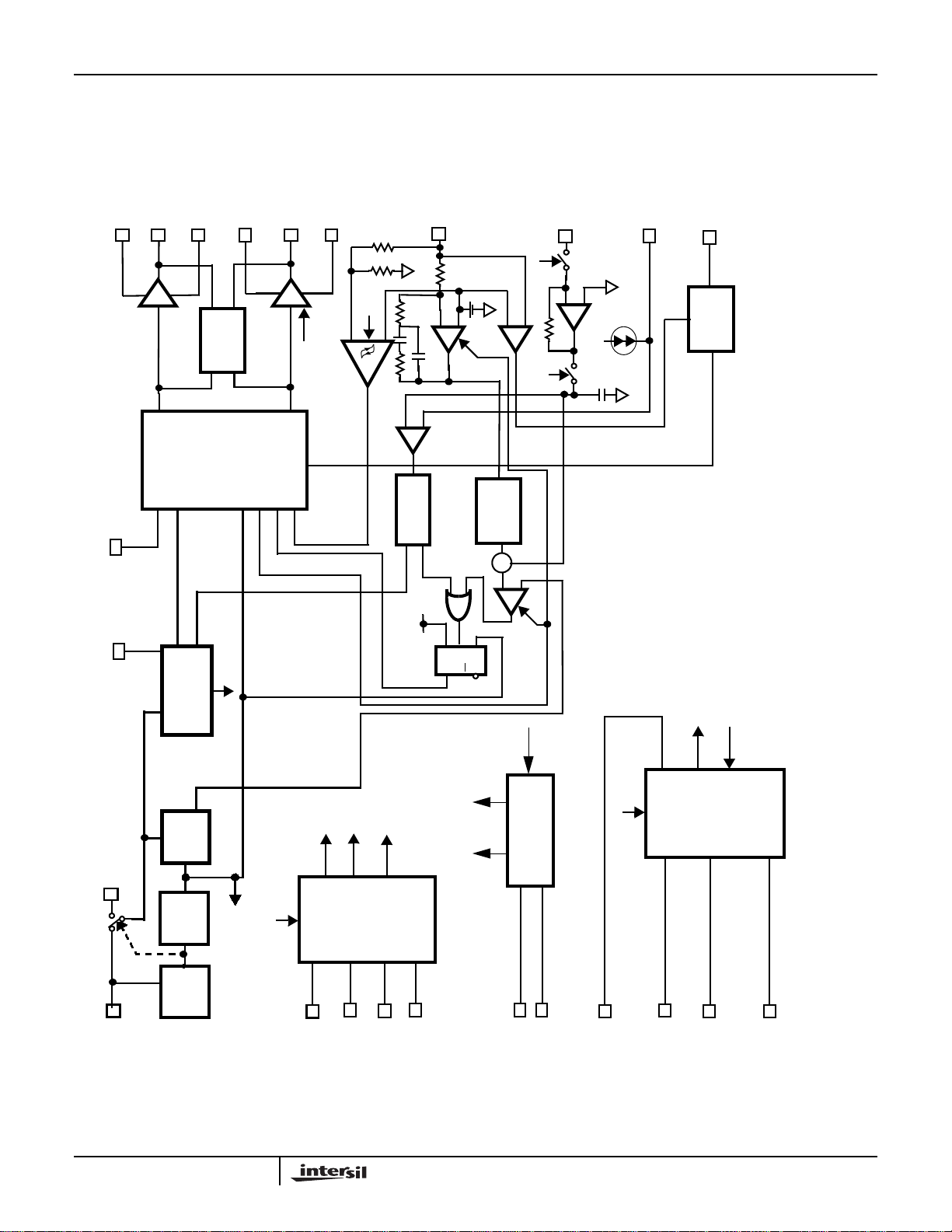
Functional Pin Descriptions
VIN (Pin 1)
Provides battery voltage to the oscillator for feed-forward
rejection of the input voltage variation. Also, this pin programs
frequency of the internal clock and gain of the ramp generator.
PGOODL (Pin 2)
PGOODL is an open drain output used to indicate the status of
the LDO output voltages. This pin is pulled low when the output
voltage is not within of its respective nominal voltage or over
120mV between pin 8 and 9.
PWMEN (Pin 3)
This pin provides enable/disable function the PWM output.
The output is enabled when this pin is high. The PWM output
is held off when this pin is pulled to ground. Intersil
recommends to use hysteresis mode when input voltage
higher than 18V and output voltage is 1.25V or less.
OCSET (Pin 4)
A resistor on this pin to ground sets the over current
threshold for the PWM controller.
LINEN (Pin 5)
This pin provides enable/disable function and soft-start for
the LDO. The output is enabled when this pin is high. The
LDO is held off when this pin is pulled to ground.
VCC (Pin 6)
Input power for the controller and the upper MOSFET gate
drive. The IC starts to operate when the voltage on this pin
exceeds 4.3V and stops operating when the voltage on this
pin drops below approximately 4.45V.
LINDR (Pin 7)
Current output to drive the NPN transistor.
LINCS1 (Pin 8)
High side of current sense resistor.
LINCS2 (Pin 9)
Low side of current sense resistor. Current limit for the linear
regulator is initiated when the voltage difference between
LINCS1 and LINCS2 is 120mV.
SSLIN (Pin 10)
This pin provides soft start of the LDO controller. When the EN
pin is pulled high, the voltage on the capacitor connected to
the soft start pin is rising linearly due to the 5 pull-up
current. The output voltage follows the voltage on the
µA
capacitor till it reaches the value of 0.8V. At this moment the
output voltage starts to regulate and soft start continues to rise
to 1.5V. At this time, the soft start is complete and the
PGOODL will be high to indicate the output voltage within its
respective nominal voltage. The further rise of soft start
capacitor does not affect the output voltage. The soft-start
time can be obtained from the following equation.
Tsslin
1.5VxCss
----------------------------=
5µA
LINVS (Pin 11)
Voltage regulation point (0.8V) for the linear output.
GND (Pin 12)
Signal ground for the IC. All voltage levels are measured
with respect to this pin.
PGND (Pin 13)
This is the lower MOSFET gate drive return connection for
PWM converter. Tie the lower MOSFET source directly to
this pin.
LGATE (Pin 14)
This pin provides the gate drive for the lower MOSFET.
Connect the lower MOSFET gate to this pin.
PVCC (Pin 15)
This pin powers the lower MOSFET gate driver.
SSPWM (Pin 16)
This pin provides soft start of the PWM controller. This pin has
the same function as SSLIN pin. When the EN pin is pulled
high, the voltage on the capacitor connected to the soft start
pin is rising linearly due to the 5
output voltage follows the voltage on the capacitor till it
reaches the value of 0.9V. At this moment the output voltage
starts to regulate and soft start continues to rise to 1.5V. At this
time, the soft start is complete and the PGOODPWM will be
high to indicate the output voltage within its respective
nominal voltage. The further rise of soft start capacitor does
not affect the output voltage. The soft-start time can be
obtained from the following equitation.
Tsspwm
1.5VxCss
----------------------------=
5µA
pull-up current. The
µA
PHASE (Pin17)
The phase node is the junctions of the upper MOSFET
source, output filter inductor, and lower MOSFET drain.
Connect the PHASE pin directly to the PWM converter’s lower
MOSFET drain.
4

ISL6226
UGATE (Pin18)
This pin provides the gate drive for the upper MOSFET.
Connect UGATE pin to the PWM converter’s upper
MOSFET gate.
BOOT (Pin 19)
Power is supplied to the upper MOSFET driver of the PWM
converter via the BOOT pin. Connect this pin to the junction
the bootstrap capacitor with the cathode of the bootstrap
diode. The anode of the bootstrap diode is connected to pin
6, VCC.
ISEN (Pin 20)
This pin is used to monitor the voltage drop across the lower
MOSFET for current feedback control. For more precise
current detection, this input can be connected to optional
current sense resistors placed in series with the source of
the lower MOSFET.
PGOODP (Pin 21)
PGOODP is an open drain output used to indicate the status
of the PWM converter’s output voltages. This pin is pulled
low when the output is not within of their respective nominal
voltage.
FPWM (Pin 22)
This pin when pulled to VCC restrains hysterectic operation
in light loads.
VSEN (Pin 23)
This pin is connected to the PWM voltage divider to provide
the voltage feedback signal for the PWM controller. The
PGOODP, overvoltage protection (OVP) and undervoltage
shutdown circuits use this signal to determine output voltage
status and/or to initiate undervoltage shut down.
VOUT (Pin 24)
The output voltage is sensed on this pin to provide feedback
during the PWM to Hysteretic mode transition.
5
ISL6226
BOOT
FPWM
GND
UGATE
HGDR1
HI
FPWM
PHASE
SHUTOFF
PVCC
GATE
CONTROL
GATE LOGIC
POR
DEADT
PWM/HYST
LGATE
LGDR
LO
PWM ON
PGND
OVP
HYST ON
COMP
-
+
FFBK
CLAMP
S
-
+
ISEN
LGATE
-
+
R1=20K
LGATE1
VSEN
+
-
CLK1
-
+
HYST COMP1
OC COMP1
-
+
OC LOGIC1
VCC
PWM
LATCH 1
EA
-
+
D
Q
MODE CHANGE
REF
VOLTAGE
<
R
Q
OCSET
VOUT
PWM/HYS
LOGIC
POWER-ON
RESET (POR)
VSEN
LINDR
POR
LINCS1
OUTPUT
MONITOR
RAMP
VCC
VIN
CLK
CLK
POR
FSET
PWMEN
SDWN
REFERENCE
LINEN
REF
AND
SOFT START
SSPWM
OVP UVO
SSLIN
VOLTAGE
PGOODP
PGOODL
SDWN
LINEAR
CONTROLLER
LINCS2
REF
LINVS
FIGURE 1. FUNCTIONAL BLOCK DIAGRAM
6

ISL6226
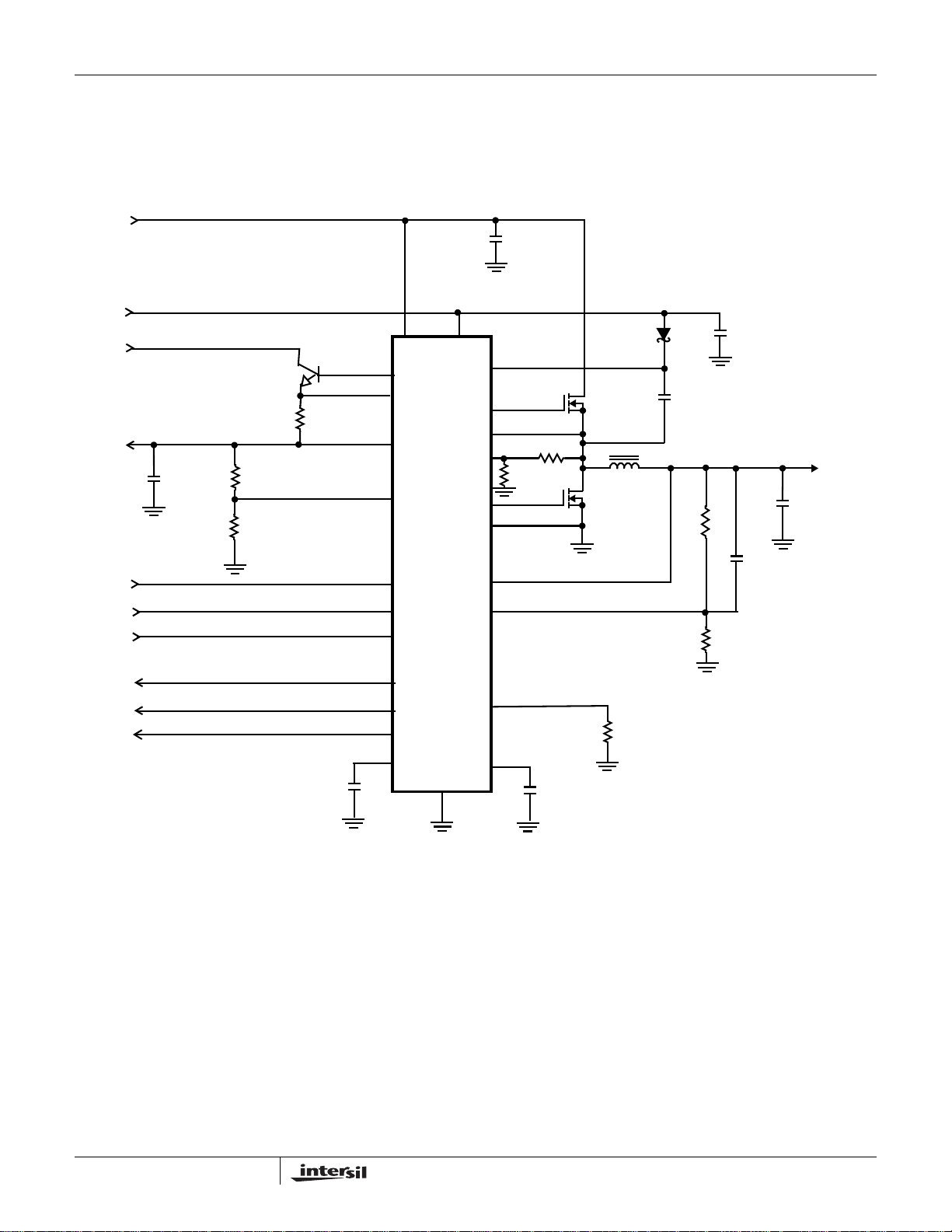
+5.6-24 V
GND
0A to 50mA
IN
5V
Vout = 0.8V - 4.5V
C5
10µF
R2
R3
+
R1
LINDR
LINCS1
LINCS2
LINVS
LINEN
PWMEN
FPWM
VIN
1
7
8
9
ISL6226
11
5
3
22
VCC
6
C2, 3
2x10µF
D1
BAT54WT1
BOOT
19
UGATE
18
PHASE
17
20
14
13
24
23
ISEN
200
LGATE
PGND
VOUT
VSEN
R4
1K
Q2
1/2 FDS6982S
L2
6.4µH
Q3
1/2 FDS6982S
C5
0.15µF
R7
C4
1µF
Vout = 0.9V - 0.93*V
R5
C8
+
(3A)
C6
1x330µF
IN
PVCC
15
PGOODL
PGOODP
C10
SSLIN
2
21
10
12
GND
4
16
OCSET
R8
SSPWM
C11
FIGURE 2. 0A to 50mA OUTPUT CURRENT LDO AND SYNCHORNOUS BUCK CONVERTER (Fs=300KHz)
7

ISL6226
+5.6-24 V
3A
IN
5V
LINEAR INPUT
Vout = 0.8V - 3.0V
+
C5
330µF
R2
R3
Q1
R1
LINDR
LINCS1
LINCS2
LINVS
LINEN
PWMEN
FPWM
7
8
9
11
5
3
22
VIN
1
ISL6226
VCC
6
C2, 3
2x10µF
D1
BAT54WT1
BOOT
19
UGATE
18
PHASE
17
20
14
13
24
23
ISEN
200
PGND
VOUT
VSEN
R4
1K
LGATE
Q2
1/2 FDS6982S
L2
6.4µH
Q3
1/2 FDS6982S
C5
0.15µF
R7
C4
1µF
Vout = 0.9V - 0.93*V
R5
C8
+
IN
(3A)
C6
1x330µF
PVCC
15
PGOODL
PGOODP
C10
Figure 3. LDO WITH EXTERNAL N-MOSFET AND SYNCHORNOUS BUCK CONVERTER (Fs = 300KHz)
SSLIN
2
21
10
12
GND
4
16
OCSET
R8
SSPWM
C11
8
ISL6226
+5.6-24 V
3A
IN
5V
LINEAR INPUT
Vout = 0.8V - 3.8V
+
C5
330µF
R2
R3
Q1
R1
LINDR
LINCS1
LINCS2
LINVS
LINEN
PWMEN
FPWM
8
9
11
3
1
7
5
22
VIN
ISL6226
VCC
6
C2, 3
2x10µF
D1
BAT54WT1
BOOT
19
UGATE
18
PHASE
17
20
14
13
24
23
ISEN
200
PGND
VOUT
VSEN
R4
1K
LGATE
Q2
1/2 FDS6982S
L2
6.4µH
Q3
1/2 FDS6982S
C5
0.15µF
R7
C4
1µF
Vout = 0.9V - 0.93*V
R5
C8
+
(3A)
C6
1x330µF
IN
PVCC
PGOODL
PGOODP
SSLIN
C10
15
OCSET
12
GND
4
16
R8
SSPWM
C11
2
21
10
FIGURE 4. LDO with External NPN and Synchornous Buck Converter (Fs = 300KHz)
9

ISL6226
5V
LINEAR INPUT
Vout = 0.8V - 3.8V
3A
+
C5
330µF
R2
R3
Q1
R1
PWMEN
PGOODL
PGOODP
C10
150K
LINDR
LINCS1
LINCS2
LINVS
LINEN
FPWM
PVCC
SSLIN
R6
VIN
1
7
8
9
11
5
3
22
15
2
21
10
ISL6226
12
GND
VCC
6
19
18
17
20
14
13
24
23
4
16
C2
2 x10µF
BOOT
UGATE
PHASE
ISEN
200
LGATE
PGND
VOUT
VSEN
OCSET
SSPWM
R4
1K
C11
BAT54WT1
Q2
1/2 FDS6982S
L2
6.4µH
Q3
1/2 FDS6982S
R8
D1
C5
0.15µF
R5
R7
Vout = 0.9V - 0.93*V
+
C6
1x330µF
C8
IN
(2A)
FIGURE 5. APPLICATION CIRCUIT FOR TWO STEP 300 kHz CONVERSION (MODE 2)
NOTE: Q1 can be either N-MOSFET, NPN or not use for 50 mA
10

5V
LINEAR INPUT
Vout = 0.8V - 3.8V
3A
+
C5
330µF
R2
R3
Q1
R1
LINDR
LINCS1
LINCS2
LINVS
1
7
8
9
11
VIN
ISL6226
ISL6226
VCC
6
BOOT
19
UGATE
18
PHASE
17
ISEN
20
14
PGND
13
C2
2 x10µF
200
LGATE
R4
1K
BAT54WT1
Q2
1/2 FDS6982S
L2
6.4µH
Q3
1/2 FDS6982S
D1
C5
0.15µF
R5
Vout = 0.9V - 0.93*V
(2A)
+
C6
1x330µF
IN
LINEN
PWMEN
FPWM
PVCC
PGOODL
PGOODP
SSLIN
C10
5
3
22
15
2
21
10
FIGURE 6. APPLICATION CIRCUIT FOR TWO STEP 600 kHz CONVERSION (MODE 3)
NOTE: Q1 can be either N-MOSFET, NPN or not used for 50
mA
12
GND
VOUT
24
VSEN
23
R7
OCSET
4
16
SSPWM
C11
R8
C8
11

ISL6226
Description Of Operation
The ISL6226 is a single channel PWM controller and linear
regulator controller intended for chipset, DRAM, audio or
other low voltage power needs of modern notebook and subnotebook PCs. The IC integrates control circuits for a single
synchronous buck converter whose output voltage is set in
the range of 0.9V to 0.93*Vin by an external resistive divider
and a linear regulator controller which drives an external
NMOSFET or NPN pass transistor whose output is set in the
range of 0.8V to 3.8V by an external resistor divider. The
synchronous buck converter can be operated in several
modes to optimize the application. The 300kHz frequency
operation is recommended when powered from the battery,
which voltage varies from 5.6V to 24V. In this case the V
pin is connected to the battery terminal and the ramp
generator gain is dynamically adjusted according to the input
voltage.
The IC also can be optimized for a two stage power
conversion configuration where the output voltage is derived
from a 5V input in lieu of the raw battery. Two operating
frequencies of 300kHz or 600kHz are available in this mode.
If 300kHz operation is desired while operating from the 5V
system bus, the V
pin should be connected to ground via a
IN
150K ohm resistor. The ramp generator gain is corrected for
the lower input voltage.
When powered from the system 5V rail, the converter can be
configured to operate on increased frequency of 600kHz to
minimize the output filter components. In this case, the V
pin is connected to the ground. Table 1 summarizes the
various modes of operation.
Figure 7 below shows plots of
the ramp speed compensation.
Table 1. Configuration for Modes of Operation
Operation
One stage 300kHz V
Two stage 300kHz 150K-GND 1V<V1<2V
Two stage 600kHz GND V1<0.5V
Pin 1
connection
IN
Pin 1 potential
V1>5.6V
IN
IN
Current Sensing and Current Limit Protection
The PWM converter uses the lower MOSFET on-state
resistance, r
technique eliminates the need for a current sense resistor
and the associated power losses. If more accurate current
protection is desired, current sense resistors may be used in
series with the lower MOSFETs’ source.
A current proportional signal is used to provide average
current mode control and over-current protection. The gain
in the current sense circuit is set by the resistor connected
from ISEN pin to the switching node of buck converter. The
value of this resistor can be estimated by the following
expression:
where Iomax is the maximum inductor current. The value of
Risen should be specified for the expected maximum
MOSFET operating temperature.
The resulting current out of the ISEN pin through Risen, is
used for current feedback and current limit protection. An
over-current protection threshold is set by an external
resistor connected from OCSET (pin 4) to ground. The value
of this resistor can be obtained from the following
expression:
where Ioc is the value of over current. This is compared
with an internal current limit threshold. When a sampled
value of the output current is determined to be above the
current limit threshold, the PWM drive is terminated and a
counter is initiated. This limits the inductor current build-up
and essentially switches the converter into current-limit
mode. If an overcurrent is detected between 26µs to 53µs
later, an overcurrent shutdown is initiated. If during the
26µs to 53µs period, an overcurrent is not detected, the
counter is reset and sampling continues as normal.
, as the current-sensing element. This
DS(ON)
Risen
Rocset
Iomax Rdson•
------------------------------------------- 100–=
75µA
9.6 Ri s en 100–()•
----------------------------------------------------=
Ioc Rdson•
300kHz CLOCK
600kHz CLOCK
Vin
---------
t
---
2
T
Vin
---------
t
---
4
T
Vin
---------
8
Figure 7. Ramp Speed Compensation Vo=2.5V
12
This current limit scheme has proven to be very robust in
applications like portable computers where fast inductor
current build-up is common due to a large difference
between input and output voltages and a low value of the
t
---
T
inductor.
Light-Load (Hysteretic) Operation
In the light-load (hysteretic) mode the output voltage is
regulated by the hysteretic comparator which regulates the
output voltage by maintaining the output voltage ripple as
shown in Figure 8. In Hysteretic mode, the inductor current
flows only when the output voltage reaches the lower limit of
the hysteretic comparator and turns off at the upper limit.
Hysteretic mode saves converter energy at light loads by
supplying energy only at the time when the output voltage

C
ISL6226
requires it. This mode conserves energy by reducing the
power dissipation associated with continuous switching.
During the time between inductor current pulses, both the
upper and lower MOSFETs are turned off. This is referred to
as ‘diode emulation mode’ because the lower MOSFET
performs the function of a diode. This diode emulation mode
prevents the output capacitor from discharging through the
lower MOSFET when the upper MOSFET is not conducting.
NOTE: the FPWM operation can intentionally be forced by tying pin
22, FPWM, to Vcc.
Operation-Mode Control
The mode-control circuit changes the converter’s mode of
operation based on the voltage polarity of the phase node
when the lower MOSFET is conducting and just before the
upper MOSFET turns on. For continuous inductor current,
the phase node is negative when the lower MOSFET is
conducting and the converter operates in fixed-frequency
PWM mode as shown in Figure 9. When the load current
decreases to the point where the inductor current flows
through the lower MOSFET in the ‘reverse’ direction, the
phase node becomes positive, and the mode is changed to
hysteretic.
A phase comparator handles the timing of the phase node
voltage sensing. A low level on the phase comparator output
indicates a negative phase voltage during the conduction
time of the lower MOSFET. A high level on the phase
comparator output indicates a positive phase voltage.
When the phase node is positive (phase comparator high),
at the end of the lower MOSFET conduction time, for eight
consecutive clock cycles, the mode is changed to hysteretic
as shown in Figure 9. The dashed lines indicate when the
phase node goes positive and the phase comparator output
goes high. The solid vertical lines at 1,2,...8 indicate the
sampling time, of the phase comparator, to determine the
polarity (sign) of the phase node. At the transition between
PWM and hysteretic mode both the upper and lower
MOSFETs are turned off. The phase node will ‘ring’ based
on the output inductor and the parasitic capacitance on the
phase node and settle out at the value of the output voltage.
PWM on the next clock cycle. This insures the full power
required by the increase in output current.
Gate Control Logic
The gate control logic translates generated PWM control
signals into the MOSFET gate drive signals providing
necessary amplification, level shifting and shoot-through
protection. Also, it has functions that help optimize the IC
performance over a wide range of operational conditions.
Since MOSFET switching time can vary dramatically from
type to type and with the input voltage, the gate control logic
provides adaptive dead time by monitoring the gate-tosource voltages of both upper and lower MOSFETs. The
lower MOSFET is not turned on until the gate-to-source
voltage of the upper MOSFET has decreased to less than
approximately 1 volt. Similarly, the upper MOSFET is not
turned on until the gate-to-source voltage of the lower
MOSFET has decreased to less than approximately 1 volt.
This allows a wide variety of upper and lower MOSFETs to
be used without a concern for simultaneous conduction, or
shoot-through.
VOUT
I
L
PHASE
COMP
MODE
OF
OPERATION
I
L
1 2 3 4 5 6 7 8
PWM
FIGURE 8. REGULATION IN HYSTERETIC MODE
HYSTERETIC
t
t
t
t
t
The mode change from hysteretic to PWM can be caused by
one of two events. One event is the same mechanism that
causes a PWM to hysteretic transition. But instead of looking
for eight consecutive positive occurrences on the phase
node, it is looking for eight consecutive negative
occurrences on the phase node. The operation mode will be
changed from hysteretic to PWM when these eight
consecutive pulses occur. This transition technique prevents
jitter of the operation mode at load levels close to boundary.
The other mechanism for changing from hysteretic to PWM
is due to a sudden increase in the output current. This step
load causes an instantaneous decrease in the output voltage
due to the voltage drop on the output capacitor ESR and
ESL. If the decrease causes the output voltage to drop
below the hysteretic regulation level, the mode is changed to
13
PHASE
NODE
PHASE
COMP
MODE
OF
OPERATION
1 2 3 4
PWM
FIGURE 9. MODE CONTROL WAVEFORMS
5 6
7 8
HYSTERETI
t
t
t

ISL6226
Feedback Loop Compensation
To reduce the number of external components and remove
the burden of determining compensation components from a
system designer, PWM controller has internally
compensated error amplifiers. To make internal
compensation possible several design measures where
taken.
First, the ramp signal applied to the PWM comparator is
proportional to the input voltage provided via the VIN pin as
shown in Figure 7. Second, the load current proportional
signal is derived from the voltage drop across the lower
MOSFET during on time of lower MOSFET. This signal is
added to the amplifier error signal on the comparator input.
This effectively creates an internal current control loop.
Because of current loop, a compensation network with one
zero and two poles is usually sufficient. One pole is place at
origin which has high DC gain. The zero is place around
9kHz, and another pole is around 137kHz. The zero-pole
pair causes a flat gain region at frequencies in between the
zero and the pole. This region is also make the phase bump
or reduce phase shift. The amount of phase shift reduction
depends on how wide the region of flat gain and has
maximum value of 90
o
.
Low Drop Out Linear Regulator
The linear has separate Enable, Pgood and Soft Start pins
from the PWM. The linear also has over current and under
voltage protection features.
The over current protection will shut down the LDO controller
when the voltage between pin 8 and 9 is more 100mV. The
LDO controller will automatic restart again when the voltage
is less than 100mV. Intersil recommend to use this feature to
protect the ISL6226 IC otherwise the IC will damage when
over current happen.
The under voltage protection will start when the output
voltage is 26% lower than the nominal output voltage.
The ISL6226 has an internal P-channel MOSFET pass
transistor. This provides several advantages over PNP pass
transistor. PNP regulator waste considerable amounts of
current in dropout when the pass transistor saturates. The Pchannel MOSFET requires no base drive current which
reduces quiescent current.
Output Voltage Calculation
Figure 10 describe the output voltage which relative to the
bias voltage. Due to the over current protection circuitry
works properly, the internal P-channel MOSFET has an
approximate 0.5V drop cross it. Therefore, the maximum
voltage at LINDR pin will be.
VLINDR VCC 0.5V–=
The maximum output voltage equals to the voltage at LINDR
pin minus the diode drop voltage of between the base and
emitter of NPN transistor device and minus 100mV across
pin 8 and 9. In the case of using MOSFET instead of NPN
transistor, the maximum output voltage equals to the voltage
at LINDR pin minus the gate threshold voltage of MOSFET
and minus 100mV across pin 8 and 9.
Vou t
External IC
V
IN
C
E
LINDR
B
LINCS1
LINCS2
FIGURE 10. LDO
VCC
Internal IC
PMOS
Output Current
The LDO controller is capable of sourcing 50mA out of
LINDR pin. This amount of current is used to drive the NPN
transistor or as load current up to 50mA. The output current
of the system equals the current out of LINDR pin times the
current gain of NPN transistor ( , Beta).
β
Component Selection Guidelines
LDO Device Considerations
The NPN transistor or MOSFET should be chosen to carry
the load current and power dissipation required by the
conditions of the load current and voltage drop across the
device.
Output Capacitor Selection-LDO
For stable operation, the output current up to 50mA or
without the external device, a minimum output capacitor
value of 4.7µF is recommended. The design simulation
results indicated that the phase margins vary from 70 degree
to 90 degree while the output currents vary from 5µA to
50mA, respectively. The higher output capacitance indicates
the higher phase margin.
For stable operation with the external device, a minimum
output capacitor value of 220µF is recommended. Larger
capacitor values provide better transient response. A
capacitor value of 330µF, such as SANYO POSCAP
6TPB330M, will provide good phase margin and better
transient response.
Output Capacitor Selection-PWM
The output capacitors have unique requirements. In general,
the output capacitors should be selected to meet the
dynamic regulation requirements including ripple voltage
and load transients.
14

ISL6226
Selection of the output capacitors is also dependent on the
output inductor so some inductor analysis is required to
select the output capacitors.
One of the parameters limiting the converter’s response to a
load transient is the time required for the inductor current to
slew to it’s new level. Given a sufficiently fast control loop
design, the ISL6226 will provide either 0% or 93% duty cycle
in response to a load transient. The response time is the
time interval required to slew the inductor current from an
initial current value to the load current level. During this
interval the difference between the inductor current and the
transient current level must be supplied by the output
capacitor(s). Minimizing the response time can minimize the
output capacitance required. Also, if the load transient rise
time is slower than the inductor response time, as in a hard
drive or CD drive, this reduces the requirement on the output
capacitor.
The maximum capacitor value required to provide the full,
rising step, transient load current during the response time of
the inductor is:
C
OUT
Where: C
output inductor, I
is the output capacitor(s) required, LO is the
OUT
TRAN
is the input voltage, V
×
V
–()2×
INVOUT
TRAN
----------------------------------------------
is the transient load current step, V
is output voltage, and DV
OUT
I
TRAN
--------------------×=
DV
OUT
OUT
IN
is
LOI
the drop in output voltage allowed during the load transient.
High frequency capacitors initially supply the transient
current and slow the load rate-of-change seen by the bulk
capacitors. The bulk filter capacitor values are generally
determined by the ESR (Equivalent Series Resistance) and
voltage rating requirements as well as actual capacitance
requirements. The output voltage ripple is due to the inductor
ripple current and the ESR of the output capacitors as
defined by:
V
RIPPLE
where, is calculated in the Inductor Selection section.
∆I
L
∆ILESR×=
High frequency decoupling capacitors should be placed as
close to the power pins of the load as physically possible. Be
careful not to add inductance in the circuit board wiring that
could cancel the usefulness of these low inductance
components. Consult with the manufacturer of the load
circuitry for specific decoupling requirements.
Use only specialized low-ESR capacitors intended for
switching-regulator applications, at 300kHz, for the bulk
capacitors. In most cases, multiple electrolytic capacitors of
small case size perform better than a single large case
capacitor.
The stability requirement on the selection of the output
capacitor is that the ‘ESR zero’, f
, be between 1.8kHz and
Z
45kHz. This range is set by an internal, single compensation
zero at 9kHz. The ESR zero can be a factor of five on either
side of the internal zero and still contribute to increased
phase margin of the control loop. Therefore:
OUT
-------------------------------------------=
2 π ESR f
×××
Z
C
1
In conclusion, the output capacitors must meet three criteria:
1. They must have sufficient bulk capacitance to sustain the
output voltage during a load transient while the output
inductor current is slewing to the value of the load
transient
2. The ESR must be sufficiently low to meet the desired
output voltage ripple due to the output inductor current,
and
3. The ESR zero should be placed, in a rather large range,
to provide additional phase margin.
Output Inductor Selection
The output inductor is selected to meet the output voltage
ripple requirements. The inductor value determines the
converter’s ripple current and the ripple voltage is a function
of the ripple current and output capacitor(s) ESR. The ripple
voltage expression is given in the capacitor selection section
and the ripple current is approximated by the following
equation:
where F
–
V
INVOUT
--------------------------------
∆I
L
F
S
is the switching frequency.
s
V
OUT
----------------×=
L×
V
IN
Input Capacitor Selection
The important parameters for the bulk input capacitor(s) are
the voltage rating and the RMS current rating. For reliable
operation, select bulk input capacitors with voltage and
current ratings above the maximum input voltage and largest
RMS current required by the circuit. The capacitor voltage
rating should be at least 1.25 times greater than the
maximum input voltage and 1.5 times is a conservative
guideline.
The AC RMS input current varies with load. Depending on
the specifics of the input power and it’s impedance, most (or
all) of this current is supplied by the input capacitor(s).
Use a mix of input bypass capacitors to control the voltage
ripple across the MOSFETs. Use ceramic capacitors for the
high frequency decoupling and bulk capacitors to supply the
RMS current. Small ceramic capacitors can be placed very
close to the upper MOSFET to suppress the voltage induced
in the parasitic circuit impedances.
For board designs that allow through-hole components, the
Sanyo OS-CON® series offer low ESR and good
temperature performance.
For surface mount designs, solid tantalum capacitors can be
used, but caution must be exercised with regard to the
15

ISL6226
capacitor surge current rating. These capacitors must be
capable of handling the surge-current at power-up. The TPS
series available from AVX is surge current tested.
MOSFET Considerations
The logic level MOSFETs are chosen for optimum efficiency
given the potentially wide input voltage range and output
power requirements. One dual N-Channel or Two N-channel
MOSFETs are used in each of the synchronous-rectified
buck converters for the outputs. These MOSFETs should be
selected based upon r
DS(ON)
, gate supply requirements,
and thermal management considerations.
The power dissipation includes two loss components;
conduction loss and switching loss. These losses are
distributed between the upper and lower MOSFETs
according to duty cycle (see the following equations). The
conduction losses are the main component of power
dissipation for the lower MOSFETs. Only the upper MOSFET
has significant switching losses, since the lower device turns
on and off into near zero voltage.
2
I
r
P
UPPER
P
LOWER
× V
O
------------------------------------------------------------
2
I
r
× V
O
-------------------------------------------------------------- -------------------=
×
DS ON()
V
IN
DS ON()
V
OUT
INVOUT
IN
–()×
I
OVIN
----------------------------------------------------+=
× tSW× FS×
2
The equations assume linear voltage-current transitions and
do not model power loss due to the reverse-recovery of the
lower MOSFET’s body diode. The gate-charge losses are
dissipated by the ISL6226 and do not heat the MOSFETs.
However, a large gate-charge increases the switching time,
t
which increases the upper MOSFET switching losses.
SW
Ensure that both MOSFETs are within their maximum
junction temperature at high ambient temperature by
calculating the temperature rise according to package
thermal-resistance specifications.
Layout Considerations
MOSFETs switch very fast and efficiently. The speed with
which the current transitions from one device to another
causes voltage spikes across the interconnecting impedances
and parasitic circuit elements. The voltage spikes can
degrade efficiency, radiate noise into the circuit, and lead to
device over voltage stress. Careful component layout and
printed circuit design minimizes the voltage spikes in the
converter. Consider, as an example, the turn-off transition of
one of the upper PWM MOSFETs. Prior to turn-off, the upper
MOSFET is carrying the full load current. During the turn-off,
current stops flowing in the upper MOSFET and is picked up
by the lower MOSFET. Any inductance in the switched current
path generates a voltage spike during the switching interval.
Careful component selection, tight layout of the critical
components, and short, wide circuit traces minimize the
magnitude of voltage spikes. See the Application Note
AN1013 for the evaluation board component placement and
the printed circuit board layout details.
There are two sets of critical components in a DC-DC
converter using an ISL6226 controller. The switching power
components are the most critical because they switch large
amounts of energy, and as such, they tend to generate
equally large amounts of noise. The critical small signal
components are those connected to sensitive nodes or
those supplying critical bias currents.
Power Components Layout Considerations
The power components and the controller IC should be
placed first. Locate the input capacitors, especially the highfrequency ceramic decoupling capacitors, close to the power
MOSFETs. Locate the output inductor and output capacitors
between the MOSFETs and the load. Locate the PWM
controller close to the MOSFETs.
Insure the current paths from the input capacitors to the
MOSFETs, to the output inductors and output capacitors are
as short as possible with maximum allowable trace widths.
A multi-layer printed circuit board is recommended. Dedicate
one solid layer for a ground plane and make all critical
component ground connections with via to this layer. Dedicate
another solid layer as a power plane and break this plane into
smaller islands of common voltage levels. The power plane
should support the input power and output power nodes. Use
copper filled polygons on the top and bottom circuit layers for
the phase nodes, but do not unnecessarily oversize these
particular islands. Since the phase nodes are subjected to
very high dV/dt voltages, the stray capacitor formed between
these islands and the surrounding circuitry will tend to couple
switching noise. Use the remaining printed circuit layers for
small signal wiring. The wiring traces from the control IC to the
MOSFET gate and source should be sized to carry 2A peak
currents.
Small Components Signal Layout Considerations
The Vin pin 1 input should be bypassed with a 1.0uF
capacitor. The bypass capacitors for Vin and the soft-start
capacitor, should be located close to their connecting pins on
the control IC.
Refer to the Application Note AN1013 for a recommended
component placement and interconnections.
16

ISL6226ISL6226
Plastic Packages for Integrated Circuits
Plastic Packages for Integrated Circuits
Shrink Small Outline Plastic Packages (SSOP)
N
INDEX
AREA
123
-A-
E
-B-
SEATING PLANE
D
A
-C-
0.25(0.010) BM M
H
GAUGE
PLANE
0.25
0.010
h x 45
L
o
α
e
B
0.17(0.007) C AM BS
M
A1
0.10(0.004)
NOTES:
1. Symbols are defined in the “MO Series Symbol List” in Section 2.2
of Publication Number 95.
2. Dimensioning and tolerancing per ANSI Y14.5M-1982.
3. Dimension “D” does not include mold flash, protrusions or gate
burrs. Mold flash, protrusion and gate burrs shall not exceed
0.15mm (0.006 inch) per side.
4. Dimension “E” does not include interlead flash or protrusions. Interlead flash and protrusions shall not exceed 0.25mm (0.010 inch)
per side.
5. The chamfer on the body is optional. If it is not present, a visual index feature must be located within the crosshatched area.
6. “L” is the length of terminal for soldering to a substrate.
7. “N” is the number of terminal positions.
8. Terminal numbers are shown for reference only.
9. Dimension “B” does not include dambar protrusion. Allowable dambar protrusion shall be 0.10mm (0.004 inch) total in excess of “B”
dimension at maximum material condition.
10. Controlling dimension: INCHES. Converted millimeter dimensions
are not necessarily exact.
A2
C
M24.15
24 LEAD THIN SHRINK NARROW BODY SMALL OUTLINE
PLASTIC PACKAGE
INCHES MILLIMETERS
SYMBOL
A 0.053 0.069 1.35 1.75 -
A1 0.004 0.010 0.10 0.25 -
A2 - 0.061 - 1.54 -
B 0.008 0.012 0.20 0.30 9
C 0.007 0.010 0.18 0.25 -
D 0.337 0.344 8.55 8.74 3
E 0.150 0.157 3.81 3.98 4
e 0.025 BSC 0.635 BSC -
H 0.228 0.244 5.80 6.19 -
h 0.0099 0.0196 0.26 0.49 5
L 0.016 0.050 0.41 1.27 6
N24 247
o
α
0
o
8
o
0
o
8
Rev. 0 12/00
NOTESMIN MAX MIN MAX
-
All Intersil U.S. products are manufactured, assembled and tested utilizing ISO9000 quality systems.
Intersil Corporation’s quality certifications can be viewed at www.intersil.com/design/quality
Intersil products are sold by description only. Intersil Corporation reserves the right to make changes in circuit design, software and/or specifications at any time without
notice. Accordingly, the reader is cautioned to verify that data sheets are current before placing orders. Information furnished by Intersil is believed to be accurate and
reliable. However, no responsibility is assumed by Intersil or its subsidiaries for its use; nor for any infringements of patents or other rights of third parties which may result
from its use. No license is granted by implication or otherwise under any patent or patent rights of Intersil or its subsidiaries.
For information regarding Intersil Corporation and its products, see www.intersil.com
17
 Loading...