

®
www.BDTIC.com/Intersil
ISL6173
Data Sheet
Dual Low Voltage Hot Swap Controller
This IC targets dual voltage hot swap applications across the
+2.5V to +3.3V (nominal) bias supply voltage range with a
second lower voltage rail down to less than 1V. It features a
charge pump for driving external N-Channel MOSFETs,
regulated current protection and duration, output undervoltage
monitoring and reporting, optional latch-off or retry response,
and adjustable soft-start.
The current regulation level (CR) for each rail is set by two
external resistors and each CR duration is set by an external
capacitor on the TIM pin. After the CR duration has expired
the IC then quickly pulls down the associated GATE(s)
output turning off its external FET(s). The ISL6173 offers a
latched output or indefinite auto retry mode of operation.
Ordering Information
TEMP.
PART NUMBER
(Note)
ISL6173DRZA ISL6173DRZ 0 to +85 28 Ld 5x5 QFN L28.5x5
ISL6173DRZA-T ISL6173DRZ 0 to +85 28 Ld 5x5 QFN
ISL6173EVAL3 Evaluation Platform
NOTE: Intersil Pb-free plus anneal products employ special Pb-free
material sets; molding compounds/die attach materials and 100%
matte tin plate termination finish, which are RoHS compliant and
compatible with both SnPb and Pb-free soldering operations. Intersil
Pb-free products are MSL classified at Pb-free peak reflow
temperatures that meet or exceed the Pb-free requirements of
IPC/JEDEC J STD-020.
PAR T
MARKING
RANGE
(°C)
PACKAGE
(Pb-Free)
Tape & Reel
PKG.
DWG. #
L28.5x5
January 3, 2006
FN9186.3
Features
• Fast Current Regulation amplifier quickly responds to
overcurrent fault conditions
• Less than 1µs response Time to Dead Short
• Programmable Current Regulation Level and Duration
• Two Levels of Overcurrent Detection Provide Fast
Response to Varying Fault Conditions
• Overcurrent Circuit Breaker and Fault Isolation functions
• Adjustable Current Regulation Threshold as low as 20mV
• Selectable Latch-off or Auto Retry Response to Fault
conditions
• Adjustable voltage ramp-up for In-rush Protection During
Turn-On
• Rail Independent Control, Monitoring and Reporting I/O
• Dual Supply Hot Swap Power Distribution Control to <1V
• Charge Pump Allows the use of N-Channel MOSFETs
• QFN Package:
- Compliant to JEDEC PUB95 MO-220
QFN - Quad Flat No Leads - Package Outline
- Near Chip Scale Package footprint, which improves
PCB efficiency and has a thinner profile
• Pb-Free Plus Anneal Available (RoHS Compliant)
Applications
• Power Supply Sequencing, Distribution and Control
• Hot Swap/Electronic Breaker Circuits
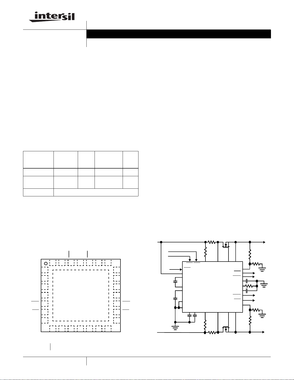
Pinout
SNS1
VO1
SS1
GT1
FLT1
PG1
CT1
ISL6173 (28 LD QFN) TOP VIEW
OCREF
CPQ-
EN2
BIAS
VS1
UV1
EN1
28 27 26 25 24 23 22
1
2
3
4
5
6
7
8 9 10 11 12 13 14
GND
PGND
RTR/LTCH
1
UV2
CPQ+
VS2
CPVDD
21
SNS2
20
VO2
19
SS2
GT2
18
17
FLT2
16
PG2
15
CT2
CAUTION: These devices are sensitive to electrostatic discharge; follow proper IC Handling Procedures.
1-888-INTERSIL or 1-888-468-3774
V1(in)
V2(in)
| Intersil (and design) is a registered trademark of Intersil Americas Inc.
All other trademarks mentioned are the property of their respective owners.
Rsns1
Rset1
VS1 SNS1
EN2
EN1
RTR/LTCH
BIAS
CPQ+
CPQCPVDD
PGND
GND
CT1 CT2 VS2 SNS2 GT2 VO2
FIGURE 1. TYPICAL APPLICATION
Copyright © Intersil Americas Inc. 2004-2006. All Rights Reserved
ISL6173
Rset2
Rsns2
GT1 VO 1
UV1
PG1
FLT1
SS1
OCREF
SS2
FLT2
PG2
UV2
V1(out)
V2(OUT)
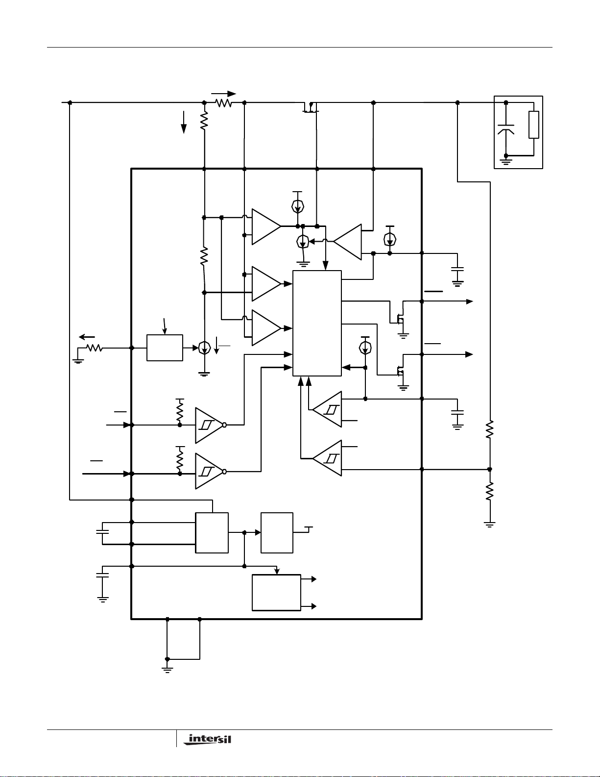
Block Diagram
www.BDTIC.com/Intersil
ISL6173
Io
Vin Vo
Limit
WOC
OC
42µA
QRsn s
10V
GT1
24µA
OC Timer
&
Logic
Soft Start
Amplifier
-
+
CPVDD
10µA
VO1
CPV DD
10µA
SS1
Css
FLT1
PG1
Ire f
Rref
OCREF
1. 178V
Cu rren t
Mi rror
I set
Rset
3K
VS1
Iref
SNS1
Cu rren t
Amplifier
-
+
-
+
Co mpar ato r
+
-
4
Co mpar ato r
LOAD
RT R/ LT CH
Cp
Cv
EN1
BI AS
CPQ +
CPQ -
CPV DD
10K
10K
PGND
BI AS
BI AS
Ch arge
Pump
GND
+
-
Timeout
Co mpar ato r
UV
Co mpar ato r
X2
Ch arg e
Pump
POR and
Bandgap
10V(o u t)
X2
633mV
1. 178V
1. 178V
-
633mV
+
ISL6173
CT 1
Ct
Rs1
UV1
Rs2
FIGURE 2. ISL6173 - INTERNAL BLOCK-DIAGRAM OF THE IC - CHANNEL ONE ONLY
2
FN9186.3
January 3, 2006
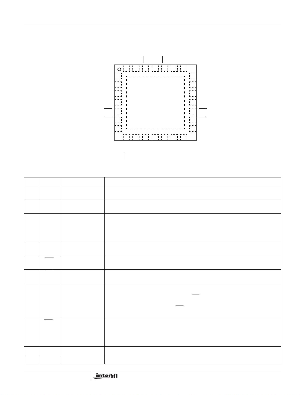
Pinout
www.BDTIC.com/Intersil
SNS1
ISL6173
28 LEAD QFN
TOP VIEW
OCREF
VS1
UV1
EN1
28 27 26 25 24 23 22
1
EN2
UV2
VS2
21
SNS2
CPVDD
20
VO2
19
SS2
GT2
18
17
FLT2
16
PG2
15
CT2
VO1
SS1
GT1
FLT1
PG1
CT1
2
3
4
5
6
7
8 9 10 11 12 13 14
GND
RTR/LTCH
CPQ-
PGND
BIAS
CPQ+
Pin Descriptions
PIN NAME FUNCTION DESCRIPTION
1 SNS1 Current Sense Input This pin is connected to the current sense resistor and control MOSFET Drain node. It provides
2 VO1 Output Voltage 1 This pin is connected to the control MOSFET switch source, which connects to a load. Internally, this
3 SS1 Soft-Start Duration Set
Input
current sense signal to the internal comparator and amplifier in conjunction with VS1 pin.
voltage is used for SS control.
A capacitor from this pin to ground sets the output soft-start ramp slope. This capacitor is charged by
the internal 10µA current source setting the soft-start ramp. The output voltage ramp tracks the SS
ramp by controlled enhancement of FET gate. Once ramp-up is completed, the capacitor continues
to charge to the CPVDD voltage rail. If common capacitor is used (by tying SS1, SS2 together and
the capacitor to GND from the connection) then both the outputs track each other as they ramp up.
4 GT1 Gate Drive Output Direct connection to the gate of the external N-Channel MOSFET. At turn-on the Gate will charge to
4 X Vbias or 10V(max) from the 24µA source.
5FLT1
Fault Output This is an open drain output. It asserts (pulls low) once the current regulation duration (determined
by the CTx timeout cap) has expired. This output is valid for Vbias>1V.
6PG1
Power Good Output This is an active low, open drain output. When asserted (logic zero), it indicates that the voltage on
UV1 pin is more than 643mV (633mV + 10mV hysteresis). This output is valid at VBIAS >1V.
7 CT1 Timer Capacitor A capacitor from this pin to ground controls the current regulation duration from the onset of current
regulation to channel shutdown (current limit time-out). Once the voltage on CTx cap reaches
the GATE output is pulled down and the FLT is asserted.
V
CT_Vth
The duration of current limit time-out = (C
When the OC comparator trips AND the RTR
*1.178)/10µA
TIM
/LTCH pin is pulled low, the IC’s faulty channel remains
shut down for 64 cycles (each cycle length is equal to the current limit time-out duration).
/
8RTR
LTC H
Retry Or Latch Input This input dictates the IC behavior (for either channel) under OC condition. If it is pulled high (or left
floating), the IC will shut down upon OC time-out. If it is pulled low, the IC will go into retry mode after
an interval determined by the capacitor on CTx pin. The faulting channel will remain shut down for
64 cycles and will try to come out of it on the 65th cycle. Each cycle length is determined by the
formula shown in CT pin description.
9 GND Chip Gnd This pin is also internally shorted to the metal tab at the bottom of the IC.
10 PGND Charge pump ground. Both GND and PGND must be tied together externally.
3
FN9186.3
January 3, 2006
ISL6173
www.BDTIC.com/Intersil
Pin Descriptions (Continued)
PIN NAME FUNCTION DESCRIPTION
11 CPQ- Charge Pump Capacitor
Low Side
12 BIAS Chip Bias Voltage Provides IC Bias. Should be 2V to 4V for IC to function normally. This pin can be powered from a
13 CPQ+ Charge Pump Capacitor
14 CPVDD Charge Pump Output This is the voltage used for some internal pullups and bias. Use of 0.47µF (minimum) is
15 CT2 Timer Capacitor Same function as pin 7
16 PG2
17 FLT2
18 GT2 Gate Drive Output Same as pin 4
19 SS2 Soft-Start Duration Set
20 VO2 Output Voltage 2 Same as pin 2
21 SNS2 Current Sense Input Same as pin 1
22 VS2 Current Sense
23 UV2 Undervoltage Monitor
High Side
Power Good Output Same function as pin 6
Fault Output Same as pin 5
Input
Reference
Input
Flying cap lowside.
supply voltage that is not being controlled. It is preferable to use 3.3V even if the channels being
controlled are 2.5V or lower because more gate drive voltage will be available to the MOSFETs.
Flying cap highside. Use of 0.1µF for 2.5V bias and 0.022µF for 3.3V bias is recommended.
recommended.
Same as pin 3
Voltage input for one of the two voltages. Provides a 20µA current source for the ISET series resistor
which sets the voltage to which the sense resistor IR drop is compared.
This pin is one of the two inputs to the undervoltage comparator. The other input is the 633mV
reference. It is meant to sense the output voltage through a resistor divider. If the output voltage
drops so that the voltage on the UV pin goes below 633mV, PG2
is deasserted.
24 EN2
25 OCREF Ref. Current Adj. Allows adjustment of the reference current through R
26 EN1
27 UV1 Undervoltage Monitor
28 VS1 Current Sense
Enable This is an active low input. When asserted (pulled low), the SS and gate drive are released and the
output voltage gets enabled. When deasserted (pulled high or left floating), the reverse happens.
resistor, thus setting the thresholds for CR, OC and WOC.
Enable Input Same as pin 24
Same as pin 23
Input
Same as pin 22
Reference
and the internal current regulation set
SET
4
FN9186.3
January 3, 2006
ISL6173
www.BDTIC.com/Intersil
Absolute Maximum Ratings Thermal Information
VBIAS . . . . . . . . . . . . . . . . . . . . . . . . . . . . . . . . . . . . . . . . . . . +5.5V
GTx, CPQ+ . . . . . . . . . . . . . . . . . . . . . . . . . . . . . . . . .-0.3V to +12V
, RTR/LTCH, SNSx, PGx, FLTx, VSx, CTx, UVx,
ENx
SSx, CPQ-, CPVDD. . . . . . . . . . . . . . . . . . . . . . . . -0.3V to 5.5VDC
Output Current . . . . . . . . . . . . . . . . . . . . . . . Short Circuit Protected
ESD Rating
Human Body Model (Per MIL-STD-883 Method 3015.7) . . .1750V
Machine Model (Per EIAJ ED-4701 Method C-111). . . . . . . . 125V
Charged Device Model (Per EOS/ESD DS5.3, 4/14/93) . . .1750V
Operating Conditions
VBIAS/VIN1 Supply Voltage Range. . . . . . . . . . . . +2.25V to +3.63V
Temperature Range (T
CAUTION: Stresses above those listed in “Absolute Maximum Ratings” may cause permanent damage to the device. This is a stress only rating and operation of the
device at these or any other conditions above those indicated in the operational sections of this specification is not implied.
NOTES:
is measured in free air with the component mounted on a high effective thermal conductivity test board with “direct attach” features. See
1. θ
JA
Tech Brief TB379.
2. All voltages are relative to GND, unless otherwise specified.
3. 1V (min) on the BIAS pin required for FLT
4. For θ
, the “case temp” location is the center of the exposed metal pad on the package underside.
JC
) . . . . . . . . . . . . . . . . . . . . . . . . 0°C to 85°C
A
to be valid.
Thermal Resistance (Typical, Notes 1, 4) θ
5x5 QFN Package . . . . . . . . . . . . . . . . 42 12.5
Maximum Junction Temperature . . . . . . . . . . . . . . . . . . . . . . . . 150°C
Maximum Storage Temperature Range . . . . . . . . . . . -65°C to 150°C
For recommended soldering conditions, see Tech Brief TB389.
(QFN - Leads Only)
(°C/W) θJC (°C/W)
JA
Electrical Specifications V
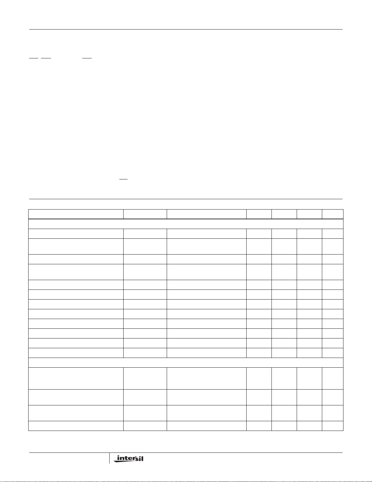
PARAMETER SYMBOL TEST CONDITIONS MIN TYP MAX UNIT
CURRENT REGULATION CONTROL
ISET Current I
Partial Temp Range I
Current Limit Amp Offset Voltage Vio_ft V
Partial Temp. Current Limit Amp Offset
Voltage
Current Regulation Threshold Voltage V
Current Regulation Accuracy V
Current Regulation Threshold Voltage V
Current Regulation Accuracy V
Current Regulation Threshold Voltage V
Current Regulation Accuracy V
CT Threshold Voltage V
CT Charging Current I
GATE DRIVE
GATE Response Time from WOC (Open) pd_woc_open GATE open
GATE Response Time from WOC
(Loaded)
GATE Response Time in Current
Regulation mode (Loaded)
GATE Turn-On Current IGATE GATE = 2V, V
Current I
SET
= 2.5V to +3.3V, VS = 1V ,TA = T
DD
SET_ft
SET_pt
Vio_pt V
CRVTH_1
CRVTH_1
CRVTH_2
CRVTH_2
CRVTH_3
CRVTH_3
CT_Vth
CT
pd_woc_load GATE = 1nF 100 ns
pd_cr_load GATE = 1nF
R
R
TJ = 25oC to 60oC
T
RISET = 1.25K, I
R RISET = 1.25K, I
RISET = 2.50K, I
R RISET = 2.50K, I
RISET = 0.499K, I
R RISET = 0.499K, I
100mV of overdrive on the WOC
comparator
120% Load Current
J
= 14.7kΩ 18.7 20 21.3 µA
OCREF
= 14.7kΩ
OCREF
- V
VS
SNS
- V
VS
SNS
= 25°C to 60°C
J
= 0°C - 85°C, Unless Otherwise Specified.
19 20 21 µA
with I
with I
VS
= 0A -2 2 mV
OUT
= 0A
OUT
= 20µA 23 25 27 mV
SET
= 20µA -8 +8 %
SET
= 20µA 48 50 52 mV
SET
= 20µA -4 +4 %
SET
= 20µA 8 10 12 mV
SET
= 20µA -20 +20 %
SET
= 2V, V
= 2.1V 21 24 27 µA
SNS
-1 1 mV
1.128 1.178 1.202 V
10 µA
3ns
5µs
5
FN9186.3
January 3, 2006
ISL6173
www.BDTIC.com/Intersil
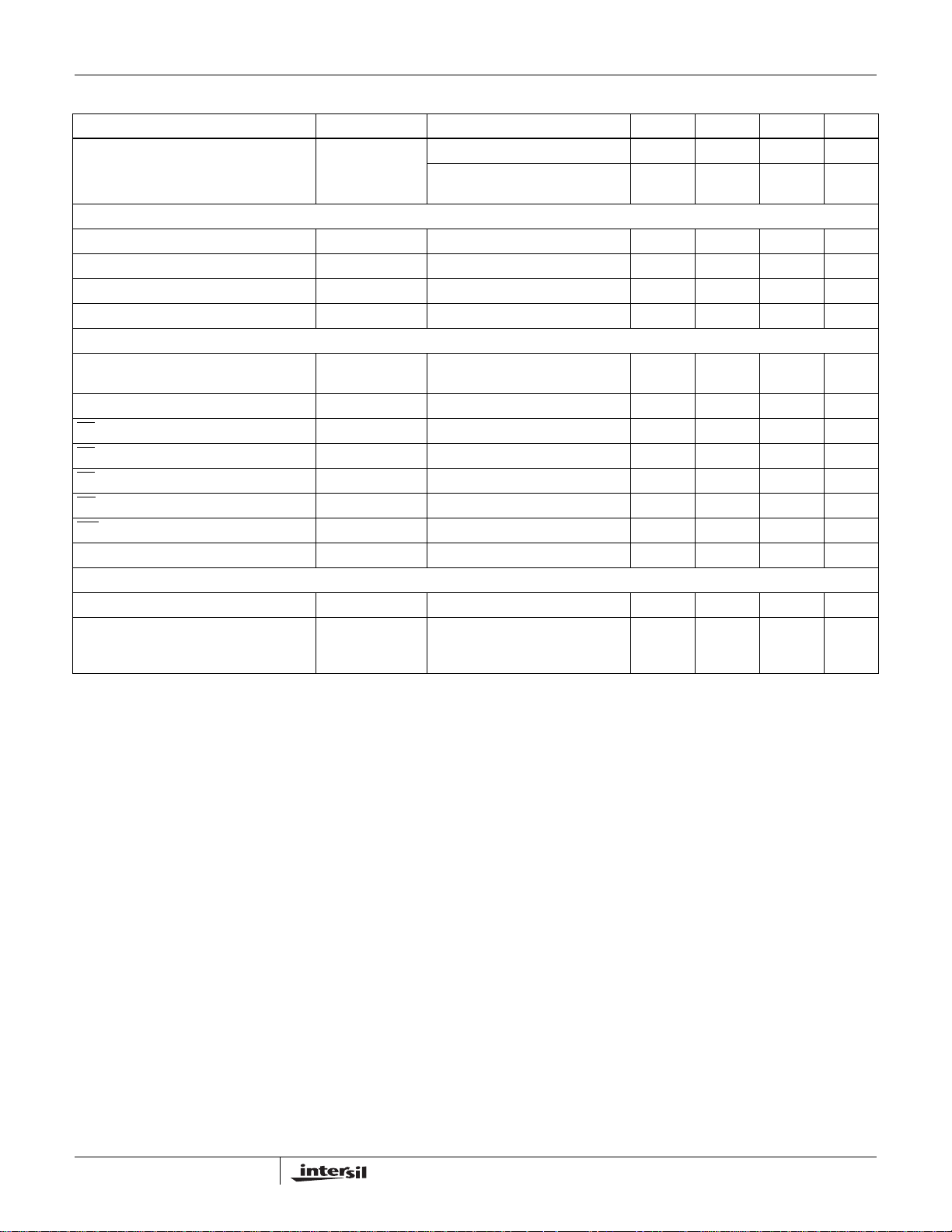
Electrical Specifications V
PARAMETER SYMBOL TEST CONDITIONS MIN TYP MAX UNIT
GATE Voltage V
BIAS
Supply Current I
POR Rising Threshold VIN_POR_L2H 2.12 V
POR Falling Threshold VIN_POR_H2L 2.10 V
POR Threshold Hysteresis VIN_POR_HYS 5 mV
I/O
Undervoltage Comparator Falling
Threshold
Undervoltage Comparator Hysteresis V
EN Rising Threshold PWR_Vth_R V
Falling Threshold PWR_Vth_F V
EN
Hysteresis PWR_HYST V
EN
PG Pull-Down Voltage
Pull-Down Voltage (Note 3)
FLT
Soft-Start Charging Current IQ_SS VSS = 1V 10 µA
CHARGE PUMP
CPVDD V_CPVDD V
CPVDD V_CPVDD V
= 2.5V to +3.3V, VS = 1V ,TA = T
DD
GATE
BIAS
V
UV_VTHF
UV_HYST
VOL_PG
VOL_FLT
Bias = 2.5V (see graph on page 7) 7.5 9.0 V
2.1 < Bias < 2.5
(see graph on page 7)
V
I
PG
I
FLT
T = 25°C
External User Load = 6mA
= 0°C - 85°C, Unless Otherwise Specified. (Continued)
J
8V
= 3.3V 9 17 mA
BIAS
620 635 650 mV
71625mV
= 2.5V 1.55 1.95 2.19 V
BIAS
= 2.5V 0.97 1.10 1.30 V
BIAS
= 2.5V 600 850 1100 mV
BIAS
= 8mA 0.047 0.4 V
= 8mA 0.047 0.4 V
= 3.3V 4.9 5.2 5.5 V
BIAS
BIAS
= 3.3V
5.0 V
6
FN9186.3
January 3, 2006

ISL6173
www.BDTIC.com/Intersil
Typical Performance Curves (at 25°C unless otherwise specified)
12
10
8
6
4
I_BIAS (mA)
2
0
1.0 1.4 1.7 2.0 2.3 2.9 3.2 3.7
CPQ = 22nF, C
V_BIAS(V)
PVDD
= 0.47µF
FIGURE 3. I_BIAS vs V_BIAS FIGURE 4. POR RISING THRESHOLD vs TEMPERATURE
10
9
8
7
6
(V)
5
GATE
4
V
3
2
1
0
2 2.1 2.2 2.3 2.4 2.5 2.6 2.7 2.8 2.9 3 3.1 3.2 3.3 3.5 3.7 3.8 3.9 4
FIGURE 5. V
CPQ = 22nF, C
V_BIAS (V)
vs V_BIAS FIGURE 6. V
GATE
PVDD
= 0.47µF
2.045
2.04
2.035
2.03
2.025
2.02
2.015
POR RISING (V)
2.01
2.005
2
-10 0 25 40 60 85
TEMPERATURE (°C)
10
9
8
7
6
(V)
5
4
GATE
V
3
2
1
0
2 2.1 2.2 2.3 2.4 2.5 2.6 2.7 2.8 2.9 3 3.1 3.2 3.3 3.5 3.7 3.8 3.9 4
CPQ = 0.1µF, C
V_BIAS (v)
vs V_BIAS
GATE
PVDD
= 0.47µF
(µA)
G
I
24.6
24.4
24.2
24
23.8
23.6
23.4
-10 0 25 40 60 85
TEMPERATURE (°C)
0.19
0.18
0.17
0.16
0.15
0.14
PG_VOL
0.13
0.12
0.11
0.1
-10 0 25 40 60 85
FIGURE 7. GATE DRIVE vs TEMPERATURE FIGURE 8. PG_VOL vs TEMPERATURE
7
TEMPERATURE (°C)
IPG = 8mA
FN9186.3
January 3, 2006

ISL6173
www.BDTIC.com/Intersil
Typical Performance Curves (at 25°C unless otherwise specified) (Continued)
10000
3
1000
(ns)
100
RESPONSE
T
10
1
0 0.1 0.47 1 4 8.7 14 222
C
(nF)
G
2.5
2
1.5
1
RESPONSE TIME (µs)
0.5
0
100 150 200 250 300
OC (% OF LIMIT)
FIGURE 9. WOC RESPONSE vs LOAD CAPACITANCE FIGURE 10. RESPONSE TIME vs IO*R
2.008
2.006
2.004
2.002
2
POR FALLING (V)
1.998
SNS
1.996
-10 0 25 40 60 85
TEMPERATURE (°C)
FIGURE 11. POR FALLING vs TEMPERATURE
8
FN9186.3
January 3, 2006

ISL6173
www.BDTIC.com/Intersil
Detailed Description of Operation
ISL6173 targets dual voltage hot-swap applications with a
bias of 2.1V to 3.6VDC and the voltages being controlled
down to 0.7VDC. The IC’s main function is to limit and
regulate the inrush current into the loads. This is achieved by
enhancing an external MOSFET in a controlled manner. In
order to fully enhance the MOSFET, the IC must provide
adequate gate to source voltage, which is typically 5V or
greater. Hence, the final steady-state voltage on Gate (GT)
pin must be 5V above the load voltage. Two internal chargepumps allow this to happen.
VIN
Q
1
O
V
CPVDD
-
+
10µA
10V
42µA
1
T
G
24µA
SOFT-
START
AMPLIFIER
FIGURE 12. SOFT-START OPERATION
Controlled Soft-Start
The output voltages are monitored through the Vo pins and
slew up at a rate determined by the capacitors on the Softstart (SS) pin, as illustrated in Figure 12. 24µA of gate
charge current is available. The soft-start amplifier controls
the output voltage by robbing some of the gate charge
current thus slowing down the MOSFET enhancement.
When the load voltage reaches its set level, as sensed by its
respective UV pin through an external resistor divider, the
Power Good (PG
) output goes active.
Current Monitoring and Protection
The IC monitors the load current (Io) by sensing the voltagedrop across the low value current sense resistor (R
which is connected in series with the MOSFET as shown in
the diagram on page 2, through Sense (SNS) and voltage
set (VS) pins. The latter is through a resistor, R
shown. Two levels of overcurrent detection are available to
protect against all possible fault scenarios. These levels are:
1. Current Limit or Current Regulation (CR)
2. Way Overcurrent (WOC)
VO
0
0
SS1
SET
+
-
SNS
, as
VIN
CPVDD
),
Each of these modes is described in detail as follows:
1. Current Limit or Current Regulation (CR) Mode: - When
the load current reaches the current regulation threshold, the
current amplifier loop closes and the circuit behaves like a
current source. The Current Limit Amplifier is a folded
cascode type with source follower output capable of pulling
down the gate very fast in response to fast overload
transients. The current regulation threshold is set by setting a
reference current, I
, through R
SET
by selecting an
SET
appropriate resistor between OCREF and GND, which sets
I
. The relationship between I
REF
4*I
SET
, where I
= Vocref/Rocref = 1.178/Rocref. I
REF
REF
and I
SET
is I
REF
=
REF
would typically be set at 80µA.
Selecting appropriate values for R
when I
Io*R
= ICR,
O
= I
SNS
SET*RSET
Vin Vo
Iset
ISL6173
FIGURE 13. CURRENT REGULATION OPERATION
+
Rset
-
3K
+
VS1
Rsns
Iref
4
-
CURRENT REGULATION
Iset*Rset = Io*Rsns
SNS1
CURRENT
LIMIT
AMPLIFIER
-
+
SET
MODE:
and R
10V
24µA
Q
such that
SNS
GT1
(EQ. 1)
The operating mode is shown in Figure 13. When the circuit
enters this mode, the OC comparator detects it and sets off
the timer. CT begins to charge from an internal 10µA current
source. The amount of time it takes for this cap to charge to
1.178V sets up the current regulation duration. Upon
expiration of this time-out period, the MOSFET gate is pulled
down quickly by the current limit amplifier, unless the load
current level had already dropped back to a level below the
current regulation threshold level prior to that. In that case, the
current regulation mode is no longer active, the MOSFET is
allowed to fully enhance and the IC discharges the C
RTR
/LTCH pin is left open or pulled to BIAS, the output
Cap. If
T
remains latched off after the expiration of the time-out period
determined by C
. If RTR/LTCH pin is pulled to GND, the IC
T
9
FN9186.3
January 3, 2006

ISL6173
www.BDTIC.com/Intersil
automatically retries to turn on the MOSFET after a wait
period, during which C
is charged and discharged 64 times
T
and the retry attempt takes place on the 65th time. This wait
period allows the MOSFET junction to cool down.
2. Way Overcurrent (WOC) Mode - This mode is designed
to handle very fast, very low impedance shorts on the load
side, which can result in very high di/dt. Typically, the current
limit set for this mode is 300% of the current regulation limit.
This mode uses a very fast comparator, which directly looks
at the voltage drop across R
and pulls the gate very
SNS
quickly to GND (as shown in Figure 14) and immediately
releases it. If the WOC is still present, the IC enters current
regulation mode and the rest of the current regulation
behavior follows as described earlier in undercurrent
regulation mode.
Vin
Iset
ISL6173
Rset
3K
Io
Rsns
-
SNS1
WOC
COMPARATOR
-
+
Q
GT1
GATE
PULLDOWN
CURRENT
25Ω
+
+
-
VS1
Vo
on this pin reaches 1.178V, the CR duration expires. Fault
(FLT
) pin goes active (pulls low), signaling the load of a fault
condition and the gate (GT) pin gets pulled low.
Retry vs Latched Fault Operational Modes:
RTR/LTCH pin dictates the IC behavior after the gate (GT)
pin pulls down following OC timeout expiration. If the
RTR
/LTCH pin is left floating, the gate pin will remain latched
off. It can only be released by de-asserting and reasserting
the enable (EN
) input. If RTR/LTCH pin is pulled to GND,
then the Retry mode will be activated. In this mode the IC will
automatically attempt to turn-on the MOSFET after a delay,
determined by the capacitor on CT pin. In the Retry mode,
the internal logic charges and discharges the CT cap 64
times during “wait” period. On the 65th time, the FLT output
clears during retry attempt. If the overcurrent condition
persists after the soft-start, the CT pin will again start
charging and the process repeats.
Bias and Charge Pump Voltages:
The BIAS pin feeds the chip bias voltage directly to the first
of the two internal charge pumps, which are cascaded. The
output of the first charge pump, in addition to feeding the
second charge pump, is accessible on the CPVDD pin. The
voltage on the CPVDD pin is approximately 5V. It also
provides power to the POR and band-gap circuitry as shown
in the block diagram. A capacitor connected externally
across CPQ+ and CPQ- pins of the IC is the “flying” cap for
the charge-pump.
The second charge-pump is used exclusively to drive the
gates of the MOSFETs through the 24µA current sources,
one for each channel. The output of this charge pump is
approximately 10V as shown in the block diagram.
FIGURE 14. WOC OPERATION
Additionally, as shown in the block diagram, there is also an
“OC comparator”, which also looks at the Rsense voltage
drop. When this drop exceeds the Current Limit set point, it
triggers the timeout circuit, which starts ticking and CTx is
allowed to charge. If the current limit condition remains in
effect until after the time-out period expires (CTx voltage
exceeding 1.178V), the gate of the MOSFET is pulled down,
the SSx capacitor is discharged, FLT
SS sequence is allowed to begin after ENx
keeping the RTR
/LTCH pin pulled low.
is asserted and a new
recycle or by
The voltage on OCREF pin is the same as the internal bandgap reference voltage, which is 1.178V (nominal). A resistor
to GND from this pin sets the reference current (and hence
the reference voltage) for the current limit amplifier and
OC/WOC comparators. The current regulation (CR) duration
is set by the capacitor on CT pin to GND. Once the voltage
10
Tracking
CH1: VO1, CH2: VO2, T = 2ms/DIV, CSS = 0.066µF
FIGURE 15. TRACKING MODE WAVEFORMS
January 3, 2006
FN9186.3

ISL6173
www.BDTIC.com/Intersil
The two channels can be forced to track each other by
simply tying their SS pins together and using a common SS
capacitor. In addition, their EN
together. Typical Start-up waveforms in this mode are shown
in Figure 15. If one channel goes down for any reason, the
other one will too. One important thing to note here is that
only the overcurrent latch-off mode will work. Auto-retry
feature WILL NOT work. Retry must be controlled manually
through EN
.
pins also must be tied
Typical Hot-plug Power Up Sequence
1. When power is applied to the IC on the BIAS pin, the first
charge pump immediately powers up.
2. If the BIAS voltage is 2.1V or higher, the IC comes out of
POR. Both SS and CT caps remain discharged and the
gate (GT) voltage remains low.
3. ENx
pin, when pulled low (below it’s specified threshold),
enables the respective channel.
4. SSx cap begins to charge up through the internal 10µA
current source, the gate (GT) voltage begins to rise and
the corresponding output voltage begins to rise at the
same rate as the SS cap voltage. This is tightly controlled
by the soft-start amplifier shown in the block diagram.
5. SS cap begins to charge but the corresponding CTx cap
is held discharged.
6. Fault (FLT) remains deasserted (stays high) and the
output voltage continues to rise.
7. If the load current on the output exceeds the set current
limit for greater than the OC timeout period, FLT gets
asserted and the channel shutdown occurs.
8. If the voltage on UV pin exceeds 633mV threshold as a
result of rising Vo, the Power Good (PG) output goes
active.
9. At the end of the SS interval, the SS cap voltage reaches
CPVDD and remains charged as long as EN remains
asserted or there is no other fault condition present that
would attempt to pull down the gate.
State Diagram
This is shown in Figure 16. It provides a quick overview of
the IC operation and can also be used as a troubleshooting
road map.
11
FN9186.3
January 3, 2006

IC Operation State Diagram
www.BDTIC.com/Intersil
ISL6173
No
Po w e r
Apply Power
Bias >1V
PG
&
FLT
Out put s
Valid
Bias>2V
Io> >ICR
(WOC)
Gat e
Pulldow n
Output
Voltage
Available
Vuv >645mVVuv<633mV
PG
Asserted
Io> ICR
FLT
Cleared
EN A s s er t e d
Sof t Star t
(Tss)
Run
OC Timer
(Toc)
EN De - as s e r te d
Io> ICR
Current
Limit
Mo de
Io> =Ic r
AND
t>Toc
FLT
Asserted
Count 64
Pu l s e s
&
Re se t
RTR/LTCH = L
Res et &
Latch
Of f
Stat e
RTR/LTCH = H
FIGURE 16.
12
FN9186.3
January 3, 2006

ISL6173
www.BDTIC.com/Intersil
Applications Information
Selection of External Components
The typical application circuit of Figure 2 has been used for
this section, which provides guidelines to select the external
component values.
MOSFET (Q1)
This component should be selected on the basis of its
r
voltage) and the effective input gate capacitance (Ciss). One
needs to ensure that the combined voltage drop across the
Rsense and r
(including transients) will still keep the output voltage above
the minimum required level. Power dissipation in the device
under short circuit condition should also be an important
consideration especially in auto-retry mode (RTR
pulled low). Using ISL6173 in latched off mode results in
lower power dissipation in the MOSFET.
Ciss of the MOSFET influences the overcurrent response
time. It is recommended that a MOSFET with Ciss of less
than 10nF be chosen. Ciss will also have an impact on the
SS cap value selection as seen later.
Current Sense Resistor (R
The voltage drop across this resistor, which represents the
load current (Io), is compared against the set threshold of
the current regulation amplifier. The value of this resistor is
determined by how much combined voltage drop is tolerable
between the source and the load. It is recommended that at
least 20mV drop be allowed across this resistor at max load
current. This resistor is expected to carry maximum full load
current indefinitely. Hence, the power rating of this resistor
must be greater than I
This resistor is typically a low value resistor and hence the
voltage signal appearing across it is also small. In order to
maintain high current sense accuracy, current sense trace
routing is critical. It is recommended that either a four wire
resistor or the following routing method be used:
specification at the expected Vgs (gate to source
DS(ON)
at the desired maximum current
DS(ON)
/LTCH pin
)
SNS
2
*R
O(MAX)
LOAD CURRENT CARRYING
FIGURE 17. RECOMMENDED CURRENT SENSE RESISTOR
PCB LAYOUT
TRACES
CURRENT
SENSE
TRACES
SNS
.
R
SNS
Current Set Resistor (R
SET)
This resistor directly sets the threshold for the current
regulation amplifier and indirectly sets the same for the OC
and WOC comparators in conjunction with R
R
has been selected, use Equation 1 (on page 9) to
SNS
calculate R
Reference Current Set Resistor (R
. Use 20µA for I
SET
in a typical application.
SET
REF
SNS
)
. Once
This resistor sets up the current in the internal current
source, I
/4, shown in Figure 2 for the comparators. The
REF
voltage at the OCREF pin is the same as the internal
bandgap reference. The current (I
) flowing through this
REF
resistor is simply:
I
= 1.178/R
REF
This current, I
REF
, should be set at 80µA to force 20µA in the
REF
internal current source as shown in Figure 2, because of the
4:1 current mirror. This equates to the resistor value of
14.7K.
Selection of Rs1 and Rs2
These resistors set the UV detect point. The UV comparator
detects the undervoltage condition when it sees the voltage
at UV pin drop below 0.633V. The resistor divider values
should be selected accordingly.
Charge Pump Capacitor Selection (CP and CV)
CP is the “flying cap” and CV is the smoothing cap of the
charge pump, which operates at 450kHz set internally. The
output resistance of the charge pump, which affects the
regulation, is dependent on the C
value and its ESR,
P
charge-pump switch resistance, and the frequency and ESR
of the smoothing cap, C
.
V
It is recommended that CP be kept within 0.022µF
(minimum) to 0.1µF (maximum) range. Only ceramic
capacitors are recommended. Use 0.1µF cap if CPVDD
output is expected to power an external circuit, in which case
the current draw from CPVDD must be kept below 10mA.
C
should at least be 0.47µF (ceramic only). Higher values
V
may be used if low ripple performance is desired.
Time-out Capacitor Selection (CT)
This capacitor controls the current regulation time-out
period. As shown in Figure 2, when the voltage across this
capacitor exceeds 1.178V, the time-out comparator detects it
and pulls down the gate voltage thus shutting down the
channel. An internal 10µA current source charges this
capacitor. Hence, the value of this capacitor is determined by
the following equation:
C
= (10µA * T
T
Where,
T
= Desired time-out period.
OUT
OUT
)/1.178
13
FN9186.3
January 3, 2006

ISL6173
www.BDTIC.com/Intersil
Soft-Start Capacitor Selection (CSS)
The rate of change of voltage (dv/dt) on this capacitor, which
is determined by the internal 10µA current source, is the
same as that on the output load capacitance. Hence, the
value of this capacitor directly controls the inrush current
amplitude during hot swap operation.
C
= CO*(10µA/I
SS
Where,
C
= Load Capacitance
O
I
INRUSH
I
INRUSH
the load capacitance charging current. If the dc steady-state
load remains disabled until after the soft-start period expires
(PGx
then only the capacitor charging current should be used as
I
INRUSH
of that of Ciss of the MOSFET to ensure proper soft-start
operation. This is because the Ciss is charged from 24µA
current source whereas the Css gets charged from a 10µA
current source (please refer to Figure 12). In order to make
sure both Vss and Vo track during the soft-start, this
condition is necessary.
= Desired Inrush Current
is the sum of the dc steady-state load current and
could be used as a load enable signal, for example),
. The Css value should always be more than (1/2.4)
INRUSH
)
ISL6173 Evaluation Platform
The ISL6173EVAL1 is the primary evaluation board for this
IC. The board is a standalone evaluation platform and it only
needs input bias and test voltages. The schematic for this
board is shown in Figures 20 and 21. The component
placement diagram is shown in Figure 22.
The evaluation board has been designed with a typical
application and accessibility to all the features in mind to
enable a user to understand and verify these features of the
IC. The circuit is designed for 2A for each input rail but it can
easily be scaled up or down by adjusting some component
values. LED indicators are provided to indicate Fault and
Power Good status. Switches are there to perform Enable
function for each channel, to select auto-retry or latchoff
mode and to check WOC and CR modes.
There are two input voltages, one for each channel plus
there is “+5V” input. The latter is to test the pull-up capability
of FLT
and PG outputs to +5V and also to power the LEDs
and the dynamic load circuitry. ISL6173 does not require 5V.
The outputs are brought out to banana sockets to allow
external loading if desired.
J1 and J3 are wire jumpers. A user can replace them with
wire loops to attach a scope current probe. However, doing
so may reduce the di/dt enough to prevent WOC comparator
from tripping. The internal current regulation amplifier is fast
enough to respond to very fast di/dt. Hence, it is advisable to
use the on board dynamic load circuitry, as will be described,
if a user wants to check the WOC performance.
The dynamic load circuitry, shown in Figure 21, is included
on the board on both channels to ensure minimum
inductance in the current flow path. Two sets of load are
available per output:
1) CR Load: This load is set at 1Ω (approximately 3.3A for
3.3V output), which is higher than the 2.2A of CR limit but
less than WOC limit (6.6A) set on the board.
2) WOC Load: This load is set at 340mΩ, which is roughly
10A for 3.3V supply. This is higher than 6.6A WOC limit set
on the board.
A function/pulse generator is required to activate the
dynamic load circuitry. The function/pulse generator should
have adjustable pulse-width (3ms), single pulse (manual
trigger) and 5V pulse amplitude capability. Agilent model
No: 33220A or equivalent is a good choice. The function
generator needs to be connected through a co-ax cable to
J11 or J12 for channel 1 or channel 2 respectively. WOC or
CR load can be activated by turning SW4 or SW5 (channel
1) and SW6 or SW7 (channel 2) ON followed by applying the
pulse generator to turn on an appropriate load.
The load circuit consists of a MOSFET driver (EL7202),
MOSFET (IRF7821) and surface mount load resistors. The
MOSFET drivers, U2 and U3, respond to a pulse from the
generator to turn on the MOSFET for the duration of the
pulse, which should be set less than the timeout period
described in “Time-out Capacitor Selection”. On this board
the timeout capacitor value is 0.15µF, which corresponds to
a timeout period of 17.67ms.
One way to tell if the WOC mode is active would be by
looking at the Gate waveform of the control MOSFET (M1 or
M2). The WOC comparator when tripped, pulls down the
Gate hard. The following waveform shows WOC operation:
Pins SS1 and SS2 of the IC are available on header J2 as
test points so that they can be tied together to achieve
tracking between Vo1 and Vo2. Both the Enable (EN
switches (SW1 and SW2) must be turned ON to check this
function.
Each channel is preloaded with capacitive load. Extra load
can be externally applied as required.
14
)
FN9186.3
January 3, 2006

FIGURE 18. WOC OPERATION
www.BDTIC.com/Intersil
Channel 1 is Vgate, Channel 2 is the pulse generator output
and Channel 3 is Vout. Note how Vgate gets immediately
pulled down to zero volts up on load application.
ISL6173
In CR mode, however, Vgate always remains above zero
volts because WOC comparator never trips. This can be
seen on the following scope shot:
FIGURE 19. CURRENT REGULATION OPERATION
It is also important to note that in WOC mode, although
Vgate gets pulled down to zero initially, the gate is quickly
released and slowly rises until the CR amplifier takes control.
15
FN9186.3
January 3, 2006

ISL6173
www.BDTIC.com/Intersil
Bill of Materials for ISL6173 Eval 1 Board
ITEM QTY REFERENCE PART PKG MFG P/N MANUFACTURER
1 2 C1, C18 220µF Leaded UPM1E221MPH6 or eq Nichicon
2 2 C2, C17 47µF Leaded UPM1E470MEH or eq Nichicon
3 2 C3, C4 0.1µF 0805 Any
4 2 C5, C6 1000pF 0805 Any
5 2 C9, C10 0.033µF 0805 Any
6 2 C11, C12 0.15µF 0805 Any
7 1 C13 0.47µF 0805 Any
8 1 C14 2.2µF 1206 Any
9 2 C19, C20 0.01µF 0805 Any
10 1 C21 10µF 7343 Any
11 1 C22 0.022µF 0805 Any
12 2 D1, D6 MBR130P SMA MBR130P ON Semi
13 2 D3, D4 LED GRN 1206 PG1101W Stanley
14 2 D2, D5 LED RED 1206 BR1101W Stanley
15 1 J2 2 Pin Header Any
16 2 J1, J3 Jumper Any
17 2 J11, J12 BNC Jack
18 6 M1, M2, M3, M4, M5, M6 IRF7821 SO8 IRF7821 International
19 10 RS1, RS2, R10, R12, R30, R31 1K 0805 Any
R55, R56, R57, R58
20 6 R1, R27, R49, R50, R51, R52 0.01 2512 Any
21 4 R2, R3, R25, R26 390 0805 Any
22 1 R8 3.57K 0805 Any
23 1 R9 2.55K 0805 Any
24 1 R11 14.7K 0805 Any
25 3 R14, R15, R20 0 0805 Any
26 4 R16, R17, R18, R19 10K 0805 Any
27 2 R29, R32 1.1K 0805 Any
28 4 R33, R34, R35, R36 10 0805 Any
29 6 R37, R38, R42, R43, R44, R45 1 2512 Any
30 10 R39, R40, R41, R46, R47, R48 5 2512 Any
R61, R62, R63, R64
31 2 R53, R54 100 1206 Any
32 2 R59, R60 49.9 0805 Any
34 1 U1 ISL6173 QFN28 5x5 ISL6172 Intersil
35 2 U2, U3 EL7202/SO SO8 Intersil
38 7 SW5, SW6, SW7, SW8, SW9,
SW10, SW11
Toggle Switch GT11MCKE C & K
Rectifier
16
FN9186.3
January 3, 2006

Schematic, ISL6173 Eval1
www.BDTIC.com/Intersil
220µF
5V
J4
3.3V
C1
5V
J5
GND_IN
J6
1
Vi_2
J7
1
2.5V
Vi_1
1
1
2
J1
CON2
C4
0.1µF
1
CON2
C18
J3
220µF
1
2
17
Vi_1
Vi_2
0.1µF
SW1
SW2
OPEN = Disable
CLOSE = Enable
C3
TP11
1
TP12
SW3
1
OPEN = Latch
CLOSE = Retry
R20
0
C14
2.2µF
RS2
1K
RS1
1K
C22
0.022µF
C13
0.47µF
TP9
1
TP10
1
TP6
1
C19
0.01µF
0.15µF
8
RTR/LTCH
12
BIAS
13
CPQ+
11
CPQ-
14
CPVDD
10
PGND
9
GND
C11
TP5
1
C20
0.01µF
24
EN126EN2
CT1
VS1
ISL6173
CT215VS222SNS221GT2
7
C12
0.15µF
1000pF
IRF7821
0.01
R29
1.1K
NO STUFF
28
U1
R32
1.1K
C6
R27
0.01
IRF7821
M1
5678123
R1
C5
1000pF
1
SNS1
NO STUFF
M2
5678123
TP1
1
4
GT1
OCREF
18
R14
0
VO1
UV1
PG1
FLT1
SS1
GND1
PG2
FLT2
SS2
UV2
VO2
R15
0
R10
TP16
R3
390
D3
LED55B/TO
D4
PG2
LED55B/TO
R26
390
J8
VO1
1
D1
MBR130P
GND_OUT
J9
1
J10
1
D6
MBR130P
VO1
ISL6173
VO2
VO2
TP2
TP3
1
C2
R53
5V
C17
47µF
TP7
47µF
1
TP17
100
5V
TP18
1
1
R54
100
5V
R2
TP13
1
390
D2
FLT1
LED55B/TO
D5
FLT2
LED55B/TO
R25
390
C21
10µF
R16
R17
10K
10K
1
R18
R19
10K
10K
1
TP14
TP15
1
4
1K
R8
3.57K
2
TP4
1
C10
0.033µF
R11
14.7K
C9
0.033µF
R12
1K
R30
R31
TP8
1
R9
2.55K
1K
1K
1
2
J2
CON2
27
6
5
3
25
29
16
17
19
23
20
1
4
January 3, 2006
FN9186.3
FIGURE 20.

Schematic, ISL6173 Eval1 (Continued)
www.BDTIC.com/Intersil
VO1
TP28
1
R63
R64
5
R37
R38
1
TP31
R35
10
R33
10
M3
IRF7821
4
1
2
3
4
R44
1
M5
IRF7821
4
U2
NC1
IN2
GND
IN2_
EL7202/SO
TP32
R59
49.9
R60
49.9
1
SW4
R55
1K
1
SW6
R57
1K
18
VO2
1
1
1
January 3, 2006
FN9186.3
1
1
2
4
J11
3
1
2
4
J12
3
TP33
TP34
TP35
TP36
1
OUTA
OUTB
R43
1
5
6
7
8
1
2
3
NC8
5
6
7
8
1
2
3
R42
1
TP30
1
SW5
TP26
1
R49
01
5V
8
7
6
V+
5
TP19
1
R45
1
TP20
1
TP21
1
R51
01
1
NC1
2
IN2
3
GND
4
IN2_
SW7
U3
EL7202/SO
NC8
OUTA
OUTB
R56
1K
R58
1K
8
7
6
V+
5
5
R34
10
R61
R62
5
5
M6
IRF7821
R36
4
10
5V
R40
5
M4
IRF7821
4
R47
5
R39
R46
5
TP27
1
R41
5
5
TP29
1
5
6
7
8
1
2
TP25
3
1
R50
01
ISL6173
TP24
1
R48
5
TP23
R52
01
1
1
TP22
5
6
7
8
1
2
3
FIGURE 21.

ISL6173 Eval 1 - Component Layout
www.BDTIC.com/Intersil
19
ISL6173
January 3, 2006
FN9186.3
FIGURE 22.

ISL6173
www.BDTIC.com/Intersil
Quad Flat No-Lead Plastic Package (QFN)
Micro Lead Frame Plastic Package (MLFP)
2X
0.15
C
E1/2
E1
A2
A
A1
8
E2
7
8
9
CORNER
OPTION 4X
A1
A
E/2
9
/ /
9
(Ne-1)Xe
REF.
E
B
0.10 C
0.08
0.152XB
C
C
A
6
INDEX
AREA
AREA
2X
2X
SEATING PLANE
(DATUM B)
(DATUM A)
INDEX
AREA
0.15
6
C
4X
C
4X P
4X P
NX L
1
2
3
B
0
8
9
N
TOP VIEW
AC0.15
SIDE VIEW
NX b
N
e
(Nd-1)Xe
BOTTOM VIEW
D
D1
D2
REF.
5
D/2
D1/2
5
D2
2
NX b
0.10 BAMC
7
NX k
N
1
2
3
A3
E2/2
L28.5x5
28 LEAD QUAD FLAT NO-LEAD PLASTIC PACKAGE
(COMPLIANT TO JEDEC MO-220VHHD-1 ISSUE I)
MILLIMETERS
SYMBOL
A 0.80 0.90 1.00 A1 - 0.02 0.05 A2 - 0.65 1.00 9
A3 0.20 REF 9
b 0.18 0.25 0.30 5,8
D 5.00 BSC -
D1 4.75 BSC 9
D2 2.95 3.10 3.25 7,8
E 5.00 BSC E1 4.75 BSC 9
E2 2.95 3.10 3.25 7,8
e 0.50 BSC k0.20 - - L 0.50 0.60 0.75 8
N282
Nd 7 3
Ne 7 3
P- -0.609
θ --129
NOTES:
1. Dimensioning and tolerancing conform to ASME Y14.5-1994.
2. N is the number of terminals.
3. Nd and Ne refer to the number of terminals on each D and E.
4. All dimensions are in millimeters. Angles are in degrees.
5. Dimension b applies to the metallized terminal and is measured
between 0.15mm and 0.30mm from the terminal tip.
6. The configuration of the pin #1 identifier is optional, but must be
located within the zone indicated. The pin #1 identifier may be
either a mold or mark feature.
7. Dimensions D2 and E2 are for the exposed pads which provide
improved electrical and thermal performance.
NOTESMIN NOMINAL MAX
Rev. 1 11/04
8. Nominal dimensions are provided to assist with PCB Land Pattern
C
L
SECTION "C-C"
C
L
Design efforts, see Intersil Technical Brief TB389.
9. Features and dimensions A2, A3, D1, E1, P & θ are present when
Anvil singulation method is used and not present for saw
L
10
L1
e
CC
TERMINAL TIP
FOR ODD TERMINAL/SIDE FOR EVEN TERMINAL/SIDE
e
L1
L
10
singulation.
All Intersil U.S. products are manufactured, assembled and tested utilizing ISO9000 quality systems.
Intersil Corporation’s quality certifications can be viewed at www.intersil.com/design/quality
Intersil products are sold by description only. Intersil Corporation reserves the right to make changes in circuit design, software and/or specifications at any time without
notice. Accordingly, the reader is cautioned to verify that data sheets are current before placing orders. Information furnished by Intersil is believed to be accurate and
reliable. However, no responsibility is assumed by Intersil or its subsidiaries for its use; nor for any infringements of patents or other rights of third parties which may result
from its use. No license is granted by implication or otherwise under any patent or patent rights of Intersil or its subsidiaries.
For information regarding Intersil Corporation and its products, see www.intersil.com
20
FN9186.3
January 3, 2006
 Loading...