

Page 1
®
www.BDTIC.com/Intersil
ISL6144
Data Sheet February 15, 2007
High Voltage ORing MOSFET Controller
The ISL6144 ORing MOSFET Controller and a suitably sized
N-Channel power MOSFET(s) increases power distribution
efficiency and availability when replacing a power ORing diode
in high current applications.
In a multiple supply, fault tolerant, redundant power distribution
system, paralleled similar power supplies contribute equally to
the load current through various power sharing schemes.
Regardless of the scheme, a common design practice is to
include discrete ORing power diodes to protect against reverse
current flow should one of the power supplies develop a
catastrophic output short to ground. In addition, reverse current
can occur if the current sharing scheme fails and an individual
power supply voltage falls significantly below the others.
Although the discrete ORing diode solution has been used for
some time and is inexpensive to implement, it has some
drawbacks. The primary downside is the increased power
dissipation loss in the ORing diodes as power requirements for
systems increase. Another disadvantage when using an ORing
diode would be failure to detect a shorted or open ORing diode,
jeopardizing power system reliability . An open diode reduces
the system to single point of failure while a diode short might
pose a hazard to technical personnel servicing the system
while unaware of this failure.
The ISL6144 can be used in 10V to 75V systems having similar
power sources and has an internal charge pump to provide a
floating gate drive for the N-Channel ORing MOSFET . The High
Speed (HS) Comparator protects the common bus from
individual power supply shorts by turning off the shorted feed’s
ORing MOSFET in less than 300ns and ensuring low reverse
current.
An external resistor-programmable detection level for the HS
Comparator allows users to set the N-Channel MOSFET
“V
- VIN” trip point to adjust control sensitivity to power
OUT
supply noise.
The Hysteretic Regulating (HR) Amplifier provides a slow turn-
off of the ORing MOSFET. This turn-off is achieved in less than
100μs when one of the sourcing power supplies is shutdown
slowly for system diagnostics, ensuring zero reverse current.
This slow turn-off mechanism also reacts to output voltage
droop, degradation, or power-down.
An open drain FAUL T
The fault detection circuitry covers different types of failures;
including dead short in the sourcing supply, a short of any two
ORing MOSFET terminals, or a blown fuse in the power
distribution path.
pin will indicate that a fault has occurred.
FN9131.3
Features
• Wide Supply Voltage Range +10V to +75V
• Transient Rating to +100V
• Reverse Current Fault Isolation
• Internal Charge Pump Allows the use of N-Channel
MOSFET
• HS Comparator Provides Very Fast <0.3µs Response
Time to Dead Shorts on Sourcing Supply. HS Comparator
also has Resistor-adjustable Trip Level
• HR Amplifier allows Quiet, <100µs MOSFET Turn-off for
Power Supply Slow Shut Down
• Open Drain, Active Low Fault Output with 120µs Delay
• Provided in Packages Compliant to UL60950 (UL1950)
Creepage Requirements
• QFN Package:
- Compliant to JEDEC PUB95 MO-220
QFN - Quad Flat No Leads - Package Outline
- Near Chip Scale Package footprint, which improves
PCB efficiency and has a thinner profile
• Pb-Free Plus Anneal Available (RoHS Compliant)
Applications
• ORing MOSFET Control in Power Distribution Systems
• N + 1 Redundant Distributed Power Systems
• File and Network Servers (12V and 48V)
• Telecom/Datacom Systems
Ordering Information
PART
NUMBER
ISL6144IV* ISL61 44IV -40 to +105 16 Ld TSSOP M16.173
ISL6144IVZA*
(See Note)
ISL6144IR* ISL 6144IR -40 to +105 20 Ld 5x5 QFN L20.5x5
ISL6144IRZA*
(See Note)
NOTE: Intersil Pb-free plus anneal products employ special Pb-free
material sets; molding compounds/die attach materials and 100% matte
tin plate termination finish, which are RoHS compliant and compatible
with both SnPb and Pb-free soldering operations. Intersil Pb-free
products are MSL classified at Pb-free peak reflow temperatures that
meet or exceed the Pb-free requirements of IPC/JEDEC J STD-020.
*Add “-T” suffix for tape and reel.
PART
MARKING
ISL61 44IVZ -40 to +105 16 Ld TSSOP
ISL6144 IRZ -40 to +105 20 Ld 5x5 QFN
TEMP.
RANGE
(°C) PACKAGE
(Pb-Free)
(Pb-Free)
PKG.
DWG. #
M16.173
L20.5x5
1
CAUTION: These devices are sensitive to electrostatic discharge; follow proper IC Handling Procedures.
1-888-INTERSIL or 1-888-468-3774
| Intersil (and design) is a registered trademark of Intersil Americas Inc.
Copyright © Intersil Americas Inc. 2004, 2006-2007. All Rights Reserved
All other trademarks mentioned are the property of their respective owners.
Page 2
ISL6144
www.BDTIC.com/Intersil
Pinouts
GATE
VIN
HVREF
NC
NC
NC
NC
GND
ISL6144
(16 LD TSSOP)
TOP VIEW
1
2
3
4
5
6
7
8
16
VOUT
15
COMP
1
14
VSET
13
NC
12
NC
11
NC
10
NC
9
FAULT
VIN
HVREF
NC
NC
NC
2
3
4
5
ISL6144
(20 LD 5x5 QFN)
TOP VIEW
NC
20 19 18 17 16
678910
NC
GATE
GND
NC
NC
NC
FAULT
NC
NC
15
VOUT
14
COMP
13
VSET
12
NC
NC
11
Pin Descriptions
TSSOP
PIN #
1 19 GATE External FET Gate Drive Allows active control of extern al N -Chan nel FET ga te to p erform ORing
21
3 2 HVREF Chip High Voltage Reference Low side of floating high voltage reference for all of the HV chip circuitry.
8 7 GND Chip Ground Reference Chip ground reference point.
99FAULT
14 13 VSET Low Side Connection for Trip Level Resistor connected to COMP provides adjustable “Vd-Vs” trip level along
15 14 COMP High Side Connection for HS
16 15 VOUT Chip Bi as and Loa d Co nn ec ti on Provides the second sensing node for external FET control and chip output
4-7,
10-13
QFN
PIN # SYMBOL FUNCTION DESCRIPTION
function.
VIN
Power Supply Connection Chip bias input. Also provides a sensing node for external FET control.
Fault Output Provides an open drain active low output as an indication that a fault has
V
occurred: GATE is OFF (GATE <
resulting in
V
- V
> 0.41V.
OUT
IN
+ 0.37V) or other types of faults
IN
with pin COMP.
provides sense point for the adjustable Vd-Vs
OUT
Comparator Trip Level
Resistor connected to V
trip level along with pin VSET.
bias.
3-6, 8,
NC No Connection
10-12,
16-18, 20
2
FN9131.3
February 15, 2007
Page 3
General Application Circuit
www.BDTIC.com/Intersil
+
-
ISL6144
LOAD “+48V”
AC/DC
1
AC POWER
AC/DC
N + 1
5V
5V
VIN
ISL6144
HVREF
FAULT
VIN
HVREF
FAULT
GATE
GND
GATE
ISL6144
GND
VOUT
COMP
VSET
VOUT
COMP
VSET
DC/DC
1
+48VDC BUS
DC/DC
N + 1
5V
5V
VIN
HVREF
FAULT
VIN
HVREF
FAULT
GATE
ISL6144
GND
GATE
ISL6144
GND
VOUT
COMP
VSET
LOAD “+12V”
+12VDC BUS
VOUT
COMP
VSET
NOTES:
5. AC/DC 1 through (N + 1) are multistage AC/DC converters which include AC/DC rectification stage and a DC/DC Converter with a +48VDC
output (also might include a Power Factor Correction stage).
6. DC/DC Converter 1 through (N + 1) are DC/DC converters to provide additional Intermediate Bus
7. Load “+12V” and Load “+48V” might include other DC/DC converter stages to provide lower voltages such as ±15V, ±5V, +3.3V, +2.5V,
+1.8V etc.
8. Fuse location might vary depending on power system architecture.
FIGURE 1. ISL6144 GENERAL APPLICATION CIRCUIT IN A DISTRIBUTED POWER SYSTEM
3
FN9131.3
February 15, 2007
Page 4
Simplified Block Diagram
www.BDTIC.com/Intersil
ISL6144
SOURCE 2
10V TO 75V
SOURCE 1
10V TO 75V
C
C
1
VIN GATE
GATE LOGIC AND
CHARGE PUMP
1
DETECTION
5.5V
LEVEL
SHIFT
2A*
5mA
HVREF
VIN
HVREF
FAULT
FAULT
HS
COMP
D2*
GATE
ISL6144
GND
-
+
REG
AMPLIFIER
-
+
VOUT
COMP
VSET
D1*
F2**
R
1C2
R
2
* D
, D2 PARASITIC DIODES
1
**F1, F2 FUSES COULD ALSO BE PLACED
ON THE INPUT SIDE BEFORE THE VIN PIN. THIS
PLACEMENT DEPENDS ON POWER SYSTEM
ARCHITECTURE.
F1**
VOUT
HIGH
20mV
-
+
VOLTAGE
PASS
AND
CLAMPING
5.3V
0.1mA
COMP
VSET
LOAD
C
R
2
1
R
2
FAULT
1.5mA
GND
DELAY
100µs
4
1.5mA
UV
COMP
-
0.6V
+
BIAS
AND
REF
0.2 mA
FN9131.3
February 15, 2007
Page 5
ISL6144
www.BDTIC.com/Intersil
Absolute Maximum Ratings T
V
, V
. . . . . . . . . . . . . . . . . . . . . . . . . . . . . . . . -0.3V to +100V
OUT
IN
GATE. . . . . . . . . . . . . . . . . . . . . . . . . . . . . . . . . . -0.3V to V
HVREF. . . . . . . . . . . . . . . . . . . . . . . . . . . . . . . . . . -0.3V to V
COMP . . . . . . . . . . . . . . . . . . . . . . . . . . . . . . . . . . . . -0.3V to V
VSET . . . . . . . . . . . . . . . . . . . . . . . . . . . . . . . . . . -0.3V to V
. . . . . . . . . . . . . . . . . . . . . . . . . . . . . . . . . . . . . -0.3V to 16V
FAULT
= +25°C Thermal Information
A
Thermal Resistance (Typical, Note 1) θ
+12V
IN
OUT
-5V
IN
OUT
-5V
TSSOP Package (Note 1) . . . . . . . . . . 90 N/A
QFN Package (Notes 3, 4). . . . . . . . . . 35 5
Maximum Junction Temperature (Plastic Package) . . . . . . . +150°C
Maximum Storage Temperature Range. . . . . . . . . .-65°C to +150°C
Maximum Lead Temperature (Soldering 10s) . . . . . . . . . . . . +300°C
(°C/W) θJC (°C/W)
JA
ESD Classification . . . . . . . . . . . . . . . . . . . . . . . . . . . . . . . Class 2
Operating Conditions
Supply Voltage Range. . . . . . . . . . . . . . . . . . . . . . . . . +10 to +75V
Temperature Range (T
CAUTION: Stresses above those listed in “Absolute Maximum Ratings” may cause permanent damage to the device. This is a stress only rating and operation of the
device at these or any other conditions above those indicated in the operational sections of this specification is not implied.
+150°C max junction temperature is intended for short periods of time to pr event sho rte ning the lif etime. Opera tio n close to +150° C ju nction ma y t rigger the shu t down of
the device even before +150°C, since this number is specified as typical.
NOTES:
1. θ
is measured with the component mounted on a high effective thermal conductivity test board in free air. (See Tech Brief, #TB379.1 for
JA
details.)
2. All voltages are relative to GND, unless otherwise specified.
3. For θ
4. θ
, the "case temp" location is the center of the exposed metal pad on the package underside.
JC
is measured in free air with the component mounted on a high effective thermal conductivity test board with “die attach” features. (See Tech
JA
Brief, #TB379 for details.)
Electrical Specifications V
PARAMETER SYMBOL TEST CONDITIONS MIN TYP MAX UNITS
BIAS “V
POR Rising POR
12V Bias Current I
48V Bias Current I
75V Bias Current I
GATE
Charge Pump Voltage V
Gate Low Voltage Level V
Low Pull Down Current I
High Pull Down Current I
Slow Turn-off Time t
Fast Turn-off Time t
Start-up “Turn-On” Time t
GATE Turn-On Current I
CONTROL AND REGULATION I/O
HR Amplifier Forward Voltage
Regulation
HS COMP Externally
Programmable Threshold
HS Comparator Offset Voltage V
”
IN
) . . . . . . . . . . . . . . . . . . . . -40°C to +105°C
A
= 48V, TA = -40°C to +105°C, Unless Otherwise Specified
IN
L2HVIN
12V
48V
75V
GQP
GL
†
PDL
Rising to V
VIN = 12V, V
VIN = 48V, V
VIN = 75V, V
GATE
GATE
GATE
VIN = 12V to 75V V
VIN - V
< 0V -0.3 V
OUT
Cgs = 39nF, I
(Note 5)
†
PDH
(Note 5)
toffs
toff
ON
ON
(Note 5)
V
FWD_HR
Cgs = 39nF, I
Cgs = 39nF - - 100 µs
Turn-off from V
Cgs = 39nF (includes HS Comparator delay time)
Turn-on from V
†
V
= 10V to 75V - 1 - mA
IN
ISL6144 controls voltage across FET Vds to
V
FWD_HR
during static forward operation at loads
resulting in I * r
†
V
TH(HS)
(Note 5)
OS(HS)
Externally programmable threshold for noise
sensitivity (system dependent), typical 0.05 to 0.3V
> V
GATE
= V
= V
= V
= Cgs * dVgs/T
PDL
= Cgs * dVgs/T
PDH
= V
GATE
= VIN to V
GATE
DS(ON)
+ 7.5V 10 - - V
IN
IN
IN
IN
+ V
+ V
+ V
IN
GQP
GQP
GQP
tofs
toff
+ V
to V
GQP
+ 7.5V into 39nF - 1 - ms
IN
+ 1V with
IN
-3.5-mA
-4.5-mA
-5-mA
IN
+ 9 V
+ 10.5 V
IN
IN
IN
V
IN
-5-mA
-2-A
- 250 300 ns
10 20 30 mV
< V
FWD_HR
0 0.05 5.3 V
-40 0 25 mV
+ 12 V
+ 0.5 V
5
FN9131.3
February 15, 2007
Page 6
ISL6144
www.BDTIC.com/Intersil
Electrical Specifications V
PARAMETER SYMBOL TEST CONDITIONS MIN TYP MAX UNITS
COMP Input Current
(bias current)
HVREF Voltage (V
VSET Voltage (V
Low Output Voltage V
Fault
Fault Sink Current I
Leakage Current I
Fault
Delay - Low to High T
Fault
NOTES:
5. The †denotes parameters which are guaranteed by design and not production tested.
6. Specifications to +105°C and -40°C are guaranteed by design and not production tested.
- HVREF) HV
IN
- VSET) V
OUT
Functional Pin Description
GATE
This is the Gate Drive output of the external N-Channel
MOSFET generated by the IC internal charge pump. Gate
turn-on time is typically 1ms.
VIN
Input bias pin connected to the sourcing supply side (ORing
= 48V, TA = -40°C to +105°C, Unless Otherwise Specified (Continued)
IN
I
COMP
REF(VZ)VIN
REF(VSET)VIN
FLT_L
FLT_SINK
FLT_LEAK
FLT
= 10V to 75V - 5.5 - V
= 10V to 75V - 5.3 - V
VIN - V
FAULT = V
FAULT = ”V
GATE = V
OUT
< 0V, V
FLT_L
FLT_H
to FAULT
GL
GATE
, VIN < V
”, VIN > V
= VFLT_L
= V
OUT
OUT
GL
, V
, V
GATE
GATE
FAULT
Open-Drain pull-down F A ULT Output with internal on chip
filtering (
T
down this pin to GND as soon as it detects a fault. Different
types of faults and their detection mechanisms are discussed
in more detail in the Block Diagram Description section.
GND
IC ground reference.
MOSFET Source). Also serves as the sense pin to
determine the sourcing supply voltage. The ORing MOSFET
will be turned off when VIN becomes lower than VOUT by a
value more than the externally set threshold.
VOUT
Connected to the Load side (ORing MOSFET Drain). This is
the VOUT sense pin connected to the load. This is the
common connection point for multiple paralleled supplies.
VOUT is compared to VIN to determine when the ORing
FET has to be turned off.
HVREF
Low side of the internal IC High Voltage Reference used by
internal circuitry, also available as an external pin for
additional external capacitor connection.
COMP
This is the high side connection for the HS Comparator trip
level setting (V
COMP and V
V
OUT
OUT
- VIN trip level (0V to 5V). This provides flexibility to
). Resistor R1, connected between
TH(HS)
along with resistor R2, provides adjustable
externally set the desired level depending on particular
system requirement.
VSET
Low side connection for the HS Comparator trip level setting
A second resistor R
provides adjustable “V
connected between VSET and COMP
2
- V
IN
” level along with R1.
OUT
Detailed Description
The ISL6144 and a suitably sized N-Channel power
MOSFET(s) increases power distribution efficiency and
availability when replacing a power ORing diode in high current
applications. Refer to the Application Consideration section for
power saving when using ISL6144 with an N-channel ORing
MOSFET compared to a typical ORing diode.
Functional Block Description
Regulating Amplifier-Slow (Quiet) Turn-off
A Hysteretic Regulating (HR) Amplifier is used for a
Quiet/ Slow turn-off mechanism. This slow turn-off is initiated
when the sourcing power supply is turned off slowly for
system diagnostics. Under normal operating conditions as
V
pulls up to 20mV below VIN (V
OUT
HR Amplifier regulates the gate voltage to keep the 20mV
(
V
FWD_HR
(Vs - Vd). This will continue until the load current exceeds
the MOSFET ability to deliver the current with Vsd of 20mV.
In this case, Gate will be charged to the full charge pump
voltage (V
the MOSFET will be fully enhanced and behave as a
constant resistor valued at the r
drop below V
output of the HR Amp is pulled high and the gate is pulled
down to V
ORing FET is turned off, avoiding reverse current as well as
voltage and current stresses on supply components.
-1.1-µA
--0.5V
= V
GL
= V
+ V
IN
GQP
). The ISL6144 fault detection circuitry will pull
FLT
4--mA
--10µA
- 120 - µs
- 20mV > V
IN
OUT
), the
) forward voltage drop across the ORing MOSFET
) to fully enhance the MOSFET. At this point,
GQP
. Once VIN starts to
, regulation cannot be maintained and the
OUT
slowly in less than a 100µs. As a result, the
IN
DS(ON)
6
FN9131.3
February 15, 2007
Page 7
ISL6144
www.BDTIC.com/Intersil
The slow turn-off is achieved in two stages. The first stage
starts with a slow turn-off action and lasts for up to 20µs. The
gate pull down current for the first stage is 2mA. The second
slow turn-off stage completes the gate turn-off with a 10mA
pull down current. The 20µs delay filters out any false trip off
due to noise or glitches that might be present on the supply
line.
The gate turn-on and gate turn-off drivers have a 50kHz filter
to reduce the variation in FET forward voltage drop (and FET
gate voltage) due to normal SMPS system switching noises
(typically higher than 50kHz). These filters do not affect the
total turn-on or slow turn-off times.
Special system design precautions must be taken to insure
that no AC mains related low frequency noise will be present
at the input or output of ISL6144. Filters and multiple power
conversion stages, which are part of any distributed DC
power system, normally filter out all such noise.
HS Comparator-Fast Turn-off
There is a High Speed (HS) Comparator used for fast turnoff of the ORing MOSFET to protect the common bus
against hard short faults at a sourcing power supply output
(refer to Figure 3).
During normal operation the gate of the ORing MOSFET is
charge pumped to a voltage that depends on whether it is in
the 20mV regulation mode or fully enhanced. In this case:
V
OUTVINIOUT
– r
•=
DS(ON)
If a dead short fault occurs in the sourcing supply, it causes
V
to drop very quickly while V
IN
is not affected as more
OUT
than one supply are paralleled. In the absence of the
ISL6144 functionality, a very high reverse current will flow
from Output to the Input supply pulling down the common
DC Bus, resulting in an overall “catastrophic” system failure.
FROM
SOURCING
SUPPLY
VIN
GATE
2A*
DRIVER
VIN
-
+
HS
COMP
V
TH(HS)
HV PASS
AND
CLAMP
5.3V
VOUT
COMP
VSET
BIAS
(EQ. 1)
TO SHARED
LOAD
R
1
R
2
R1 + R2 = 50kΩ
C
The fault can be detected and isolated by using the ISL6144
and an N-Channel ORing MOSFET . V
V
, and whenever:
COMP
VINV
<
V
COMPVOUTVTH
V
TH(HS)
;
where
COMP
–=
is defined below
HS()
is compared to
IN
(EQ. 2)
The fast turn-off mechanism will be activated and the
MOSFET(s) will be turned off very quickly. The speed of this
turn-off depends on the amount of equivalent gate loading
capacitance. For an equivalent Cgs = 39nF . The gate turn-off
time is <300ns and gate pull down current is 2A.
The level of V
by means of external resistors R
(HS Comparator trip level) is adjustable
TH(HS)
and R2 to a value
1
theoretically ranging from 0V to 5.3V. Typical values are
0.05V to 0.3V. This is done in order to avoid false turn-off
due to noise or minor glitches present in the DC switching
power supply. The threshold voltage is calculated as:
R
1
------------------------- -
V
TH HS()
Where V
typical) between V
=
R1R2+()
REF(VSET)
OUT
V
REF VSET()
(EQ. 3)
is an internal zener reference (5.3V
and VSET pins. R1 and R2 must be
chosen such that their sum is about 50kΩ. An external
capacitor, C
, is needed between V
2
and COMP pins to
OUT
provide high frequency decoupling. The HS comparator has
an internal delay time on the order of 50ns, which is part of
the <300ns overall turn-off time specification (with
Cgs = 39nF).
Gate Logic and Charge Pump
The IC has two charge pumps:
The first charge pump generates the floating gate drive for
the N-Channel MOSFET. The second charge pump output
current opposes the pull down current of the slow turn-off
transistor to provide regulation of the GATE voltage.
The presence of the charge pump allows the use of an
N-Channel MOSFET with a floating gate drive. The
N-Channel MOSFETs normally have lower r
DS(ON)
(not to
mention cost saving) compared to P-Channel MOSFETs,
2
allowing further reduction of conduction losses.
BIAS AND REF
Bias currents for the two internal zener supplies (HVREF
and VSET) is provided by this block. This block also
provides a 0.6V band-gap reference used in the UV
detection circuit.
Undervoltage Comparator
FIGURE 2. HS COMPARATOR
7
The undervoltage comparator compares HVREF to 0.6V
internal reference. Once it falls below this level the UV
circuitry pulls and holds down the gate pin as long as the
HVREF UV condition is present. Voltage at both VIN and
HVREF pins track each other.
FN9131.3
February 15, 2007
Page 8
ISL6144
www.BDTIC.com/Intersil
High Voltage Pass and Clamp
A high voltage pass and clamping circuit prevents the high
output voltage from damaging the comparators in case of
quick drop in V
supply between HVREF and V
for 5V and will be damaged if V
. The comparators are running from the 5V
IN
. These devices are rated
IN
is allowed to be present
OUT
(as the output is powered from other parallel supplies), and
does not fall when V
30V, V
remains at 48V and the differential Voltage
OUT
is falling. For example, if VIN falls to
IN
between the “-” and “+” terminals of the comparator would be
18V, exceeding the rating of the devices and causing
permanent damage to the IC.
Fault Detection Block
The fault detection block has two monitoring circuits (refer to
Figure 4):
1. Gate monitoring detects when the GATE < V
2. V
monitoring detects when V
OUT
- 0.41V > V
IN
These two outputs are ORed, inverted, level shifted, and
delayed using an internal filter (
T
FLT
)
The following failures can be detected by the fault detection
circuitry:
1. ORing FET off due to dead short in the sourcing supply,
leading to V
IN
< V
OUT
2. Shorted terminals of the ORing FET
3. Blown fuse in the power path of the sourcing supply
4. Open Gate terminal
5. HVREF UV
The FAULT
pin is not latched off and the pull down will shut
off as soon as the fault is removed and the pin becomes high
impedance. Typically, an external pull-up resistor is
connected to an external voltage source (for example 5V,
3.3V) to pull the pin high, an LED can be used to indicate the
presence of a fault.
FAULT
DELAY
120µs
LEVEL SHIFT
FIGURE 3. FAULT DETECTION BLOCK
+
0.37V
+
-
0.41V
+ 0.37V
IN
OUT
+
-
+
-
GATE
VIN
VOUT
Application Considerations
ORing MOSFET Selection
Using an ORing MOSFET instead of an ORing diode results
in increased overall power system efficiency as losses
across the ORing elements are reduced. The use of ORing
MOSFETs becomes more important at higher current levels,
as power loss across the traditionally used ORing diode is
very high. The high power dissipation across these diodes
requires special thermal design precautions such as heat
sinks and forced airflow.
For example, in a 48V, 40A (1+1) redundant system with
current sharing, using a Schottky diode as the ORing
(auctioneering) device (Refer to Figure 5), the forward
voltage drop is in the 0.4V to 0.7V range. Let us assume it is
0.5V, power loss across each diode is:
I
OUT
P
loss D1()Ploss D2()
Total power loss across the two ORing diodes is 20W.
INPUT BUS 1
36VDC TO 75 VDC
CIN1
100µF
INPUT BUS 2
36VDC TO 75 VDC
C
IN2
100µF
FIGURE 4. 1 + 1 REDUNDANT SYSTEM WITH DIODE ORing
C
d1
220nF
C
cs1
1nF
C
d2
220nF
C
cs2
1nF
PRIMARY GROUND
If a 5mΩ single MOSFET per feed is used, the power loss
across each MOSFET is:
P
P
loss
loss
M1()
M1()
P
loss M2()
2
20A()
---------------
VF⋅ 20A 0.5V⋅ 10W====
2
DC/DC
#1
+IN
PC
PR
-IN
DC/DC
#2
+IN
PC
PR
-IN
5mΩ⋅ 2W==
+OUT1 = 48V
+OUT
+S
SC
-S
-OUT
SECONDARY
GROUND
+OUT2 = 48V
+OUT
-OUT
+S
SC
-S
2
I
OUT
⎛⎞
---------------
⎝⎠
2
R
pb1
10
(Note 8)
Figure 15
R
pb2
10
(Note 8)
Figure 15
r
⋅==
DS ON()
(EQ. 4)
D
1
0.5V@ 20A
D
0.5V@ 20A
(EQ. 5)
VOUT
(40A)
2
Total power loss across the two ORing MOSFETs is 4W.
In case of failure of current sharing scheme, or failure of
DC/DC #1, the full load will be supplied by DC/DC #2. ORing
8
FN9131.3
February 15, 2007
Page 9

ISL6144
www.BDTIC.com/Intersil
MOSFET M2 or ORing Diode D2 will be conducting the full
load current. Power loss across the ORing devices is:
P
loss D
P
loss
2()
M2()
I
⋅ 40A 0.5V⋅ 20W===
OUTVF
2
r
I
()
⋅ 40A()25mΩ⋅ 8W===
OUT
DS ON()
(EQ. 6)
This shows that worst-case failure scenario has to be
accounted for when choosing the ORing MOSFET. In this
case we need to use two MOSFETs in parallel per feed to
reduce overall power dissipation and prevent excessive
temperature rise of any single MOSFET . Another alternative
would be to choose a MOSFET with lower r
DS(ON
).
The final choice of the N-Channel ORing MOSFET depends
on the following aspects:
1. Voltage Rating: The drain-source breakdown voltage
V
has to be higher than the maximum input voltage
DSS
including transients and spikes. Also the gate to source
voltage rating has to be considered, The ISL6144
maximum Gate charge voltage is 12V, make sure the
used MOSFET has a maximum V
rating >12V.
GS
2. Power Losses: In this application the ORing MOSFET is
used as a series pass element, which is normally fully
enhanced at high load currents; switching losses are
negligible. The major losses are conduction losses, which
depend on the value of the on-state resistance of the
MOSFET r
, and the per feed load current. For an
DS(ON)
N + 1 redundant system with perfect current sharing, the
per feed MOSFET losses are:
P
loss FET()
The r
DS(ON)
⎛⎞
-----------------
⎝⎠
N1+
r
⋅=
DS ON()
value also depends on junction temperature;
(EQ. 7)
2
I
LOAD
a curve showing this relationship is usually part of any
MOSFET’s data sheet. The increase in the value of the
r
over temperature has to be taken into account.
DS(ON)
3. Current handling capability, steady state and peak, are
also two important parameters that must be considered.
The limitation on the maximum allowable drain current
comes from limitation on the maximum allowable device
junction temperature. The thermal board design has to be
able to dissipate the resulting heat without exceeding the
MOSFET’s allowable junction temperature.
Another important consideration when choosing the ORing
MOSFET is the forward voltage drop across it. If this drop
approaches the 0.41V limit, which is used in the V
OUT
fault
monitoring mechanism, then this will result in a permanent
fault indication. Normally the voltage drop would be chosen
not to exceed a value around 100mV.
“ISL6144 + ORing FET” vs “ORing Diode” Solution
“ISL6144 + ORing FET” solution is more efficient, which will
result in simplified PCB and thermal design. It will also
eliminate the need for a heat sink for the ORing diode. This
will result in cost savings. In addition, the ISL6144 solution
provides a more flexible, reliable and controllable ORing
functionality and protects against system fault scenarios
(refer to “Fault Detection Block” on page 8).
On the other hand, the most common failures caused by
diode ORing include open circuit and short circuit failures. If
one of these diodes (Feed A) has failed open, then the other
Feed B will provide all of the power demand. The system will
continue to operate without any notification of this failure,
reducing the system to a single point of failure. A much more
dangerous failure is where the diode has failed short. The
system will continue to operate without notification that the
short has occurred. With this failure, transients and failures
on Feed B propagate to Feed A. Also, this silent short failure
could pose a significant safety hazard for technical
personnel servicing these feeds.
“ISL6144 + ORing FET” vs “Discrete ORing FET”
Solution
If we compare the ISL6144 integrated solution to discrete
ORing MOSFET solutions, the ISL6144 wins in all aspects.
The main ones are: PCB real estate saving, cost savings,
and reduction in the MTBF of this section of the circuit as the
overall number of components is reduced.
In brief, the solution offered by this IC enhances power
system performance and protection while not adding any
considerable cost. This solution provides both a PCB board
real estate savings and a simple to implement integrated
solution.
Setting the External HS Comparator Threshold
Voltage
In general, paralleled modules in a redundant power system
have some form of active current sharing, to realize the full
benefit of this scheme, including lower operating
temperatures, lower system failure rate, and better transient
response when load step is shared. Current sharing is
realized using different techniques; all of these techniques
will lead to similar modules operating under similar
conditions in terms of switching frequency, duty cycle, output
voltage and current. When paralleled modules are current
sharing, their individual output ripple will be similar in
amplitude and frequency and the common bus will have the
same ripple as these individual modules and will not cause
any of the turn-off mechanisms to be activated, as the same
ripple will be present on both sensing nodes (V
V
). This would allow setting the high speed comparator
OUT
threshold (V
V
of 50mV could be used, the final value of this TH
TH(HS)
) to a very low value. As a starting point, a
TH(HS)
will be system dependant and has to be finalized in the
system prototype stage. If the gate experiences false turn-off
due to system noise, the V
has to be increased.
TH(HS)
The reverse current peak can be estimated as:
I
reverseP
V
------------------------------------------------------------------------ -
=
++
TH HS()VSDVOS HS()
r
DS ON()
where:
V
is the MOSFET forward voltage drop.
SD
IN
and
(EQ. 8)
9
FN9131.3
February 15, 2007
Page 10

ISL6144
www.BDTIC.com/Intersil
V
is the voltage offset of HS Comparator.
OS(HS)
The duration of the reverse current pulse is a few hundred
nanoseconds and is normally kept well below current rating
of the ORing MOSFET.
Reducing the value of V
results in lower reverse
TH(HS)
current amplitude and reduces transients on the common
bus output voltage.
HVREF and COMP Capacitor Values
HVREF CAPACITOR (C1)
this capacitor is necessary to stabilize the HV
REF(VZ)
supply
and a value of 150nF is sufficient. Increasing this value will
result in gate turn-on time increase.
Typical Performance Curves and Waveforms
12
11
10
9
8
CHARGE PUMP VOLTAGE (V)
75V
48V
12V
10V
COMP CAPACITOR (C2)
Placed between V
and COMP pins to provide filtering
OUT
and decoupling. A 10nF capacitor is adequate for most
cases.
Protecting VIN and VOUT from High dv/dt Events
In hot swap applications where the ISL6144 is directly
connected to a prebiased bus (thus exposing either the VIN
or VOUT pins directly to high dv/dt transients), these pins
must be filtered to prevent catastrophic damage caused by
the high dv/dt transients. A simple RC filter using a series
resistor, < 100Ω and the standard > 100nF decoupling
capacitor to ground. This will give >1µs rise time on the VIN
pin to protect it. A resistor of the same value may be added
to the other (VOUT) pin to eliminate the small HS Vth error
introduced by that series R, ~0.45V at 48V with 100Ω
resistor. Alternately the programmed HS Vth can be adjusted
upward by that much as previously described.
.
32
75V
28
48V
24
10V AND 12V
20
16
7
-40 -20 0 20 40 60 80 100 120
TEMPERATURE (°C)
FIGURE 5. CHARGE PUMP VOLTAGE (V
TEMPERATURE
6.0
5.5
5.0
4.5
4.0
3.5
3.0
BIAS CURRENT (mA)
2.5
2.0
-40 -20 0 20 40 60 80 100 120
TEMPERATURE (°C)
FIGURE 7. I BIAS CURRENT vs TEMPERATURE
GQP
) vs
75V
48V
12V
12V
10V
REG AMP FORWARD REGULATION (mV)
12
-40 -20 0 20 40 60 80 100 120
TEMPERATURE (°C)
FIGURE 6. REG. AMP FORWARD REGULATION
5.4
5.3
5.2
VSET VOLTAGE (V)
5.1
5.0
-40 -20 0 20 40 60 80 100 120
TEMPERATURE (°C)
FIGURE 8. VSET VOLTAGE
10V AND 12V
75V
48V
10
FN9131.3
February 15, 2007
Page 11
ISL6144
www.BDTIC.com/Intersil
Typical Performance Curves and Waveforms (Continued)
6.000
5.875
5.750
5.625
10V AND 12V
75V
48V
HV
REF(VZ)
V
G
V
1V/DIV
10V/DIV
IN
10V/DIV
5.500
HVREF VOLTAGE (V)
5.375
5.375
5.250
-40 -20 0 20 40 60 80 100 120
TEMPERATURE (°C)
FIGURE 9. HVREF VOLTAGE
r
= 19mΩ, QTOT = 70nC,
DS(ON)
EXTERNAL C
= 33nF, V
GS
TH(HS)
I
IN2
V
OUT
V
IN2
V
GS2
= 55mV
5A/DIV
10V/DIV
10V/DIV
5V/DIV
I
IN
FIGURE 10. FIRST SUPPLY START-UP
r
= 19mΩ, QTOT = 70nC,
DS(ON)
EXTERNAL CGS = 33nF, V
TH(HS)
= 55mV
I
IN2
V
OUT
V
IN2
V
GS2
10A/DIV
5A/DIV
10V/DIV
10V/DIV
5V/DIV
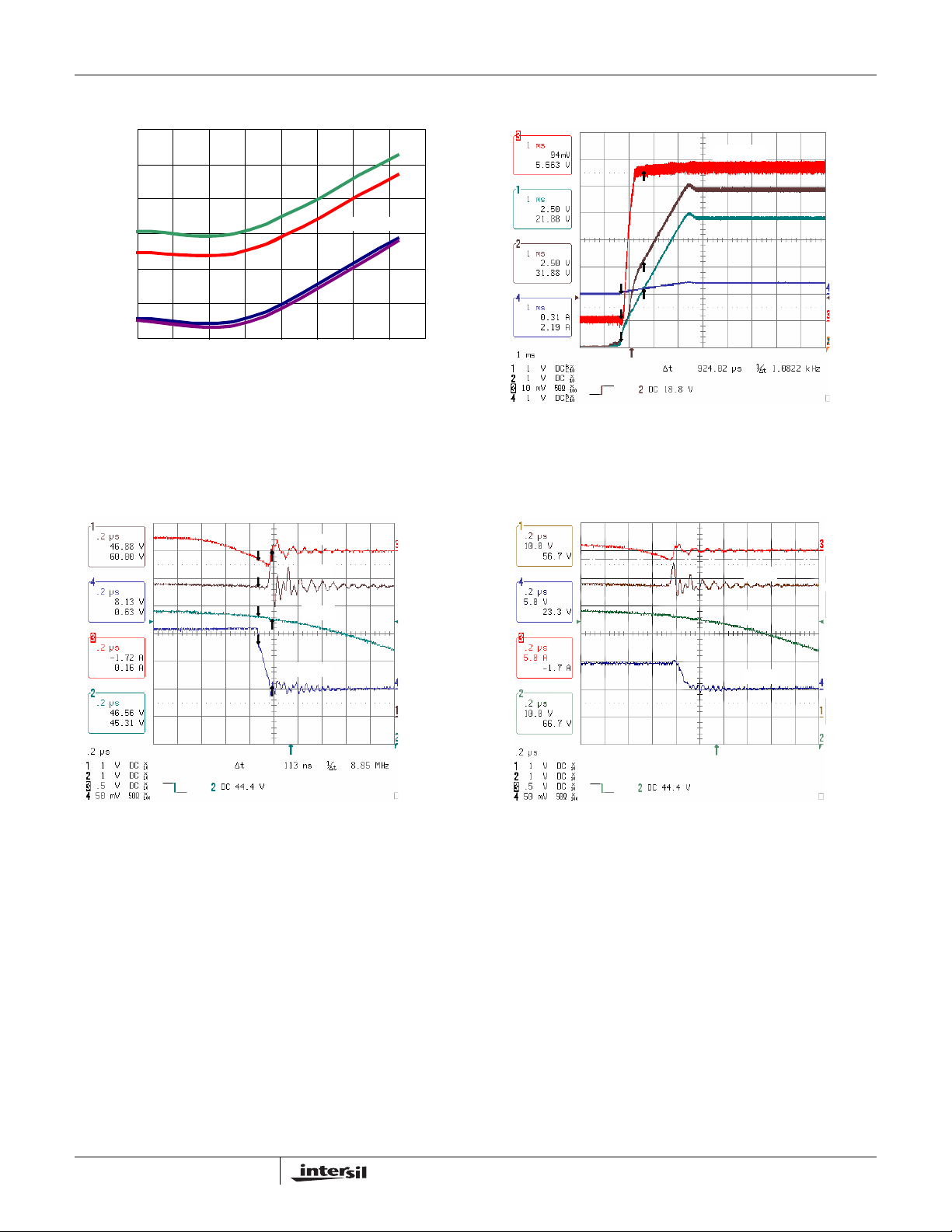
FIGURE 11. HIGH SPEED TURN-OFF, V
LOAD IS SMPS (C
= 100µF) WITH
LOAD
= 48V , COMMON
IN
FIGURE 12. HIGH SPEED TURN-OFF, V
EQUIVALENT 4A LOAD
11
LOAD IS SMPS (C
EQUIVALENT 1.3A LOAD
LOAD
= 48V , COMMON
IN
= 100µF) WITH
February 15, 2007
FN9131.3
Page 12

Typical Performance Curves and Waveforms (Continued)
www.BDTIC.com/Intersil
I
V
OUT
IN2
V
IN2
2A/DIV
10V/DIV
10V/DIV
V
OUT
2V/DIV
V
IN2
V
GS2
V
GS2
FIGURE 13. SLOW SPEED TURN-OFF , VIN = 48V , COMMON
LOAD IS SMPS (C
= 100µF) WITH
LOAD
EQUIVALENT 4A LOAD
Application Circuit
C
1nF
cs1
DC/DC
#1
+IN
PC
PR
-IN
+OUT
+S
SC
-OUT
-S
+OUT1 = 48V
R
Sa
pb1
Sb
10
FROM
CB
INPUT BUS 1
36V TO 75VDC
C
IN1
100µF
220nF
C
d1
5V/DIV
C
pb1
22µF
F1
15A
C
150nF
I
IN2
FIGURE 14. SLOW SPEED TURN-OFF , V
LOAD IS SMPS (C
EQUIVALENT 4A LOAD
D1 (NOTE 7)
Q
1
FDB3632
GATE
1
5V
R
4.99k
3
VIN
HVREF
FAULT
U1
ISL6144
GND
VOUT
COMP
VSET
R
499
R
47.5k
5V/DIV
2A/DIV
= 12V , COMMON
IN
= 100µF) WITH
LOAD
C
2
1
10nF
2
COMMON BUS “CB”
10A
INPUT BUS 2
36V TO 75VDC
C
IN2
100µF
C
220nF
d2
C
PRIMARY
cs2
1nF
DC/DC
#2
+IN
PC
PR
-IN
+OUT
+S
SC
-OUT
-S
+OUT2 = 48V
R
Sa
pb2
Sb
10
FROM
CB
F2
15A
C
pb2
22µF
C
150nF
5V
SECONDARY
3
4.99k
R
4
D2 (NOTE 7)
Q
2
FDB3632
VIN
HVREF
FAULT
GATE
U1
ISL6144
GND
VOUT
COMP
VSET
R
5
499
R
6
47.5k
C
4
10nF
NOTES:
, D2 are parasitic MOSFET diodes.
11. D
1
12. Remote Sense pin (+S) on both DC/DC converters has to be connected either directly at the module output (Sa closed) or to the CB point (Sb
closed). Connecting to CB is not recommended as it might cause Fault propagation in case of short circuit on a PS output.
13. F1, F2 are optional and can be eliminated depending on power system configuration and requirements.
14. DC/DC #1, 2 configuration is based on Vicor V48B48C250AN3.
FIGURE 15. APPLICATION CIRCUIT FOR A 1 + 1 REDUNDANT 48V SYSTEM
12
FN9131.3
February 15, 2007
Page 13

ISL6144
www.BDTIC.com/Intersil
Using the ISL6144EVAL1 High Voltage
ORing MOSFET Controller Evaluation
Board
In a multiple supply, fault tolerant, redundant power
distribution system, paralleled power supplies contribute
equally to the load current through various power sharing
schemes. Regardless of the scheme, a common design
practice is to include discrete ORing power diodes to protect
against reverse current flow should one of the power
supplies develop a catastrophic output short to ground. In
addition, reverse current can occur if the current sharing
scheme fails and an individual power supply voltage falls
significantly below the others.
Although the discrete ORing diode solution has been used
for some time and is inexpensive to implement, it has some
drawbacks. The primary downside is the increased power
dissipation loss in the ORing diodes as power requirements
for systems increase. In some systems this lack of efficiency
results in a cost that surpasses the cost of the ISL6144 and
power FET implementation. The power loss across a typical
ORing diode with 20A is about 10W. Many diodes will be
paralleled to help distribute the heat. In comparison, a FET
with 5mΩ on-resistance dissipates 2W, which constitutes an
80% reduction. When multiplied by the number of paralleled
supplies, the power savings are significant. Another
disadvantage when using an ORing diode would be failure to
detect a shorted or open ORing diode, jeopardizing power
system reliability. An open diode reduces the system to a
single point of failure while a diode short might pose a
hazard to technical personnel servicing the system while
unaware of this failure.
The ISL6144 ORing MOSFET Controller and a suitably
sized N-Channel power MOSFET(s) increase power
distribution efficiency and availability when replacing a
power ORing diode in high current applications. It can be
used in +10V to +75V systems and has an internal charge
pump to provide a floating gate drive for the N-Channel
ORing MOSFET.
The input/output differential trip point “V
programmed by two external resistors (R
This trip point can be adjusted to avoid false gate trip off due
to power supply noise.
The high speed comparator action protects the common bus
from being affected due to individual power supply shorts by
turning off the ORing MOSFET of the shorted feed in less
than 300ns (when using an ORing MOSFET with equivalent
gate to source capacitance equal to 39nF).
- VIN” can be
OUT
, R2 or R6, R7).
1
A circuit fault condition is indicated on an open drain FAULT
pin. The fault detection circuitry covers different types of
failures; including dead short in the sourcing supply, a deadshort of any two ORing MOSFET terminals, or a blown fuse
in the power distribution path.
Typical Application
1
2
VIN1
10V TO 75V
C5*
V
PU
R
3
LED1
RED
VIN2
10V TO 75V
C7*
V
PU
R
4
LED2
RED
VIN
C1
HVREF
FAULT
VIN
C
3
HVREF
FAULT
PS_1
DC/DC
CS
PS_2
DC/DC
= R6 = 499Ω (5%)
R
1
= R7 = 47.5kΩ (5%)
R
2
= R4 = 1.21kΩ (5%)
R
3
= C2 = 150nF (10V)
C
1
= C4 = 10nF (10V)
C
3
C
* TO C8* = 100nF *(100V) Optional Decoupling Caps
5
- LED1, LED2 are red LEDs to indicate a fault, different interfaces
are possible to the FAULT pin.
- VPU is an external pull up voltage source. Also, V
used as the pull up source. In this case if it is higher than 16V,
use a zener diode from the FAULT
voltage less than the rating of the FAULT
Q
1
C6*
GATE
VOUT
U1
ISL6144
COMP
VSET
GND
Q
1
GATE
VOUT
U2
ISL6144
COMP
VSET
GND
pin to GND with a clamping
pin which is 16V.
R
6
OUT
C
2R1
R
2
C8*
R
7
can be
C
4
VOUT
COMMON BUS
Related Literature
• TB389 (PCB Land Pattern Design and Surface Mount
Guidelines for QFN (MLFP) Packages)
• Manufacturer’s MOSFET data sheets
The Hysteretic Regulating (HR) Amplifier provides a slow
turn-off of the ORing MOSFET. This turn-off is achieved in
less than 100μs when one of the sourcing power supplies is
shutdown slowly for system diagnostics, ensuring zero
reverse current. This slow turn-off mechanism also reacts to
output voltage droop, degradation, or power-down.
13
FN9131.3
February 15, 2007
Page 14

ISL6144
www.BDTIC.com/Intersil
DC/DC CONVERTERS (NOT PART OF THE EVAL BOARD) ISL6144EVAL1 CONTROL BOARD
FIGURE 16. TEST SETUP USING DC/DC MODULES
ISL6144 Evaluation Board Overview
This section of the datasheet serves as an instruction
manual for the ISL6144EVAL1 board. It also provides design
guidelines and recommendations for using the ISL6144 for
ORing MOSFET control. The ISL6144EVAL1 Control Board
has two parallel feeds connected to each other through
N-channel ORing MOSFETs. Each ORing MOSFET has an
ISL6144 connected to it. This board demonstrates the
operation of Intersil’s ISL6144 HV ORing MOSFET
Controller IC in a typical 1 + 1 redundant power system.
To demonstrate the functionality of the ISL6144, two power
supplies with identical output voltages are required as the
input to the ISL6144EVAL1 board. This will show the ability
of the ISL6144 to provide the gate drive voltage for the
ORing N-Channel MOSFET. The ISL6144 also monitors the
drain (V
provide reverse current protection and protection against
power feeds’ related faults.
Figure 17 shows a test setup used in the characterization of
ISL6144 in a 1 + 1 redundant power system.
ISL6144EVAL1 Control Board (Rev C)
This board is configured with two input power feeds
connected in parallel for redundancy using ORing
MOSFETs. The ISL6144 allows the two rails to operate in
active ORing mode (This means that both feeds can share
the current if their respective voltages are close to each
), source (VIN) and gate voltages in order to
OUT
other). ORing MOSFET’s gate drive voltage, control and
monitoring for each of these feeds are implemented using
the ISL6144.
The board has the following features:
• Evaluation of the ISL6144 in a 1 + 1 redundant power
system using a single board
• Has footprint for a total of three parallel MOSFETs per
feed. Number of MOSFETs used will depend on the load
current (on the standard ISL6144EVAL1 board only one
MOSFET is populated per feed)
• Allows the user to test turn-on, slow turn-off, fast turn-off
and different fault scenarios
• Visual fault indication with Red LEDs
• Banana Connectors and test points for all inputs, outputs
and IC pins
• Can be easily connected to the power system prototype
for initial evaluation
Note that the board was designed to handle high load
currents (up to 20A per feed) with the appropriate MOSFET
selection.
14
FN9131.3
February 15, 2007
Page 15
ISL6144
www.BDTIC.com/Intersil
Input Voltage Range (+10V to +75V)
The ISL6144 can operate in equipment with voltages in the
+10V to +75V range. The ISL6144 can also be used in
systems with negative voltages -10V to -75V, but it has to be
placed on the return (high) side. For example, in ATCA
systems, an ORing of both the low (-48V) and high (-48V
Return) sides is required. In this case the ISL6144 can be
used on the high side.
The ISL6144 draws bias from both the input and output
sides. External bias voltage rail is not needed and cannot be
used. As soon as the Input voltage reaches the minimum
operational voltage, the internal charge pump turns on and
provides gate voltage to turn-on the ORing FET.
Multiple Feed ORing (ISL6144EVAL1)
In today’s high availability systems, two or more power
supplies can be paralleled to provide redundancy and fault
tolerance. These paralleled power supplies operate in an
active ORing mode where all of these supplies share the
load current, depending on the redundancy scheme
implemented in the particular system. The power system
must be able to continue its normal operation, even in the
event of one or more failures of these power supplies. Faults
occurring on the power supply side need to be isolated from
the common bus point connected to the system critical
loads. This fault isolation device is known as the ORing
device. The function of the ORing device is to pass the
forward supply current flowing from the power supply side
and block the reverse fault current. A fault current might flow
if a short occurs on the input side (typically this could be a
power supply output capacitor short). In this case, the input
voltage drops and current may fl ow in th e reverse direction
from the load to the input, causing the common bus to drop
and the system to fail. Although ORing diodes are simple to
implement in such systems, they suffer from many
drawbacks, as outlined earlier.
The ISL6144 (with an external N-Channel MOSFET)
provides an integrated solution to perform the ORing
function in high availability systems, while increasing power
system efficiency at the same time.
Operating Instructions and Functional
Tests
Test setup for ISL6144EVAL1 is shown in Figures 17 and 18
with two options for the input power sources.
Option 1: Using two identical bench power supplies (BPS)
connected directly to the ISL6144EVAL1 Control Board
(refer to Figure 18). Just make sure to program the voltages
on PS1_V1 and PS2_V2 to identical values so that they
share the load current. A MOSFET (Q
the Input of one or both feeds as close as possible to the
input connectors of the ISL6144EVAL1 board. Slow turn-off
of the input BPS can be performed by the on/off button
) is connected at
short
(depending on the output capacitance value of the power
supply/module, a local loading resistor might be needed to
help discharge the BPS output capacitor). An output
capacitor C
(equivalent to the capacitor that will be used
OUT
in the final power system solution) is connected to the
Common Bus point (V
). Different types of loads can be
OUT
used (power resistors, electronic load or simply another
DC/DC converter).
AUX PS*
+
-
5V
+
PS1
+48V
-
+
PS2
+48V
BENCH POWER
SUPPLIES
* Auxiliary power supply is used to power the LED circuit. If V
less than 16V , J1 can be connected directly to V
higher than 16V, we still can use V
zener diode has to be connected from FAULT
voltage across the pin to 16V or lower.
FIGURE 17. TEST SETUP USING BENCH PS
USED ONL Y FOR POWERING THE LEDS
PS1_V1 = V
PS1_V1RTN
PS2_V2 = V
PS2_V2RTN
IN1
IN2
Q
SHORT
J4
V
IN1
J6
GND
V
IN2
J8
GND
ISL6144EVAL1
to replace AUX PS, but a
OUT
J1
5V_AUX
J2
C
OUT
J3
GND
(J5). If V
OUT
V
J7
CONTROL
BOARD
OUT
to GND to clamp the
OUT
OUT
L
O
A
D
is
is
Option 2: Using a custom designed DC/DC converter Power
Board which consists of two DC/DC modules connected in
current sharing configuration, each DC/DC module output
can be turned off slowly using the ON/OFF pin or can be
shorted using on-board Power MOSFET (Refer to
Figure 19). In this case also, similar considerations for C
OUT
and type of load apply as in option 1 above.
+
AUX PS
-
+
PS1
+48V
-
+
PS2
+48V
-
BENCH POWER
SUPPLIES
* Power Modules Board can be replaced by bench power supplies or
any discrete DC/DC modules. Just make sure to adjust both V
and V
OUT2
two modules (Refer to option 1 and Figure18).
FIGURE 18. TEST SETUP USING DC/DC MODULES
USED ONLY FOR POWERING THE LEDs
PS1_V1
PS1_V1RTN
PS2_V2
PS2_V2RTN
J1
V
OUT1
DC/DC 1
J2
PRI_GND
J3
J9
PRI_GND
POWER MODULES CONTROL
CS
V
OUT2
DC/DC 2
GND
GND
J4
J6
J7
J8
J4
J1
5V_AUX
V
IN1
J6
GND
J7
V
J8
GND
ISL6144EVA L1
IN2
V
OUT
GND
BOARDBOARD*
J2
C
OUT
J3
OUT1
close to each other to allow current sharing between the
L
O
A
D
15
FN9131.3
February 15, 2007
Page 16

ISL6144
www.BDTIC.com/Intersil
DC/DC Converter Power Board (not part of the
ISL6144EVAL1 board)
The DC/DC converter board consists of two DC/DC
converters with independent input voltage rails. In reality, two
identical power supplies can be used in the test setup to
replace this board (Contact Intersil Applications Engineering
if you need assistance in your test setup). This DC/DC
converter board is configured for operation at different output
voltage levels depending on the choice of DC/DC modules.
Most evaluation results are provided for a mix of +48V and
+12V input voltages. Any other voltage within the +10V to
+75V range can also be used.
Each DC/DC converter has a low r
DS(ON)
MOSFET
connected in parallel to the output terminals. This MOSFET
is normally off. When turned on it simulates a short across
the output. Another MOSFET is connected at the ON/OFF
pin of the modules to simulate a slow turn-off of the module.
Single Feed Evaluation
The ISL6144EVAL1 is hooked up to two input power
supplies using test setup shown in Figure 18 or Figure 19.
Note that the ISL6144EVAL1 is populated with one
FDB3632 MOSFET per feed (Nominal value of the
MOSFET’s r
1. Connect the input power supplies, auxiliary 5V power
supply, load and output capacitor to the ISL6144EVAL1.
2. Connect test equipment (Oscilloscope, DMM) to the
signals of interest using on-board test points and scope
probe jacks.
3. Turn-on PS1 with V
within +10V to +75V). Turn-on the auxiliary power supply
(AUX PS powering the LED circuit) with +5V . Adjust load
current to 2A. Verify the main operational parameters
such as the 20mV forward regulation at light loads, and
gate voltage as a function of load current.
4. The forward voltage drop across the MOSFET terminals
(TP1-TP2) is equal to the maximum of the 20mV
V
SD1
forward regulated voltage drop across the source-drain
“V
FWD_HR
MOSFET on-state resistance “I
5. For I
Load
gate-source voltage is modulated as a function of load
current and MOSFET transconductance. Gate-source
voltage V
case, LED1 is off. LED2 will be RED as V
6. Increase the load current I
increased to above V
forward regulation cannot be maintained. The MOSFET
cannot deliver the required load current with a 20mV
constant V
pumped to V
7. Turn-off V
listed above. Make sure the ISL6144 is providing gate
voltage, which is modulated based on the load current.
is measured between (TP4-TP5), V
V
SD2
measured between (TP14-TP21).
is approximately 8mΩ at VGS=10V).
DS(ON)
= +48V (V
IN1
can be any voltage
IN1
“ or the product of the load current and the
* r
Load
= 2A, V
(TP13 -TP17) is approximately 4V. In this
GS1
SD1
GQP
and turn-on V
IN1
is equal to V
SD1
Load
FWD_HR
FWD_HR
to 4A. Note that V
and operation in the 20mV
. In this case, gate voltage is fully charge-
(10.6V nominal).
and repeat the same tests
IN2
”.
DS(ON)
= 20mV . The
is still off.
IN2
is
GS2
DS1
is
Two Feed Parallel Evaluation
Two Feed parallel operation verification can be performed
after completion of the single feed evaluations. Make sure
that the two Input power supplies connected to the
ISL6144EVAL1 board are identical in voltage value. Identical
input voltages are needed to enable the two feeds to share
the load current (In real world power systems, current
sharing is most likely insured by the power supplies/modules
that have an active current sharing feature).
1. Turn-on PS1 and PS2 in sequence (hot plugging is not
recommended). Adjust V
IN1
and V
close to each
IN2
other. Verify the input current of both feeds to be within
acceptable current sharing accuracy (~10%). Current
sharing accuracy will be very poor at light loads and
becomes better with higher load currents.
2. Adjust the load current to different values and verify that
both V
(TP1 to TP2) and V
SD1
(TP4 to TP5) are close
SD2
to each other. These two voltages might be different
depending on the amount of load current passing through
each of the two feeds.
3. At light loads, I
Load
* r
is less than 20mV, the
DS(ON)
ISL6144 operates in the forward regulation mode and
gate voltage is modulated as a function of load current.
When I
Load*rDS(ON)
becomes higher than the regulated
20mV, the charge pump increases and clamps the gate
voltage to the maximum possible charge pump voltage,
.
V
GQP
4. Verify the Gate voltage of both MOSFETs V
TP17) and V
(TP14 to TP21) with different load
GS2
GS1
(TP13 to
currents.
5. Both LED1 and LED2 are off when both feeds are on.
6. For I
turned off. LED2 is RED and V
around 4V to V
7. Turn V
LED1 is RED. V
= 4A, turn-off V
Load
GQP
back on and turn V
IN2
GS2
and note that V
IN2
has increased from
GS1
.
off. V
IN1
has increased to V
is now off.
GS1
.
GQP
GS2
has
Performance Tests
Performance tests can be carried out after the two feeds
have been verified and found to be operational in active,
1 + 1 redundancy (when two feeds share the load current,
current sharing is ensured by the incoming power supplies.)
These include gate turn-on at power supply start-up, fast
speed turn-off (in case of fast dropping input rail), slow
speed turn-off (in response to slow dropping input rail) and
fault detection in response to different faults.
Gate Start-Up Test
FIRST FEED START-UP
When the first feed is turned on, as V
occurs through the body diode of the MOSFET. This only
occurs for a short time until the MOSFET gate voltage can
be charge-pumped on. This conduction is necessary for
proper operation of the ISL6144. It provides bias for the gate
hold off and other internal bias and reference circuitry. The
rises, conduction
IN1
16
FN9131.3
February 15, 2007
Page 17

ISL6144
www.BDTIC.com/Intersil
charge pump circuitry starts functioning as the input voltage
at the V
pin reaches a value around 8V. The gate voltage
IN
depends on the load current (as explained in previous
sections), The maximum gate voltage will be clamped to a
maximum of V
when load current becomes too high to
GQP
be handled with 20mV across the source-drain terminals.
Overall, it takes less than 1ms to reach the load-dependant
final gate voltage value. Note that the Input voltage cannot
be hot swapped and has to rise slowly. A rise time of at least
one ms is recommended for the voltage at VIN pin.
V
= 48V; RESISTIVE LOAD = 4A, C
IN
V
IN1,VG1,IIN1
HV
REF(Vz)
5V/DIV
0A
, VG1, I
VIN1
0A
and HV
REF(VZ)
I
IN1
2A/DIV
V
10V/DIV
WHEN VIN REACHES ~ 8V AND HVREF REACHES
3V to 4V, GATE CHARGE PUMP ACTION STARTS
and V
IN1
I
5A/DIV
V
OUT
20V/DIV
OUT
IN1
WAVEFORMS
G1
WAVEFORMS
GSEXT
V
IN1
10V/DIV
= 33nF
4A
4A
V
= 12V; RESISTIVE LOAD = 5A, C
IN
5A/DIV
V
5V/DIV
FIGURE 20. FIRST FEED V
I
IN1
IN1
V
OUT
5V/DIV
START-UP (12V CASE)
IN1
GSEXT
5V/DIV
V
G1
= 33nF
The start-up tests were done with the addition of an external
gate to source capacitor to demonstrate start-up time with a
total equivalent gate-source capacitance around 39nF.
SECOND (CONSECUTIVE) FEED START-UP
In this case, the ISL6144 for the second (consecutive) feed
(U4) already has output bias voltage as the first parallel feed
has been turned on and V
bus. As V
rises, VG2 rises with it (V
IN2
with respect to GND). When V
is present on the common
OUT
approaches V
IN2
is GATE2 voltage
G2
IN1
value,
Gate 2 is turned. Second feed gate turn-on is faster than the
first feed as the HVREF capacitor (C
) is already
3
charged.The second or consecutive power supply to be
started can be turned on faster than the first power supply, a
rise time of at least 200µs of the second rail is
recommended.
V
= 48V; RESISTIVE LOAD = 4A, C
IN
GS(EXT)
= 33nF
V
G1
20V/DIV
WHEN VIN REACHES ~ 8V
AND HVREF REACHES 3V TO 4V
GATE CHARGE PUMP ACTION STARTS
FIGURE 19. FIRST FEED V
START-UP (48V CASE)
IN1
V
IN1
20V/DIV
SECOND GATE TURNS ON ONLY
WHEN V
POWER SUPPLY
RELATED DELAY
FIGURE 21. SECOND (CONSECUTIVE) FEED V
17
I
IN2
2A/DIV
IN THIS CASE GATE VOLTAGE IS MEASURED
BETWEEN GATE2 AND GND
REACHES V
IN2
IN1
20V/DIV
V
G2
V
IN2
20V/DIV
V
OUT
20V/DIV
IN2
START-UP
FN9131.3
February 15, 2007
Page 18
ISL6144
www.BDTIC.com/Intersil
Gate Fast Turn-off Test
During normal operation, the ISL6144 provides gate drive
voltage for the ORing MOSFET when the Input voltage
exceeds the output voltage. The current flows in the forward
direction from the input to the output. Now, what happens if
the input voltage drops quickly below the output voltage as a
result of a failure on the input sourcing power supply while
the MOSFET remained on? The answer is: If the MOSFET is
kept on, current starts to flow in the reverse direction from
the output to the input. Of course this is not desired nor
acceptable. It will lead to effectively shorting the output and
causing an overall system failure. In order to block this
reverse current, the ISL6144 senses the voltage at both VIN
and COMP pins (this is V
programmable threshold (V
55mV on the EVAL board and could be adjusted by
changing R
COMP (V
, R4 values for both feeds. If VIN drops below
1
- V
OUT
TH(HS
off the gate of the ORing MOSFET very quickly, the gate pull
down current I
is 2A. As a result the reverse current flow
PDH
is prevented. The maximum turn-off time is less than 300ns
when using an ORing MOSFET(s) with an equivalent gatesource capacitance of 39nF (equivalent to Q
V
= 10V).
GS
On the ISL6144EVAL1 board, FDB3632 has an equivalent
gate-source capacitance of 8.4nF, some of the tests are
performed while an external gate to source capacitance is
added to demonstrate gate current sink capability.
voltage reduced by a resistor
OUT
), it is programmed to
TH(HS
), the High Speed Comparator turns
= 390nC at
TOT
t
DELAY(HS)
is the High Speed Comparator internal worstcase time delay. The setup in Figure 18 can be used to
perform the Input dead-short test; a pulse generator is
connected between Gate-Source of Q
SHORT1
(use pulse
mode single shot, set the frequency to <10Hz and pulse
width of approximately 10ms, t
= 1µs). Follow steps
RISE
1 through 5 in the two feed parallel operation section. Make
sure that both feeds operate in parallel current sharing
mode. Proceed with the short test by applying the single
pulse to the gate of Q
shorts V
causing it to fall quickly (in less than 10µs).
IN1
SHORT1
. Once turned on, Q
SHORT1
Figures 23, 24 and 25 show the results for different
combinations of C
connect the V
IN1
possible to the V
and load current. Make sure to
GS1
shorting-MOSFET terminals as close as
-GND (J4 to J6) terminals on the EVAL
IN
board to minimize lead impedance and reduce parasitic
ringing.
V
= V
IN2
gs(ext)
V
OUT
10V/DIV
= 48V;
= 33nF
I
IN1
2A/DIV
REVERSE CURRENT
V
GS1
5V/DIV
V
IN1
10V/DIV
IN1
RESISTIVE LOAD = 6A, C
V
= V
IN1
FIGURE 22. FAST SPEED TURN-OFF
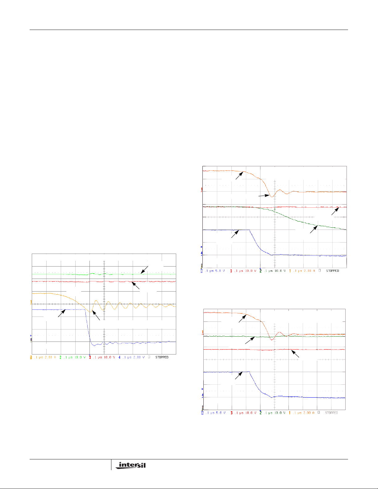
= 48V; RESISTIVE LOAD = 4A, C
IN2
I
IN1
2A/DIV
V
GS1
2V/DIV
0.1µs/DIV
(MOSFET WITH Q
GS(EXT)
REVERSE CURRENT DISSAPPEARS
WHEN GATE IS COMPLETELY OFF
= 8.4nc)
TOT
Worst-case turn-off time can be calculated as:
V
⎛⎞
GS
-------------
t
toff WC()tDELAY HS()CGS
t
toff WC()
50ns 39nF
+=
⎜⎟
I
⎝⎠
PDH
12V
⎛⎞
---------- -
2A
284ns=+=
⎝⎠
= 0nF
V
OUT
10V/DIV
V
G2
10V/DIV
(EQ. 9)
0.1µs/DIV
FIGURE 23. FAST SPEED TURN-OFF (MOSFET WITH
= 8.4nc) AND 33nF EXTERNAL C
Q
TOT
V
= V
IN1
I
IN1
2A/DIV
V
G2
10V/DIV
V
GS1
5V/DIV
0.1µs/DIV
FIGURE 24. FAST SPEED TURN-OFF (MOSFET WITH
Q
TOT
RESISTIVE LOAD = 6A, C
V
10V/DIV
= 8.4nc) AND 33nF EXTERNAL C
IN2
gs(ext)
OUT
GS
= 48V;
= 33nF
gs
18
FN9131.3
February 15, 2007
Page 19

ISL6144
www.BDTIC.com/Intersil
The ISL6144EVAL1 board has V
of 55mV. It can be
TH(HS)
changed if performance is found to be unacceptable with this
value. V
can affect the amplitude of the reverse current
TH(HS)
(short pulse) that might flow before the gate is effectively
turned off (details on how to select V
later section of this application note). The r
is included in a
TH(HS)
DS(ON)
and internal
HS comp offset also contribute to the amplitude of the reverse
current pulse. A short event on a single feed may cause
ringing on the ground pins, the V
, and on the V
IN
OUT
pins.
This ringing may cause false turn-off on the healthy feeds.
Using decoupling capacitors both at the V
and V
IN
OUT
pins
help in filtering this high frequency ringing and prevent false
turn-off of parallel feeds. Figure 25 shows th at the gate of
second feed V
(measured with respect to ground) is not
G2
affected when feed 1 input is shorted.
Power Supply Slow Turn-off
In many cases, a single power feed is turned off for
diagnosis, maintenance or replacement. The Input voltage
drops slowly (most probably in few ms). When voltage at V
pin starts dropping with respect to V
Regulating Amplifier starts pulling down current (I
pin. The Hysteretic
OUT
PDL
opposite to the charge pump current. This reduces the gate
voltage gradually until the MOSFET is completely turned off.
The slow turn-off is accomplished with zero reverse current.
An internal 20μs delay filters out any false trip off due to
noise or glitches that might be present on the supply line.
IN
)
Input Voltage is falling at a slow rate (Figure 26, top scope
shot shows a 20ms fall time for the input voltage).
V
(Common Bus) remains almost unchanged at around
OUT
48V. It drops by a value equivalent to the increase in the
portion of the load current passing through the remaining
feed multiplied by the MOSFET’s r
DS(ON)
.
At the beginning of the slow turn-off, the gate drive Voltage
V
(measured between the Gate and Source of the
GS1
ORing MOSFET using a differential probe) starts to drop at a
slower rate. This is attributed to the effect of the 20µs
filtering-delay. Afterwards a stronger pul l down curre nt st art s
and finally the high-speed turn-off completes the gate turnoff. Current through the turned off feed is also shown to be
positive and the turn-off is complete with no reverse current.
Figure 26 shows the same slow turn-off for a 12V input
voltage case.
= V
IN2
= 12V
V
IN1
The slow speed turn-off mechanism is shown in Figure 25:
= V
IN2
= 48V
V
IN2
V
IN2
10V/DIV
V
OUT
10V/DIV
I
IN2
2A/DIV
5V/DIV
V
GS2
I
IN2
V
OUT
V
5ms/DIV
V
IN1
GS2
ZOOMED IN VIEW
5ms/DIV
ZOOMED IN VIEW
V
GS1 (DIFF PROBE)
5V/DIV
20µs/DIV
FIGURE 26. SLOW SPEED TURN-OFF (C
GSTOT
V
OUT
2V/DIV
V
IN1
2V/DIV
I
IN1
2A/DIV
= 8.4nF + 33nF)
20µs/DIV
FIGURE 25. SLOW SPEED TURN-OFF (C
GSTOT
= 8.4nF + 33nF)
19
FN9131.3
February 15, 2007
Page 20

ISL6144
www.BDTIC.com/Intersil
Detection of Power Feed Faults
The ISL6144 have two built-in mechanisms that monitor
voltages at VIN, VOUT and GATE pins. The first mechanism
monitors GATE with respect to VIN (with a 410mV threshold)
and the second mechanism monitors V
VOUT (with 370mV threshold). The open-drain FAULT
will be pulled low when any of the two above conditions is
met.
Some of the typical system faults detected by the ISL6144
are:
Fault 1: Open Fuse at the Input Side
(Fuse has to be placed before the VIN tap, between the
power supply and the source of the ORing MOSFET), note
that the EVAL board does not have footprint for installing this
fuse. This feature can be tested by adding a fuse externally.
The open fuse results in near zero current flow through the
ORing MOSFET, only a very low current drawn by the IC
bias will flow. The voltage at VIN pin is effectively
disconnected from the power source and will start dropping
slowly. The regulated source-drain voltage falls below its
20mV level and the gate of the MOSFET is pulled down and
turned off. GA TE will become low and a fault is indicated with
internal built in delay (t
FLT
).
Fault 2: Drain to Source Short
In this case VIN is shorted to V
drop across the shorted MOSFET terminals will be close to
0V. The Gate will be pulled down and a fault will be
indicated. The resistance of the Drain to Source short
multiplied by the Drain short current must be low enough to
result in V
SD
< V
FWD_HR
values), Otherwise this fault cannot be detected.
V
= 12V, FAULT PULLED TO +5V
IN
V
G1
5V/DIV
OUT
(refer to data sheet for worst case
V
OUT
5V/DIV
with respect to
IN
pin
, and in theory the voltage
FAULT
5V/DIV
V
IN1
5V/DIV
Fault 3: MOSFET Gate to Source Dead Short
GA TE voltage will be equal to VIN, GA TE <V
fault is indicated.
V
= 12V, FAULT PULLED TO +5V
IN
FAULT
V
OUT
5V/DIV
5V/DIV
V
G1
5V/DIV
TIME SCALE
100µs/DIV
FIGURE 28. MOSFET GATE TO SOURCE FAULT
+ 0.37V and a
IN
V
IN1
5V/DIV
Fault 4: ORing FET Off Condition
When VIN < V
flow. This means that if an ORing feed is not sharing current,
a fault will be indicated. Also if a feed (PS) is off while bias is
applied from V
, the Gate is off to block reverse current
OUT
to that feed, then a fault is also indicated.
OUT
Fault 5: MOSFET Gate to Drain Dead Short
In this case, the following condition will be violated GATE
<V
+ 0.37V and a fault is issued.
IN
V
= 12V, FAULT PULLED T O +5V
IN
FAULT
V
OUT
5V/DIV
5V/DIV
V
IN1
5V/DIV
V
G1
5V/DIV
TIME SCALE
TIME SCALE
100µs/DIV
FIGURE 27. MOSFET DRAIN TO SOURCE FAULT
100µs/DIV
FIGURE 29. MOSFET GATE TO DRAIN FAULT
20
FN9131.3
February 15, 2007
Page 21

ISL6144
www.BDTIC.com/Intersil
Fault 6: ORing FET Body Diode Conduction
(V
- 0.41V > V
IN
). If the voltage drop across the
OUT
MOSFET approaches 410mV, a fault will be indicated. Make
sure the selection of the ORing MOSFET takes this fact into
account.
Application Considerations and
Component Selection
“ISL6144 + ORing FET” vs “ORing Diode” Solution
“ISL6144 + ORing FET“ solution is more efficient than the
“ORing Diode” Solution, which will result in simplified PCB
and thermal design. It will also eliminate the need for a heat
sink for the ORing diode. This will result in cost savings. In
addition is the fact that the ISL6144 solution provides a more
flexible, reliable and controllable ORing functionality and
protects against system fault scenarios (Refer to the fault
detection block description.)
On the other hand the most common failures caused by
diode ORing include open circuit and short circuit failures. If
one of these diodes (Feed A) has failed open, then the other
Feed B will provide all of the power demand. The system will
continue to operate without any notification of this failure,
reducing the system to a single point of failure. A much more
dangerous failure is where the diode has failed short. The
system will continue to operate without notification that the
short has occurred. With this failure, transients and failures
on Feed B propagate to Feed A. Also, this silent short failure
could pose a significant safety hazard for technical
personnel servicing these feeds.
“ISL6144 + ORing FET” vs “Discrete ORing FET”
Solution
If we compare the ISL6144 integrated solution to discrete
ORing MOSFET solutions (with similar performance
parameters), the ISL6144 wins in all aspects, the main ones
being simplicity of an integrated solution, PCB real estate
saving, cost savings, and reduction in the MTBF of this section
of the circuit as the overall number of components is reduced.
For example, in a 48V , 32A (1 + 1) redundant system with
current sharing, using a Schottky diode as the ORing device
(Refer to Figure 31), the forward voltage drop is in the
0.4V to 0.7V range, (let us assume it is 0.5V). The power loss
across each diode is shown in Equation 10:
I
OUT
P
loss D1()Ploss D2()
---------------
VF⋅ 16A 0.5V⋅ 8W====
2
(EQ. 10)
The total power loss across the two ORing diodes is 16W.
D
1
INPUT BUS 1
INPUT BUS 2
FIGURE 30. 1 + 1 REDUNDANT SYSTEM WITH DIODE ORING
DC/DC
CS
DC/DC
+IN1 = 48V
1
+IN2 = 48V
2
0.5V@ 16A
D
2
0.5V @ 16A
V
OUT
(32A)
If we use a 4.5mΩ MOSFET (refer to Figure 32), the nominal
Power loss across each MOSFET is:
2
I
OUT
⎛⎞
P
P
loss
loss
P
M1()
NOM M1()
loss M2()
16A()
---------------
⎝⎠
2
4.5mΩ⋅ 1.152W==
2
r
⋅==
DS ON()
(EQ. 11)
The total power loss across the two ORing MOSFETs is
2.304W.
In case of failure of current sharing scheme, or failure of
DC/DC 1, the full load will be supplied by DC/DC 2. ORing
MOSFET M2 or ORing Diode D
will be conducting the full
2
load current. Power lost across the ORing devices are:
P
P
loss
loss
MAX D2()
MAX M2()
I
⋅ 32A 0.5V⋅ 16W===
OUTVF
2
r
I
()
⋅ 32A()24.5mΩ⋅ 4.6W===
OUT
DS ON()
(EQ. 12)
(EQ. 13)
In brief, the solution offered by this IC enhances power
system performance and protection while not adding any
considerable cost, on the contrary saving PCB board real
INPUT BUS 1
estate and providing a simple to implement integrated
solution.
ORing MOSFET Selection
Using an ORing MOSFET instead of an ORing diode results
in increased overall power system efficiency as losses across
the ORing elements are reduced. The benefit of using ORing
MOSFETs becomes even more significant at higher load
currents as power loss and forward voltage drop across the
traditionally used ORing diode is increased. The high power
dissipation across these diodes requires paral leli ng of many
diodes as well as special thermal design precautions such as
heat sinks (heat dissipating pads) and forced airflo w.
21
INPUT BUS 2
FIGURE 31. 1+1 REDUNDANT SYSTEM WITH MOSFET ORING
DC/DC
1
CS
DC/DC
2
+IN1 = 48V
+IN2 = 48V
M1
4.5mΩ
0.072V @ 16A
M2
4.5mΩ
0.072V@ 16A
February 15, 2007
V
OUT
(32A)
FN9131.3
Page 22

ISL6144
www.BDTIC.com/Intersil
This shows that worst-case failure scenario has to be
accounted for when choosing the ORing MOSFET. In both
cases, more than one ORing MOSFET/diode has to be
paralleled on each feed. Using parallel devices reduces
power dissipation per device and limits the junction
temperature rise to acceptable safe levels. Another
alternative is to choose a MOSFET with lower r
DS(ON)
(Refer to Table 1 and Table 2 for some examples).
If parallel MOSFETs are used on each feed, make sure to
use the same part number. Also it is preferable to have parts
from the same lot to insure load sharing between these
paralleled devices.
The final choice of the N-Channel ORing MOSFET depends
on the following aspects:
• Voltage Rating: The drain-source breakdown voltage
V
has to be higher than the maximum input voltage,
DSS
including transients and spikes. Also, the gate to source
voltage rating has to be considered. The ISL6144
maximum Gate charge voltage is 12V . Make sure the used
MOSFET has a maximum V
rating >12V.
GS
• Power Losses: In this application, the ORing MOSFET is
used as a series pass element, which is normally fully
enhanced at high load currents. Switching losses are
negligible. The major losses are conduction losses, which
depend on the value of the on-state resistance of the
MOSFET r
, and the per feed load current. For an
DS(ON)
N + 1 redundant system with perfect current sharing, the
per feed MOSFET losses are:
P
loss FET()
⎛⎞
-----------------
⎝⎠
N1+
r
⋅=
DS ON()
(EQ. 14)
2
I
LOAD
• The final MOSFET selection has to be based on the worse
case current when the system is reduced to N parallel
supplies due to a permanent failure of one unit. The
remaining units have to provide the full load current. In this
case, losses across each remaining ORing MOSFET
become:
2
I
LOAD
⎛⎞
P
loss FET()
-----------------
⎝⎠
r
⋅=
N
DS ON()
(EQ. 15)
Suppose P
ambient thermal resistance R
copper pad area), T
= 1W in a D2PAK MOSFET, junction to
Loss
JMAX
= +175°C, r
= +43°C/W (with 1 inch2
θJA
DS(ON)
= 4.5mΩ,
maximum ambient board temperature = +85°C.
We need to make sure that the MOSFET’s junction
temperature during operation does not exceed the maximum
allowable device junction temperature.
T
= T
J
A_max
+ P
Loss
• R
θJA
TJ = +85°C+1W. +43°C/W = +128°C
TJ < T
JMAX
In the example of Figure 32 with a load of 32A, at least 3
MOSFETs with r
DS(ON)
= 4.5mΩ are paralleled to limit the
dissipation to below 1W and operate with safe junction
temperature.
The following tables show MOSFET selection for some
typical applications with different input voltages and load
currents in a 1 + 1 redundant power system (a maximum of
1W of power dissipation across each MOSFET is assumed).
For a 48V Input:
TABLE 1. INPUT VOLTAGE = 48V
I
Load_Max
8A FDB3632 (Note 8)
16A FDB3632 (Note 8)
32A FDB3632 (Note 8)
NOTES:
7. Number of parallel MOSFETs per feed
8. V
9. V
10. V
= 100V;ID = 80A; r
DSS
= 100V; ID = 110A; r
DSS
= 75V; ID = 80A; r
DSS
MOSFET PART NUMBER N (Note 7)
1
SUM110N10-08 (Note 9)
SUM110N10-08
FDB045AN08A0 (Note 10)
SUM110N10-08
FDB045AN08A0
= 9mΩ
DS(ON)
= 9.5mΩ
DS(ON)
= 4.5mΩ
DS(ON)
1
2
2
1
4
4
3
• In the particular cases illustrated in the previous examples
of Figures 31 and 32 with N = 1, each of the two ORing
feeds have to be able to handle the full load current.
• The MOSFET’s r
DS(ON)
value also depends on junction
temperature; a curve showing this relationship is usually
For a 12V to 24V Input:
TABLE 2. INPUT VOLTAGE = 12V TO 24V
I
Load_Max
15A IRF1503S (Note 11)
part of any MOSFET’s data sheet. The increase in the
value of the r
account.
over-temperature has to be taken into
DS(ON)
40A IRF1503S
• Current handling capability, steady state and peak, are
also two important parameters that must be considered.
The limitation on the maximum allowable drain current
comes from limitation on the maximum allowable device
junction temperature. The thermal board design has to be
able to dissipate the resulting heat without exceeding the
MOSFET’s allowable junction temperature.
NOTES:
11. V
12. V
13. V
14. All Above listed r
= 30V; ID = 190A; r
DSS
= 30V; ID = 110A; r
DSS
= 30V; ID = 100A; r
DSS
22
MOSFET PART NUMBER N
SUM110N03-03P (Note 12)
STB100NF03L-03 (Note 13)
SUM110N03-03P
STB100NF03L-03
= 3.3mΩ
DS(ON)
= 2.6mΩ
DS(ON)
= 3.2mΩ
DS(ON)
DS(ON)
values are at V
GS
= 10V
1
1
1
2
2
2
FN9131.3
February 15, 2007
Page 23

ISL6144
www.BDTIC.com/Intersil
TABLE 2. INPUT VOLTAGE = 12V TO 24V
I
Load_Max
75A IRF1503S
NOTES:
11. V
12. V
13. V
14. All Above listed r
= 30V; ID = 190A; r
DSS
= 30V; ID = 110A; r
DSS
= 30V; ID = 100A; r
DSS
MOSFET PART NUMBER N
SUM110N03-03P
STB100NF03L-03
= 3.3mΩ
DS(ON)
= 2.6mΩ
DS(ON)
= 3.2mΩ
DS(ON)
DS(ON)
values are at V
GS
= 10V
3
3
3
Another important consideration when choosing the ORing
MOSFET is the forward voltage drop across the drainsource. If this drop approaches the 0.41V limit, (which is
used in the V
fault monitoring mechanism), this will
OUT
result in a permanent fault indication. Normally, this voltage
drop is chosen to be less than 100mV.
Setting the External HS Comparator
Threshold Voltage
Typically, DC/DC modules used in redundant power systems
have some form of active current sharing to realize the full
benefit of this scheme including lower operating
temperatures, lower system failure rate, as well as better
transient response when load step is shared. Current
sharing is realized using different techniques; all of these
techniques will lead to similar modules operating under
similar conditions in terms of switching frequency , duty cycle,
output voltage and current. When paralleled modules are
current sharing, their individual output ripple will be similar in
amplitude and frequency and the common bus will have the
same ripple as these individual modules and will not cause
any of the turn-off mechanisms to be activated as the same
ripple will be present on both sensing nodes (V
V
). This would allow setting the high speed comparator
OUT
threshold (V
V
of 55mV could be used, the final value of this TH
TH(HS)
) to a very low value. As a starting point, a
TH(HS)
will be system dependant and has to be finalized in the
system prototype stage. If the gate experiences false turn-off
due to system noise, the V
has to be increased.
TH(HS)
The reverse current peak can be estimated as:
V
TH HS()VSDVOS HS()
I
REVERSEP
V
is the MOSFET forward voltage drop
SD
V
OS(HS)
----------------------------------------------------------------------
is the voltage offset of HS Comparator
±+
r
DS ON()
where;=
The duration of the reverse current pulse is in the order of a
few hundred nanoseconds and is normally kept well below
the current rating of the ORing MOSFET.
IN
and
(EQ. 16)
Just a reminder, this is not an operating scenario, but it is
rather a fault scenario and should not occur frequently. As
explained above, different power supplies have different
noise spectrum and might need adjustment of the V
The following procedure can be used for V
Choose a value of V
such that the net HS comp arator
TH(HS)
TH(HS)
threshold voltage is positive to allow turn-off only when V
TH(HS)
selection:
IN
is lower than COMP. Take into account the worst-case of the
HS Comp offset (V
starting value is 55mV. The sum of R
exceed 50kΩ. It is suggested to choose R
calculate R
=
R
1
R
= 499Ω
1
according to Equation 17:
1
V
---------------------------------------------------------------- -
V
TH HS()
REF VSET()VTH HS()
= +25mV to -40mV). A good
OS(HS)
–
R
2
and R2 is not to
1
= 47.5kΩ and
2
(EQ. 17)
R1 resistor connected between VOUT and COMP pins
R2 resistor connected between COMP and VSET pins
V
REF(VSET)
= 5.3V
1. Operate all parallel feeds in current sharing mode (either
by using current sharing techniques or by simply
adjusting the voltages very close to each other for natural
current sharing).
2. Vary the load current from 1A to its maximum value,
monitor the gate voltages, and make sure all gates are on
(note that at very light loads the current sharing scheme
might stop functioning and only one feed carries this light
current, at this point gate voltages will be just above the
gate threshold, and even maybe one gate will be on while
the others are not).
3. If at medium to maximum load currents all feeds have
their gates on, then the chosen V
TH(HS)
is suitable.
4. If only one feed has its gate on, the threshold value is too
low and the gate is turning off due to power supply noise
and needs to be increased. Also, the feeds may not be
sharing the load current due to discrepancy in output
voltages and current sharing failure.
5. Verify the current sharing scheme and output voltages. If
the output voltages and currents of each feed are equal
but one or more of the gates is still off, increase V
TH(HS)
by increasing R1 in 250Ω to 500Ω increments (this
increases V
by 25mV to 50mV) until all feeds have
TH(HS)
their FETs turned on.
.
Reducing the value of V
results in lower reverse
TH(HS)
current amplitude and reduces transients on the common
bus voltage.
23
FN9131.3
February 15, 2007
Page 24

INCREASE
www.BDTIC.com/Intersil
V
TH(HS)
(BY INCREASING
R1 ONLY)
NO
START
SET V
OPERATE ALL FEEDS IN
CURRENT SHARING MODE
(V
IN1
COMPARE GATE-SOURCE
V
GS1
= 55mV
TH(HS)
R
= 499Ω
1
= 47.5kΩ
R
2
= V
=...= V
IN2
n = N+1
VOLTAGES
≅ V
≅...V
GS2
INn
GSn
)
ISL6144
Q
GATE
ISL6144
GND
GATE
ISL6144
GND
1
VOUT
COMP
VSET
Q
2
VOUT
COMP
VSET
C6*
C
R
R
2
1
VOUT
R
2
C8*
C
4
6
R
7
PRIME_PS
C5*
5V
R
3
RED
BACKUP_PS
C7*
5V
R
4
RED
LED1
LED2
VIN
C
1
HVREF
FAULT
VIN
C
3
HVREF
FAULT
FIGURE 33. USING ISL6144 FOR BACKUP REDUNDANCY
YES
STOP
USE CURRENT VALUES of R
FIGURE 32. SELECTING V
AND V
TH(HS)
TH(HS)
VALUE
1
Configuring ISL6144 for Backup
Redundancy (Rail Selector)
The ISL6144 can be used as a rail selector in applications
with backup redundancy. In this case, the backup power
source voltage (for example battery) should be selected in
such a manner that it is lower than the prime source voltage.
Prime_PS > Backup_PS
Also, the voltage difference between the two rails has to be
higher than the High Speed Comparator threshold voltage.
Prime_PS
-
Backup_PS
>> V
TH(HS)
Remote Sense in Redundant Power
Systems
Remote output voltage sensing is a feature implemented in
most of today’s power supplies. This feature is used to
compensate for any resistive voltage drops between the
power supply output and the load-connection point. The
remote sensing pin (RS/+S) must be connected as close as
possible to the load in order to compensate for any resistive
voltage drops across the power path from the power supply
output to the load. The output of many such power supplies
can be connected in parallel to provide redundancy and fault
tolerance. An ORing device (MOSFET/Diode) is typically
used to provide the required isolation of any fault on the
power supply side from propagating to the load side. In this
case it is not recommended to connect the remote sense
pins of the parallel units to the Common Bus point (at load
terminals), as this can provide an alternative path for fault
currents. The remote sense pins can be connected on the
input side of the ORing device to compensate for any drop
prior to it. Using an ORing MOSFET (compared to an ORing
diode) reduces the forward voltage drop. By using a low
r
systems, the forward voltage drop can be reduced to less
than 100mV. This is another advantage over the ORing
diode solution (that has 400mV to 600mV drop) when tight
regulation is imposed on the Common Bus voltage. If remote
sense is absolutely required, one has to make sure that it will
not lead to fault propagation when one power supply output
is shorted. The remote sense configuration has to be looked
at and design precautions has to be made to make sure the
redundancy and fault tolerance are not compromised by the
remote sense connection to the Common Bus.
N-Channel ORing MOSFET in redundant power
DS(ON)
24
FN9131.3
February 15, 2007
Page 25

ISL6144
www.BDTIC.com/Intersil
PCB Layout Considerations
The ISL6144EVAL1 uses a 4 layer PCB with 1oz external
layers and 2oz internal layers, dedicated ground and power
planes are used to insure good efficiency and EMC
performance. Other layer stack-up and thickness is possible
depending on the particular power system.
The power traces are designed to handle at least 20A of
load per feed. Power and ground planes are made of 2oz
copper and external signal/power layers are 1oz copper.
The loop area for all power traces is minimized to reduce
parasitic inductance.
A ground island can be created under the IC and connected
to the power ground at a single point for reduction of noise
that may be injected from the power ground into the IC
ground.
Component Selection Summary
Component selection is listed for one feed and is applicable
for all other parallel feeds.
R
, R2 - are resistors that define the HS comparator
1
threshold voltage used in the high speed turn-off. The sum of
R1+ R2 ≅ 50kΩ. R1 and R2 are found using Equation 17.
R
- is a pull-up resistor on the FAUL T pin that ca n be used if
3
LED1 is not used. FAULT
to interface with an optocoupler, LED or directly to a logic
circuit. This resistor is not populated on the EVAL board.
is an open drain that can be used
SOURCE1 - TP1, TP17
DRAIN1 - TP2, TP18
GATE1 - TP13
HVREF1 - TP9
COMP1 - TP11
VSET1 - TP10
FAULT1 - TP3
VIN2 - J7
SOURCE2 - TP4, TP21
DRAIN2 - TP5, TP22
GATE2 - TP14
HVREF2 - TP8
COMP2 -TP12
VSET2 - TP7
FAULT2 - TP6
V
- J2 and J5 (connect to J1 when V
OUT
AUX PS)
GND - J3, J6, J8, TP24-TP27
V+5V - (AUX PS for LEDs) - J1
replace LED
OUT
R
- is the FAULT pin LED current limit resistor , R4 is chosen
4
to have an LED current of about 4mA.
C
- is the HVREF Capacitor, placed between VIN and
1
HVREF pins, this capacitor is necessary to stabilize the
HV
REF(VZ)
Increasing this value will result in gate turn-on time increase.
C
- is the COMP Capacitor, Placed between VOUT and
2
COMP pins to provide filtering and decoupling. A 10nF
capacitor is adequate for most cases.
C
, C6 - are VIN and VOUT local decoupling capacitors,
5
help immunize the pins against transients that might result in
case of fast speed gate turn-off.
Q
1-Q3
MOSFETs depends on device r
losses and junction temperature of the ORing MOSFETs.
U3 - is Intersil’s ISL6144 High Voltage ORing MOSFET
Controller IC.
LED1 - is a red LED used to indicate first feed faults. When
V
1 is off while V
IN
LED1 will be red.
List of Test Points and Connectors
supply and a value of 150nF is sufficient.
- are ORing MOSFET(s), number of paralleled
, maximum allowable
DS(ON)
and auxiliary 5V supply are present
OUT
V
1 - J4
IN
25
FN9131.3
February 15, 2007
Page 26

ISL6144EVAL1 Schematics
www.BDTIC.com/Intersil
V
J1
V + 5V
EXTERNAL 5V
AUX1
ISL6144
DNP
Q3
DNP
Q
2
J4
VIN1
FROM PS1
J6
VIN2
J7
VIN2
FROM PS2
J8
VOUT
J5
VIN1
TP28
1
VIN1
24
3
C
100nF
100V
TP29
1
VIN2
2
3
C
6
100nF
100V
TP1
U3
2
VIN
3
HVREF
4
NC1
5
NC2
6
NC3
7
NC4
8
GND
U4
VIN
VIN
HVREF
HVREF
NC1
NC1
NC2
NC2
NC3
NC3
NC4
NC4
GND
GND
FDB3632
Q
1
1
GATE
ISL6144
FDB3832
Q
4
1
GATE
GATE
ISL6144
ISL6144
GATE1
VOUT
COMP
VSET
NC8
NC7
NC6
NC5
FAULT
Q
5
DNP
VOUT
VOUT
COMP
COMP
VSET
VSET
NC7
NC7
NC6
NC6
NC5
NC5
FAULT
FAULT
TP13
15
14
13
12
11
10
9
GATE 2
16
15
R
7
47.5k
14
13
12
11
10
9
Q
DNP
6
R
1
499
TP10
TP14
R
6
499
TP7
TP2
R
2
47.5k
TP3
TP12
C
10nF
10V
TP11
C
100nF
100V
TP5
C
4
10nF
10V
100nF
100V
TP6
2
7
C
SOURCE1
TP17
C
1
150nF
10V
TP9
5
4
SOURCE2
TP21
C
3
150nF
10V
TP8
TP24
TP27
TP4
2
3
4
4
5
6
7
7
8
8
DRAIN1
FAULT INDICATION
LED AND PULL UP
DRAIN2
R
4.99k
8
DNP
R
4.99k
DNP
V
AUX1
8
TP18
V
AUX1
R
1
2
1.21k
LED1
1
2
R
9
1.21k
LED2
3
TP22
TP25 TP28
VOUT
TP15
1
2
4
VOUT
3
GND
3
26
FN9131.3
February 15, 2007
Page 27

ISL6144
www.BDTIC.com/Intersil
Bill of Material
TABLE 3. BILL OF MATERIALS
COMPONENT NAME SIZE, VALUE, RATING DESCRIPTION/COMMENTS
CONTROL BOARD BOM
, R
R
1
, R
R
2
R3, R
, R
R
4
LED1 Feed 1 Fault Indication RED LED Red LED, 0805 ceramic SMT
LED2 Feed 2 Fault Indication RED LED Red LED, 0805 ceramic SMT
, C
C
1
, C
C
2
C5, C
, C
C
7
Q
1-Q3
Q
4-Q6
, U
U
3
U5, U
NOTE: DNP = Do Not Populate
V
6
V
7
FAULT Pull-up Resistor 4.99kΩ, 0603, 1/8W SMT, 0603 (DNP)
8
FAULT LED Current Limit Resistor 1.21kΩ, 0603, 1/8W SMT, 0603 (used with LED connected to +5V)
9
HVREF Capacitor 150nF, SM1206, 10V SMT
3
COMP Decoupling Capacitor 10nF, SM0805, 10V SMT
4
V
6
V
8
Feed 1 ORing MOSFET(s) FDB3632, 100V, 9mΩ, D2PAK Q2, Q3 - DNP (populate for higher current
Feed 2 ORing MOSFET(s) FDB3632, 100V, 9mΩ, D2PAK Q5, Q6 - DNP (populate for higher current
ORing MOSFET Controller ISL6144IV, 10V to 75V TSSOP16
4
ORing MOSFET Controller ISL6144IR, 10V to 75V 20 Ld QFN 5X5 - DNP (alternative footprint)
6
Programming Resistor 499Ω, RNC55, 1/8W TH on EVAL board, could be replaced by SMT
TH(HS)
Programming Resistor 47.5kΩ, 0603, 1/8W SMT, 0603
TH(HS)
Pin Decoupling Capacitor 100nF, SM1206, 100V SMT
IN
Pin Decoupling Capacitor 100nF, SM1206, 100V SMT
OUT
applications if needed)
applications if needed)
27
FN9131.3
February 15, 2007
Page 28

ISL6144
www.BDTIC.com/Intersil
Thin Shrink Small Outline Plastic Packages (TSSOP)
N
INDEX
AREA
123
0.05(0.002)
-AD
e
b
0.10(0.004) C AM BS
NOTES:
1. These package dimensions are within allowable dimensions of
JEDEC MO-153-AB, Issue E.
2. Dimensioning and tolerancing per ANSI Y14.5M-1982.
3. Dimension “D” does not include mold flash, protrusions or gate
burrs. Mold flash, protrusion and gate burrs shall not exceed
0.15mm (0.006 inch) per side.
4. Dimension “E1” does not include interlead flash or protrusions.
Interlead flash and protrusions shall not exceed 0.15mm (0.006
inch) per side.
5. The chamfer on the body is optional. If it is not present, a visual
index feature must be located within the crosshatched area.
6. “L” is the length of terminal for soldering to a substrate.
7. “N” is the number of terminal positions.
8. Terminal numbers are shown for reference only.
9. Dimension “b” does not include dambar protrusion. Allowable
dambar protrusion shall be 0.08mm (0.003 inch) total in excess
of “b” dimension at maximum material condition. Minimum space
between protrusion and adjacent lead is 0.07mm (0.0027 inch).
10. Controlling dimension: MILLIMETER. Converted inch dimensions are not necessarily exact. (Angles in degrees)
E1
-B-
SEATING PLANE
A
-C-
M
0.25(0.010) BM M
E
α
A1
0.10(0.004)
GAUGE
PLANE
0.25
0.010
A2
M16.173
16 LEAD THIN SHRINK SMALL OUTLINE PLASTIC PACKAGE
INCHES MILLIMETERS
SYMBOL
A-0.043 - 1.10 -
A1 0.002 0.006 0.05 0.15 -
L
c
A2 0.033 0.037 0.85 0.95 -
b 0.0075 0.012 0.19 0.30 9
c 0.0035 0.008 0.09 0.20 -
D 0.193 0.201 4.90 5.10 3
E1 0.169 0.177 4.30 4.50 4
e 0.026 BSC 0.65 BSC E 0.246 0.256 6.25 6.50 L 0.020 0.028 0.50 0.70 6
N16 167
o
α
0
o
8
o
0
o
8
NOTESMIN MAX MIN MAX
-
Rev. 1 2/02
28
FN9131.3
February 15, 2007
Page 29
ISL6144
www.BDTIC.com/Intersil
Quad Flat No-Lead Plastic Package (QFN)
Micro Lead Frame Plastic Package (MLFP)
L20.5x5
20 LEAD QUAD FLAT NO-LEAD PLASTIC PACKAGE
MILLIMETERS
SYMBOL
A 0.80 0.90 1.00 -
A1 - 0.02 0.05 -
A2 - 0.65 1.00 9
A3 0.20 REF 9
b 0.23 0.30 0.38 5, 8
D 5.00 BSC -
D1 4.75 BSC 9
D2 2.95 3.10 3.25 7, 8
E 5.00 BSC -
E1 4.75 BSC 9
E2 2.95 3.10 3.25 7, 8
e 0.65 BSC -
k0.20 - - -
L 0.35 0.60 0.75 8
N202
Nd 5 3
Ne 5 3
P- -0.609
θ --129
NOTES:
1. Dimensioning and tolerancing conform to ASME Y14.5-1994.
2. N is the number of terminals.
3. Nd and Ne refer to the number of terminals on each D and E.
4. All dimensions are in millimeters. Angles are in degrees.
5. Dimension b applies to the metallized terminal and is measured
between 0.15mm and 0.30mm from the terminal tip.
6. The configuration of the pin #1 identifier is optional, but must be
located within the zone indicated. The pin #1 identifier may be
either a mold or mark feature.
7. Dimensions D2 and E2 are for the exposed pads which provide
improved electrical and thermal performance.
8. Nominal dimensions are provided to assist with PCB Land Pattern
Design efforts, see Intersil Technical Brief TB389.
9. Features and dimensions A2, A3, D1, E1, P & θ are present when
Anvil singulation method is used and not present for saw
singulation.
10. Compliant to JEDEC MO-220VHHC Issue I except for the "b"
dimension.
NOTESMIN NOMINAL MAX
Rev. 4 11/04
All Intersil U.S. products are manufactured, assembled and tested utilizing ISO9000 quality systems.
Intersil Corporation’s quality certifications can be viewed at www.intersil.com/design/quality
Intersil products are sold by description only. Intersil Corporation reserves the right to make changes in circuit design, software and/or specifications at any time without
notice. Accordingly, the reader is cautioned to verify that data sheets are current before placing orders. Information furnished by Intersil is believed to be accurate and
reliable. However, no responsibility is assumed by Intersil or its subsidiaries for its use; nor for any infringements of patents or other rights of third parties which may result
from its use. No license is granted by implic atio n or other wise u nde r any p a tent or patent rights of Intersil or its subsidiaries.
For information regarding Intersil Corporation and its products, see www.intersil.com
29
FN9131.3
February 15, 2007
 Loading...