

®
www.BDTIC.com/Intersil
ISL6142, ISL6152
Data Sheet July 2004
Negative Voltage Hot Plug Controller
The ISL6142/52 are 14 pin, negative voltage hot plug controllers
that allow a board to be safely inserted and removed from a live
backplane. Inrush current is limited to a programmable value by
controlling the gate voltage of an external N-channel pass
transistor. The pass transistor is turned off if the input voltage is
less than the Under-Voltage threshold, or greater than the OverVoltage threshold. The PWRGD
/PWRGD outputs can be used to
directly enable a power module. When the Gate and DRAIN
voltages are both considered good the output is latched in the
active state.
The IntelliTrip
TM
electronic circuit breaker and programmable
current limit features protect the system against short circuits.
When the Over-Current threshold is exceeded, the output current
is limited for a time-out period before the circuit breaker trips and
shuts down the FET. The time-out period is programmab le with an
external capacitor connected to the CT pin. If the fault disappears
before the programmed time-out, normal operation resumes. In
addition, the IntelliTrip
TM
electronic circuit breaker has a fast Hard
Fault shutdown, with a threshold set at 4 times the Over-Current
trip point. When activated, the GATE is immediately turned off and
then slowly turned back on for a single retry.
The IS+, IS-, and IS
pins combine to provide a load current
OUT
monitor feature that presents a scaled version of the load current
at the IS
by placing a resistor (R9) from IS
pin. Current to voltage conversion is accomplished
OUT
to the negative input (-48V).
OUT
Related Literature
• ISL6142/52EVAL1 Board Set, Document AN1000
• ISL6140/50EVAL1 Board Set, Document AN9967
• ISL6140/41EVAL1 Board Set, Document AN1020
• ISL6141/51 Hot Plug Controller, Document FN9079
• ISL6141/51 Hot Plug Controller, Document FN9039
• ISL6116 Hot Plug Controller, Document FN4778
NOTE: See www.intersil.com/hotplug for more information.
Pinout
ISL6142 OR ISL6152 (14 LEAD SOIC)
PWRGD
/PWRGD
FAULT
DIS
OV
UV
V
1
Top View
2
3
ISL6142/52
4
5
IS-
6
7
EE
14
V
DD
13
CT
IS
12
OUT
11
DRAIN
10
GATE
9
IS+
8
SENSE
FN9086.1
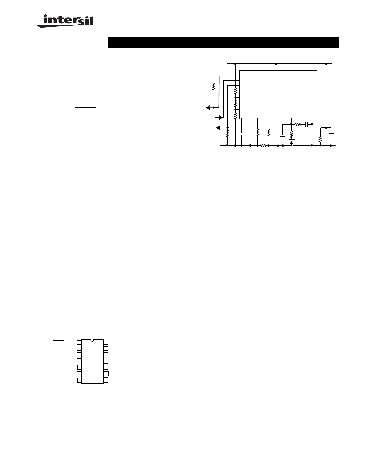
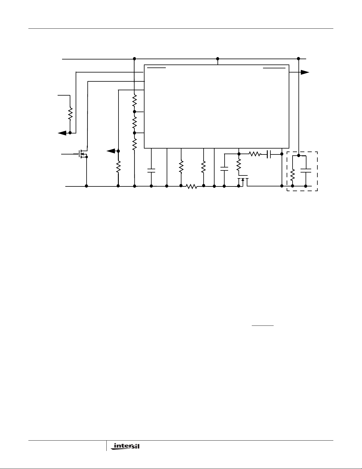
Typical Application
Logic
Supply
R10
R1 = 0.02Ω (1%)
R2 = 10
R3 = 18K
R4 = 549K
R5 = 6.49KΩ
GND GND
V
DD
ISL6142/ISL6152
IS+
SENSE
R7
R8
R1
Ω
(1%)
Ω
(1%)
Ω
(10%)
-48V IN
Ω
(5%)
Ω
(5%)
Ω
R4
R5
R6
R9
(1%)
(1%)
FAULT
DIS
IS
OUT
UV
OV
V
CT
IS-
EE
C3
R6 = 10KΩ (1%)
R7 = R8 = 400
R9 = 4.99K
R10 = 5.1K
C1 = 150nF (25V)
PWRGD
PWRGD
GATE DRAIN
R3
C1
C2
R2
Q1
C2 = 3.3nF (100V)
C3 = 1500pF (25V)
Q1 = IRF530
CL = 100uF (100V)
RL = Equivalent load
LOAD
CL
RL
-48V OUT
Features
• Operates from -20V to -80V (-100V Absolute Max Rating)
• Programmable Inrush Current
• Programmable Time-Out
• Programmable Current Limit
• Programmable Ov er-Voltage Protection
• Programmable Under-Voltage Protection
- 135 mV of hysteresis ~4.7V of hysteresis at the power supply
•V
Under-Voltage Lock-Out (UVLO) ~ 16.5V
DD
TM
• IntelliTrip
severe and moderate faults
- Fast shutdown for short circuit faults with a single retry (fault
current > 4X current limit value).
•FAULT pin reports the occurrence of an Over-Current Time-Out
• Disable input control s GATE shutdo wn a nd resets Ov e r-Current
fault latch
• Load Current Monitor Function
-IS
- A resistor from IS
conversion
• Power Good Control Output
- Output latched “good” when DRAIN and GATE voltage
thresholds are met.
-(PWRGD
- PWRGD active high: ISL6152 (H version)
• Pb-free available
Electronic Circuit Breaker distinguishes between
provides a scaled version of the load current
OUT
to -VIN provides current to voltage
OUT
active low: ISL6142 (L version)
Applications
• Vo IP (Voice over Internet Protocol) Servers
• Telecom systems at -48V
• Negative Power Supply Control
• +24V Wireless Base Station Power
1
CAUTION: These devices are sensitive to electrostatic discharge; follow proper IC Handling Procedures.
1-888-INTERSIL or 321-724-7143
| Intersil and Design is a registered trademark of Intersil Americas Inc.
Copyright © Intersil Americas Inc. 2002, 2004, All Rights Reserved
Intellitrip™ is a trademark of Intersil Americas Inc.

ISL6142, ISL6152
www.BDTIC.com/Intersil
Ordering Information
PKG.
PART NUMBER TEMP. RANGE (oC) PACKAGE
ISL6142CB 0 to 70 14 Lead SOIC M14.15
ISL6142CBZA
(See Note)
ISL6152CB 0 to 70 14 Lead SOIC M14.15
ISL6152CBZA
(See Note)
ISL6142IB -40 to 85 14 Lead SOIC M14.15
ISL6142IBZA
(See Note)
ISL6152IB -40 to 85 14 Lead SOIC M14.15
ISL6152IBZA
(See Note)
*Add “-T” suffix to part number for tape and reel packaging.
NOTE: Intersil Pb-free products employ special Pb-free material
sets; molding compounds/die attach materials and 100% matte tin
plate termination finish, which is compatible with both SnPb and
Pb-free soldering operations. Intersil Pb-free products are MSL
classified at Pb-free peak reflow temperatures that meet or exceed
the Pb-free requirements of IPC/JEDEC J Std-020B.
0 to 70 14 Lead SOIC
(Pb-free)
0 to 70 14 Lead SOIC
(Pb-free)
-40 to 85 14 Lead SOIC
(Pb-free)
-40 to 85 14 Lead SOIC
(Pb-free)
DWG. #
M14.15
M14.15
M14.15
M14.15
2
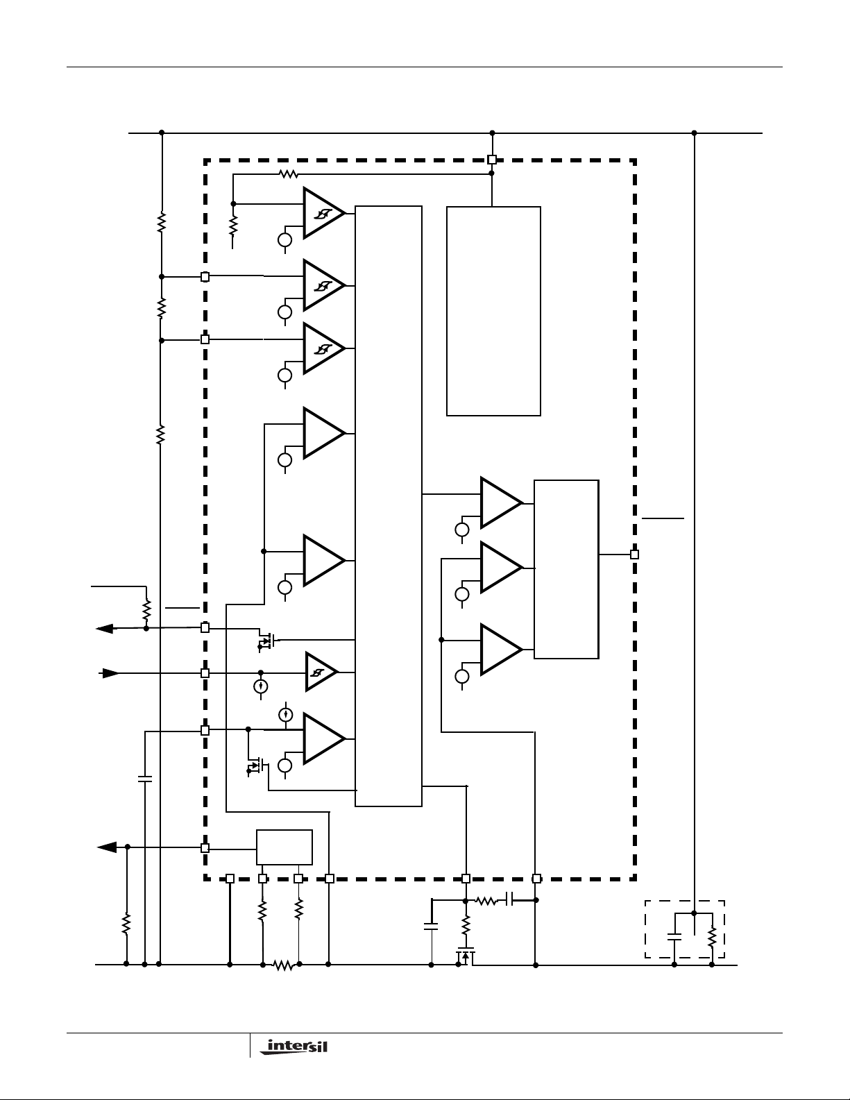
ISL6142, ISL6152 Block Diagram
www.BDTIC.com/Intersil
ISL6142, ISL6152
LOGIC
SUPPLY
LOGIC
INPUT
R10
C3
R4
R5
R6
GND
FAULT
UV
OV
DIS
CT
GND
V
DD
-
1.265V
+
+
V
EE
-
V
1.255V
+
V
1.255V
+
V
EE
-
+
EE
+
-
EE
UVLO
REGULATOR,
REFERENCES
UV
13V
OV
LOGIC,
TIMING,
GATE
DRIVE
-
210mV
+
+
V
EE
-
50mV
+
+
V
EE
V
EE
13V
V
EE+5V
-
8.5V
+
+
-
V
V
EE
EE
HARD
FAULT
GATE
CURRENT
LIMIT
REGULATOR
FAULT
DISABLE
TIMER
GATE
STOP
11. 1V
+
V
1.3V
+
V
8.0V
+
V
-
+
PWRGD
EE
-
+
EE
-
+
EE
LATCH,
LOGIC,
OUTPUT
DRIVE
(ISL6142)
PWRGD
(ISL6152)
CURRENT
TO ADC
-48V IN
R9
IS
OUT
SENSE
V
IS-
EE
R7
R8
IS+
SENSE
C1
R1
GATE DRAIN
C2
R3
R2
Q1
FIGURE 1. BLOCK DIAGRAM
3
LOAD
CL
RL
-48V OUT

ISL6142, ISL6152
www.BDTIC.com/Intersil
Pin Descriptions
PWRGD (ISL6142; L Version) Pin 1 - This digital output is
an open-drain pull-down de vice and can be used to directly
enable an external module. During start-up the DRAIN and
GATE voltages are monitored with two separate comparators.
The first comparator looks at the DRAIN pin v oltage compared
to the internal V
voltage drop across the exte rnal FET and sense resistor.
When the DRAIN to V
first of two conditions required for the po we r to be considered
good are met. In addition, the GATE voltage monitored b y th e
second comparator must be within approxima tely 2.5V of its
normal operating voltage (13.6V). When both criteria are met
the PWRGD
active state, enabling the external module. When this occurs
the two comparators discussed above no longer control the
output. However a third comparator continues to monitor the
DRAIN voltage, and will driv e the PWR GD
the DRAIN voltage raises more than 8V abo ve V
addition, any of the signals that shut off the GATE (OverV oltag e , Unde r-Voltage, Under-Voltage Lock-Out, OverCurrent time-out, pulling the DIS pin high, or powering down)
will reset the latch and drive the PWRGD
disable the module. In this case, the output pull-down device
shuts off, and the pin becomes high impedance. Typically an
external pull-up of some kind is u sed to pull the pin high (man y
brick regulators have a pul l-up functi on built in).
PWRGD (ISL6152; H Version) Pin 1 - This digital output is
used to provide an active high signal to enable an external
module. The Power Good comparators are the same as
described above, but the active state of the output is
reversed (reference figure 37).
When power is considered good (both DRAIN and GATE are
normal) the output is latched in the active high state, the
DMOS device (Q3) turns on and sinks current to V
a 6.2KΩ resistor. The base of Q2 is clamped to V
off. If the external pull-up current is high enough (>1mA, for
example), the voltage drop across th e resistor will be large
enough to produce a logic high output and enable the e xternal
module (in this example, 1mA x 6.2KΩ = 6.2V).
Note that for all H versions, although this is a digital pin
functionally , the logic high lev el is determined by the external
pull-up device, and the power supply to which it is
connected; the IC will not clamp it below the V
Therefore, if the external device does not have its own
clamp, or if it would be damaged by a high voltage, an
external clamp might be necessary.
If the power good latch is reset (GA TE turns off), the internal
DMOS device (Q3) is turned off, and Q2 (NPN) turns on to
clamp the output one diode drop above the DRAIN voltage to
produce a logic low, indicating power is no longer good.
reference (1.3V); this measures the
PG
voltage drop is less than 1.3V, the
EE
output will transition low and be latched in the
output inactive if
. In
EE
output high to
through
EE
to turn it
EE
voltage.
DD
FAULT
Pin 2- This digital output is an open-drain, pull-down
device, referenced to V
the Over-Current latch is set. It goes to a high impedance
state when the fault latch is reset by toggling the UV or DIS
pins. An external pull-up resistor to a logic supply (5V or
less) is required; the fault outputs of multiple IC’s can be
wire-OR’d together. If the pin is not used it should be left
open.
DIS Pin 3 - This digital input disables the FET when driven to
a logic high state. It has a weak internal pull-up device to an
internal 5V rail (10µA), so an open pin will also act as a logic
high. The input has a nominal trip point of 1.6 V while rising,
and a hysteresis of 1.0V. The threshold voltage is referenced
to V
, and is compatible with CMOS logic levels. A logic
EE
low will allow the GATE to turn on (assuming the 4 other
conditions described in the GA TE section are also true). The
DIS pin can also be used to reset the Over-Current latch
when toggled high to low. If not used the pin should be tied to
the negative supply rail (-V
OV (Over-Voltage) Pin 4 - This analog input compares the
voltage on the pin to an internal voltage reference of 1.255 V
(nominal). When the input goes above the reference the
GATE pin is immediately pulled low to shut off the external
FET . The built in 25mV hysteresis will k eep the GATE off until
the OV pin drops below 1.230V (the nominal high to low
threshold). A typical application will use an external resistor
divider from V
resistor divider can be used to set both OV and UV trip
points to reduce component count.
UV (Under-Voltage) Pin 5 - This analog input compares the
voltage on the pin to an internal comparator with a built in
hysteresis of 135mv. When the UV input goes be low the
nominal reference voltage of 1.120V, the GATE pin is
immediately pulled low to shut off the external FET. The
GATE will remain off until the UV pin rises above a 1.255V
low to high threshold. A typical application will use an
external resistor divider from V
as desired. A three-resistor divider can be used to set both
OV and UV trip points to reduce component count.
The UV pin is also used to reset the Over-Current latch. The
pin must be cycled below 1.120V (nominal) and then above
1.255V (nominal) to clear the latch and initiate a normal
start-up sequence.
IS- Pin 6 - This analog pin is the negative input of the current
sense circuit. A sensing resistor (R7) is connected between
this pin and the V
defines the I
sensing is not used in the application, the IS- pin should be
tied directly to the IS+ pin and the node should be left
floating.
to -VIN to set the OV trip level. A three-
DD
EE
SENSE
. It is pulled active low whenever
EE
).
IN
to -VIN to set the UV level
DD
side of resistor R1. The ratio of R1/R7
to IS
current scaling factor . If current
OUT
4

ISL6142, ISL6152
www.BDTIC.com/Intersil
VEE Pin 7 - This is the most Negative Supply Voltage, such
as in a -48V system. Most of the other signals are referenced
relative to this pin, e ven though it may be far aw a y from wh at
is considered a GND reference.
SENSE Pin 8 - This analog input monitors the voltage drop
across the external sense resistor to determine if the current
flowing through it exceeds the programmed Over-Current trip
point (50mV / Rsense). If the Over-Current threshold is
exceeded, the circuit will regulate the current to maintain a
nominal voltage drop of 50mV across the R1 sense resistor,
also referred to as Rsense. If current is limited for more than
the programmed time-out period the IntelliTrip
circuit breaker will trip and turn off the FET.
A second comparator is employed to detect and respond
quickly to hard faults. The threshold of this comparator is set
approximately four times higher (210mV) than the OverCurrent trip point. When the hard fault comparator threshold
is exceeded the GATE is immediately (10µs typical) shut off
(V
= VEE), the timer is reset, and a single retry (soft
GATE
start) is initiated.
IS+ Pin 9 - This analog pin is the positive input of the current
sense circuit. A sensing resistor (R8) is connected between
this pin and the output side of R1, which is also connected to
the SENSE pin. It should match the IS- resistor (R7) as
closely as possible (1%) to minimize output current error
(IS
). If current sensing is not used in the application, the
OUT
IS+ pin should be tied directly to the IS- pin and the node
should be left floating.
GATE Pin 10 - This analog output drives the gate of the
external FET used as a pass transistor. The GATE pin is high
(FET is on) when the following conditions are met:
•V
UVLO is above its trip point (~16.5V)
DD
• V oltage on the UV pin is above its trip point (1.255V)
• V oltage on the OV pin is below its trip point (1.255V)
• No Over-Current conditions are present.
• The Disable pin is low.
If any of the 5 conditions are violated, the GATE pin will be
pulled low to shut off or regulate current through the FET.
The GATE is latched off only when an Over-Current event
exceeds the programmed time-out period.
TM
electronic
1.3v and 8.0V. At initial start-up the DRAIN to V
differential must be less than 1.3V, and the GATE voltage
must be within 2.5V of its normal operating voltage (13.6V)
for power to be considered good. When both conditions are
met, the PWRGD
state. At this point only the 8V DRAIN comparator can
control the PWRGD
if the DRAIN voltage exceeds V
IS
Pin 12 - This analog pin is the output of the current
OUT
sense circuit. The current flowing out of this pin (IS
proportional to the current flowing through the R1 sense
resistor (I
defined by the resistor ratio of R1/R7. Current to voltage
conversion is accomplished by placing a resistor from this
pin to -V
the internal 13V regulator and should not exceed 600µA.
The output voltage will clamp at approximately 8V. If current
sensing is not used in the application the pin should be left
open.
CT Pin 13 - This analog I/O pin is used to program the OverCurrent Time-Out period with a capacitor connected to the
negative supply rail (-V
normal operation, the pin is pulled down to V
current limiting, the capacitor is charged with a 20µA
(nominal) current source. When the CT pin charges to 8.5V,
it times out and the GATE is latched off. If the short circuit
goes away prior to the time-out, the GATE will remain on. If
no capacitor is connected, the time-out will be much quicker,
with only the package pin capacitance (~ 5 to 10 pF) to
charge. If no external capacitor is connected to the CT pin
the time-out will occur in a few µsec. To set the desired timeout period use:
dt = (C * dV) / I = (C * 8.5) / 20 µA = 0.425*10
NOTE: The printed circuit board’s parasitic capacitance (CT pin to
the negative input, -V
calculating the value of C3 needed for the desired time-out.
VDD Pin 14 - This is the most positive Power Supply pin. It
can range from the Under-Volta ge lockout threshold (16.5V)
to +80V (Relative to V
without damage to the IC.
SENSE
IN
/PWRGD output is latched into the active
/PWRGD output, and will drive it inactive
by more than 8.0V.
EE
). The scaling factor, IS
. The current flowing out of the pin is supplied by
which is equal to VEE). During
IN
) should be taken into consideration when
IN
). The pin can tolerate up to 100V
EE
OUT/ISENSE
EE
. During
EE
6
* C
voltage
) is
OUT
is
The GATE is driven high by a weak (-50µA nominal) pull-up
current source, in order to slowly turn on the FET. It is driven
low by a 70mA (nominal) pull-down device for three of the
above shut-off conditions. A larger (350mA nominal) pulldown current shuts off the FET very quickly in the event of a
hard fault where the sense pin voltage exceeds
approximately 210mV.
DRAIN Pin 11 - This analog input monitors the voltage of
the FET drain for the P ower Good function. The DRAIN input
is tied to two comparators with internal reference voltages of
5

ISL6142, ISL6152
www.BDTIC.com/Intersil
.
Absolute Maximum Ratings Thermal Information
Supply Voltage (VDD to VEE). . . . . . . . . . . . . . . . . . . .-0.3V to 100V
DRAIN, PWRGD
UV, OV Input Voltage. . . . . . . . . . . . . . . . . . . . . . . . . . .-0.3V to 60V
SENSE, GATE Voltage . . . . . . . . . . . . . . . . . . . . . . . . . -0.3V to 20V
, DIS, IS+, IS-, IS
FAULT
ESD Rating
Human Body Model (Per MIL-STD-883 Method 3015.7). . .2000V
, PWRGD Voltage. . . . . . . . . . . . . . .-0.3V to 100V
, CT . . . . . . . . . . . . . . . . . -0.3V to 8.0V
OUT
Thermal Resistance (Typical, Note 1) θ
14 Lead SOIC . . . . . . . . . . . . . . . . . . . . . . . . . . . . . 70
Maximum Junction Temperature (Plastic Package) . . . . . . . .150
Maximum Storage Temperature Range. . . . . . . . . . -65
Maximum Lead Temperature (Soldering 10s) . . . . . . . . . . . . .300
Operating Conditions
Temperature Range (Industrial) . . . . . . . . . . . . . . . . . -40oC to 85oC
Temperature Range (Commercial). . . . . . . . . . . . . . . . . 0
Supply Voltage Range (Typical). . . . . . . . . . . . . . . . . . . 36V to 72V
CAUTION: Stresses above those listed in “Absolute Maximum Ratings” may cause permanent damage to the device. This is a stress only rating and operation of the
device at these or any other conditions above those indicated in the operational sections of this specification is not implied.
NOTES:
is measured with the component mounted on a high effective thermal conductivity test board in free air. See Tech Brief TB379 for details.
1. θ
JA
2. PWRGD is referenced to DRAIN; V
PWRGD-VDRAIN
o
C to 70oC
= 0V.
(oC/W)
JA
o
C to 150oC
o
o
C
C
Electrical Specifications V
PARAMETER SYMBOL
DC PARAMETRIC
V
PIN
DD
Supply Operating Range V
Supply Current I
UVLO High V
UVLO Low V
UVLO hysteresis 1.9 V
GATE PIN
GATE Pin Pull-Up Current I
GATE Pin Pull-Down Current I
GATE Pin Pull-Down Current I
GATE Pin Pull-Down Current I
External Gate Drive (at 20V, at 80V) ∆V
GATE High Threshold (PWRGD
SENSE PIN
Current Limit Trip Voltage V
Hard Fault Trip Voltage HFTV HFTV = (V
SENSE Pin Current I
UV PIN
UV Pin High Threshold Voltage V
UV Pin Low Threshold Voltage V
UV Pin Hysteresis V
= +48V, VEE = +0V Unless Otherwise Specified. All tests are over the full temperature range; either
DD
Commercial (0
/PWRGD active) V
o
C to 70oC) or Industrial (-40oC to 85oC). Typical specs are at 25oC.
TEST CONDITIONS MIN TYP MAX UNITS
DD
UV = 3V; OV = VEE; SENSE = VEE; VDD =
DD
80V
UVLOHVDD
UVLOLVDD
PU
PD1
PD2
PD3
GATE(VGATE - VEE)
GH
CL
SENSEVSENSE
UVH
UVL
UVHY
Low to High transition 15 16.7 19 V
High to Low transition 13 15.0 17 V
GATE Drive on, V
GATE Drive off, UV or OV false 70 mA
GATE Drive off, Over-Current Time-Out 70 mA
GATE Drive off; Hard Fault, Vsense > 210mv 350 mA
∆V
VCL = (V
UV Low to High Transition 1.240 1.255 1.270 V
UV High to Low Transition 1.105 1.120 1.145 V
- V
GATE
= 50mV - 0 -0.5 µA
GATE = VEE
, 20V <=VDD <=80V 12 13.6 15 V
GATE
- VEE) 405060mV
SENSE
- VEE) 210 mV
SENSE
20 - 80 V
-30 -50 -60 µA
2.6 4.0 mA
2.5 V
135 mV
6

ISL6142, ISL6152
www.BDTIC.com/Intersil
Electrical Specifications V
= +48V, VEE = +0V Unless Otherwise Specified. All tests are over the full temperature range; either
DD
Commercial (0
o
C to 70oC) or Industrial (-40oC to 85oC). Typical specs are at 25oC. (Continued)
PARAMETER SYMBOL
UV Pin Input Current I
OV pin
OV Pin High Threshold Voltage V
OV Pin Low Threshold Voltage V
OV Pin Hysteresis V
OV Pin Input Current I
DRAIN Pin
Power Good Threshold (Enable PWRGD
/PWRGD
Output)
Drain Input Bias Current I
DRAIN Pin Comparator Trip Point
(PWRGD
ISL6142 (PWRGD
PWRGD
/PWRGD Inactive)
Pin: L Version)
Output Low Voltage V
Output Leakage I
ISL6152 (PWRGD Pin: H Version)
INUVVUV
OVH
OVL
OVHY
INOVVOV
V
PG
DRAINVDRAIN
VDH
OL1
V
OL5
OH
= V
OV Low to High Transition 1.235 1.255 1.275 V
OV High to Low Transition 1.215 1.230 1.255 V
= V
V
DRAIN
V
DRAIN
(V
DRAIN
(V
DRAIN
V
DRAIN
TEST CONDITIONS MIN TYP MAX UNITS
EE
- -0.05 -0.5 µA
25 mV
EE
- V
EE
- -0.05 -0.5 µA
0.80 1.30 2.00 V
= 48V 10 38 60 µA
- V
> 8.0V 7.0 8.0V 9.0 V
EE
- V
< V
EE)
- V
< V
EE)
= 48V, V
PG; IOUT
PG; IOUT
PWRGD
= 1mA - 0.3 0.8 V
= 5mA - 1.50 3.0 V
= 80V - 0.05 10 µA
PWRGD Output Low Voltage (PWRGD-DRAIN) V
PWRGD Output Impedance R
OL
OUT
V
DRAIN
(V
DRAIN
= 5V, I
- V
EE)
= 1mA - 0.80 1.0 V
OUT
< V
PG
4.5 6.2 7.5 kΩ
DIS PIN
DIS Pin High Threshold Voltage V
DIS Pin Low Threshold Voltage V
DIS Pin Hysteresis V
DIS Pin Input High Leakage I
DIS Pin Input Low Current I
PIN
FAULT
FAULT
Output Voltage VF
Output Leakage IF
FAULT
DISH
DISHY
DISINH
DISINL
DIS Low to High Transition 1.60 2.20 3.00 V
DIS High to Low Transition 1.1 1.50 V
DISL
DIS Hysteresis 1.0 V
Input Voltage = 5V 0.1 1.0 µA
Input Voltage = 0V 10 µA
I = 1.6 mA 0.4 V
VOL
V = 5.0V 10 µA
IOH
CT PIN
CT Pin Charging Current I
CT Pin Input Threshold V
IS PINS (IS-, IS+, IS
IS
Error VSENSE = 50mV, R7 = 400Ω, R8 = 404Ω 2.0 %
OUT
Error VSENSE = 200mV, R7 = 400Ω, R8 = 404Ω 1.0 %
IS
OUT
OUT
)
CTINLVCT
CT
= 0V 20 µA
7.5 8.5 9.5 V
ISOUT Offset Current VSENSE = 0.0mV, R7 = 400Ω, R8 = 404Ω 4.5 µA
Output Voltage Range (IS
Pin) 058V
OUT
7

ISL6142, ISL6152
www.BDTIC.com/Intersil
Electrical Specifications V
PARAMETER SYMBOL
AC TIMING
OV High to GATE Low t
OV Low to GATE High t
UV Low to GATE Low t
UV High to GATE High t
DIS Low to GATE Low t
DIS High to GATE High t
GATE Low (Over-Current) to FAULT
IS
Rise Time t
OUT
Fall Time t
IS
OUT
SENSE High to GATE Low t
Current Limit to GATE Low t
Hard Fault to GATE Low (200mV comparator)
Typical GATE shutdown based on application ckt.
Guaranteed by design.
= +48V, VEE = +0V Unless Otherwise Specified. All tests are over the full temperature range; either
DD
Commercial (0
Low t
o
C to 70oC) or Industrial (-40oC to 85oC). Typical specs are at 25oC. (Continued)
TEST CONDITIONS MIN TYP MAX UNITS
PHLOV
PLHOV
PHLUV
PLHUV
PHLDIS
PLHDIS
PHLGF
PHLSENSE
PHLCB
t
PHLHF
Figures 2A, 3A 0.6 1.6 3.0 µs
Figures 2A, 3A 1.0 7.8 12.0 µs
Figures 2A, 3B 0.6 1.3 3.0 µs
Figures 2A, 3B 1.0 8.4 12.0 µs
Figure 2A, 7 0.6 µs
Figure 2A, 7 2.5 µs
Figure 2A, 8 0.5 µs
Figure 2A, 12 1.2 µs
R
Figure 2A, 12 4.0 µs
F
Figures 2A, 9 1 3 µs
Figures 2B, 11, Effective Capacitance During
Test = 2550pF
Figures 10, 20, 33 10.0 µs
1200 µs
ISL6142 (L Version)
DRAIN Low to PWRGD
DRAIN High to PWRGD
GATE High to PWRGD
ISL6152 (H Version)
DRAIN Low to (PWRGD-DRAIN) High (Active) t
DRAIN High to (PWRGD
GATE High to (PWRGD-DRAIN) High (Active) t
Low (Active) t
High (Inactive) t
Low (Active) t
-DRAIN) Low (Inactive) t
PHLDL
PLHDH
PHLGH
PLHDL
PHLDH
PLHGH
Figures 2A, 4A 0.1 3.1 5.0 µs
Figure 2A, 6A 0.2 µs
Figures 2A, 5A 1.0 µs
Figures 2A, 4B 0.1 0.2 5.0 µs
Figure 2A, 6B 0.5 µs
Figures 2A, 5B 0.4 µs
8

?
www.BDTIC.com/Intersil
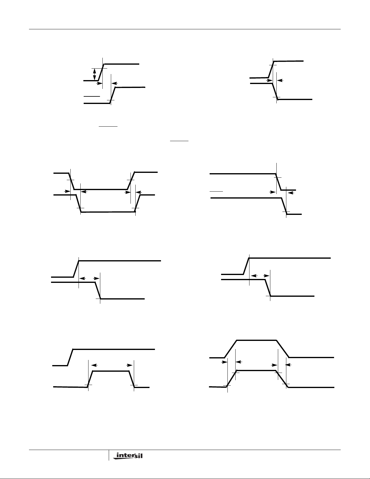
Test Circuit and Timing Diagrams
ISL6142, ISL6152
.
5V
V
DIS
13.6V
0V
2V
0V
GATE
5K
5K
PWRGD
FAULT
V
OV
V
UV
400Ω
V
OV
UV
EE
1
2
3
ISL6142
4
5
6
7
FIGURE 2A. TYPICAL TEST CIRCUIT
1.255V 1.230V
1V
t
PHLOV
t
PLHOV
14
13
12
11
10
9
8
V
DD
4.99K
DRAIN
GATE
404Ω
SENSE
+
-
48V
V
V
SENSE
1V
DRAIN
5V
V
5K
OV
V
5K
UV
PWRGD
FAU LT
OV
UV
V
EE
1
2
3
ISL6142
4
5
6
7
FIGURE 2B. TEST CIRCUIT FOR TIMEOUT
2V
1.125V 1.255V
0V
13.6V
1V
0V
t
PHLUV
UV Pin
GATE
14
13
12
11
10
9
8
V
CT
DRAIN
GATE
SENSE
t
PLHUV
DD
0.1K
9.0K
0.90K
+
48V
-
V
DRAIN
1V
FIGURE 3A. OV TO GATE TIMING
DRAIN
PWRGD
FIGURE 4A. DRAIN TO PWRGD
∆V
- V
GATE
= 0V
GATE
GATE
PWRGD
FIGURE 3B. UV TO GATE TIMING
FIGURE 3. OV AND UV TO GATE TIMING
DRAIN
PG
1.3V
V
EE
t
PHLDL
1.3V
1.0V
V
PG
PWRGD
t
PLHDL
V
1.0V
ACTIVE TIMING (ISL6142) FIGURE 4B. DRAIN TO PWRGD ACTIVE TIMING (ISL6152)
FIGURE 4. DRAIN TO PWRGD
13.6V
V
2.5V
1.0V
t
PHLGH
GH
/PWRGD TIMING
∆V
GATE
GATE
PWRGD
- V
V
PWRGD
GATE
- V
= 0V
DRAIN
1.0V
= 0V
2.5V
t
PLHGH
V
13.6V
GH
FIGURE 5A. GATE TO PWRGD
ACTIVE (ISL6142)
FIGURE 5B. GATE TO PWRGD ACTIVE (ISL6152)
9
ISL6142, ISL6152
www.BDTIC.com/Intersil
Test Circuit and Timing Diagrams (Continued)
- VEE = 8.0V
V
DRAIN
8.0V
1.0V
t
PLHDH
VEE - V
DRAIN
= 0V
V
DH
DRAIN
PWRGD
VEE - V
DRAIN
= 0V
DRAIN
PWRGD
V
- VEE = 8.0V
V
DH
DRAIN
8.0V
1.0V
V
PWRGD
t
PHLDH
- V
DRAIN
= 0V
FIGURE 6A. DRAIN HIGH T O PWRGD ( INA CTI VE) HIGH
(ISL6142)
FIGURE 6. DRAIN TO PWRGD
3V
DIS
GATE
0V
13.6V
0V
1.50V
t
PHLDIS
1V
t
PLHDIS
2.2V
1V
FIGURE 6B. DRAIN HIGH TO PWRGD (INACTIVE) LOW
(ISL6152)
/PWRGD INACTIVE TIMING
∆V
- V
GATE
t
= 0V
1.4V
PHLF
1.0V
GATE
GATE
FAULT
FIGURE 7. DISABLE TO GATE TIMING (ISL6142/52) FIGURE 8. FAULT TO GATE TIMING (ISL6142/52)
0V
13.6V
SENSE
GATE
50mV
t
PHLSENSE
~4V (depends on FET threshold)
0V
13.6V
SENSE
GATE
210mV
t
PHLHF
V
EE
FIGURE 9. SENSE TO GATE (CURRENT LIMIT) TIMING FIGURE 10. SENSE TO GATE (HARD FAULT) TIMING
V
UV
GATE
1.0V
t
PHLCB
1.0V
SENSE
V
OUT
Over-Current Time-Out
FIGURE 11. CURRENT LIMIT TO GATE TIMING FIGURE 12. OUTPUT CURRENT RISE AND FALL TIME
10
10%
t
90%
R
90%
10%
t
F

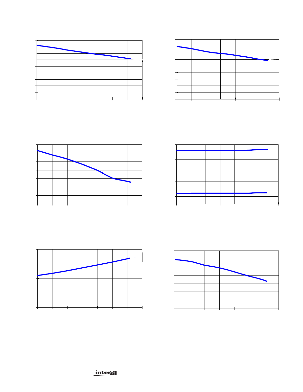
Typical Performance Curves
y
0
www.BDTIC.com/Intersil
ISL6142, ISL6152
4.5
4
3.5
3
2.5
2
IDD (mA)
1.5
1
0.5
0
10 20 30 40 50 60 70 80 90 100
Suppl
FIGURE 13. SUPPLY CURRENT VS. SUPPLY VOLTAGE (25oC) FIGURE 14. GATE VOLTAGE VS SUPPLY VOLTAGE (25oC)
2.75
2.7
2.65
2.6
2.55
2.5
2.45
IDD (mA)
2.4
2.35
2.3
2.25
-40-20 0 20406080100
FIGURE 15. SUPPLY CURRENT VS TEMPERATURE, V
Voltage (VDD)
Temperature (C)
DD
= 80V
16
14
12
10
8
6
4
Gate Voltage (V)
2
0
10 20 30 40 50 60 70 80 100
Supply Voltage (VDD)
14
13.9
13.8
13.7
13.6
13.5
Gate Voltage (V)
13.4
13.3
-40-20 0 20406080100
Temperature (C)
FIGURE 16. GATE VOLTAGE VS TEMPERATURE V
DD
= 48V
50
49
48
47
46
45
44
43
Gate Current (uA)
42
41
-40-20 0 2040608010
Gate Voltage (V)
14
13.9
= 80V
V
13.8
13.7
DD
VDD = 20V
13.6
13.5
13.4
-40-20 0 20406080100
Temperature (C)
FIGURE 17. GATE VOLTAGE VS TEMPERATURE FIGURE 18. GATE PULL-UP CURRENT VS TEMPERATURE
11
Temperature (C)
0
0
ISL6142, ISL6152
www.BDTIC.com/Intersil
90
80
70
60
50
40
30
20
10
0
Gate Pull Down Current (mA)
-40 -20 0 20 40 60 80 10
Temperature (C)
FIGURE 19. GATE PULL-DOWN CURRENT
(UV/OV/TIME-OUT) VS TEMPERATURE
54
52
50
48
46
44
Trip Voltage (mv)
42
40
-40-20 0 204060 80100
450
400
350
300
250
200
150
100
50
0
Gate Pull Down Current (mA)
-40 -20 0 20 40 60 80 10
Temperature (C)
FIGURE 20. HARD FAULT GATE PULL-DOWN CURRENT VS
TEMPERATURE
1.6
5mA
1.4
1.2
1
0.8
0.6
0.4
1mA
0.2
Output Low Voltage (V)
0
-40-20 0 20406080100
Temperature (C)
FIGURE 21. OVER-CURRENT TRIP VOL TAGE VS
TEMPERATURE
2
1.5
1
0.5
Trip Voltage (V)
0
-40-20 0 20 406080100
Temperature (C)
FIGURE 23. DRAIN to PWRGD
VS TEMPERATURE
/ PWRGD TRIP V OL TAGE (VPG)
Temperature (C)
FIGURE 22. PWRGD (ISL6142) VOL VS TEMPERATURE
6.8
6.7
6.6
6.5
6.4
6.3
6.2
Impedance (KOhms)
6.1
-40 -20 0 20 40 60 80 100
FIGURE 24. PWRGD (ISL6152) OUTPUT IMPEDANCE VS
TEMPERATURE
(1 ma)
Temperature (C)
12

ISL6142, ISL6152
www.BDTIC.com/Intersil
6
5
4
3
2
ISOUT Error (uA)
1
0
50 100 150 200
SENSE Pin Voltage (mV)
FIGURE 25. IS
4.475
4.47
4.465
4.46
4.455
4.45
4.445
4.44
ISOUT Offset Current (uA)
4.435
-40-20 0 20406080100
ERROR VS SENSE PIN VOLTAGE FIGURE 26. IS
OUT
VSENSE = 0V
Temperature (C)
-40oC
85oC
2.5
-40oC
2
1.5
1
ISOUT Error (%)
0.5
0
20.5
19.5
18.5
17.5
CT Charging Current (uA)
85oC
050100150
SENSE pin Voltage (mV)
ERROR VS SENSE PIN VOLTAGE
OUT
20
19
18
17
-40-20 0 204060 80100
Temperature (C)
FIGURE 27. ISOUT OFFSET CURRENT VS TEMPERATURE FIGURE 28. CT CHARGING CURRENT VS TEMPERATURE
13
Applications Information
www.BDTIC.com/Intersil
GND GND
ISL6142, ISL6152
FAULT
DIS
Logic
Supply
R4
R10
IS
UV
OUT
R5
OV
R6
V
ADC
Q2
R9
C3
-48V IN
FIGURE 29. TYPICAL APPLICATION WITH MINIMUM COMPONENTS
Typical Values for a representative
system; which assumes:
43V to 71V supply range; 48 nominal; UV = 43V; OV = 71V
EE
V
DD
PWRGD
ISL6142
IS- IS+CT
R7
R8
R1
SENSE GATE DRAIN
C1
R2
R3
C2
Q1
-48V OUT
Quick Guide to Choosing Component
Values
(See fig 29 for reference)
CL
RL
1A of typical current draw; 2.5 Amp Over-Current
100µF of load capacitance (CL); equivalent RL of 48Ω
(R = V/I = 48V/1A)
R1: 0.02Ω (1%)
R2: 10Ω (5%)
R3: 18kΩ (5%)
R4: 549kΩ (1%)
R5: 6.49kΩ (1%)
R6: 10kΩ (1%)
R7/R8: 400Ω (1%)
R9: 4.99KΩ (1%)
R10: 5.10KΩ (10%)
C1: 150nF (25V)
C2: 3.3nF (100V)
C3: 1500pF (25V)
Q1: IRF530 (100V, 17A, 0.11Ω)
Q2: N-Channel logic FET
This section will describe the minimum components needed
for a typical application, and will show how to select
component values. Note that “typical” values may only be
good for this application; the user may have to select
alternate component values to optimize performance for
other applications. Each block will then have more detailed
explanation of how the device works, and alternatives.
R4, R5, R6 - together set the Under-Voltage (UV) and OverVoltag e (OV) trip points. When the power supply ramps up
and down, these trip points (and their hysteresis) will
determine when the GATE is allowed to turn on and off (UV
and OV do not control the PWRGD
input power supply is divided down such that when the
voltage on the OV pin is belo w its threshold and the UV pin is
above its threshold their comparator outputs will be in the
proper state signaling the supply is within its desired
operating range, allowing the GATE to turn on. The
equations below define the comparator thresholds for an
increasing (in magnitude) supply voltage.
R4R5R
V
UV
V
OV
++〈〉
-----------------------------------------
R
R4R5R
++〈〉
-----------------------------------------
6
+()
5R6
6
()
R
6
1.255×=
1.255×=
/ PWRGD output). The
(EQ. 1)
(EQ. 2)
14

ISL6142, ISL6152
www.BDTIC.com/Intersil
The values of R4 = 549K, R5 = 6.49K, and R6 = 10K shown
in figure 29 set the Under-Voltage threshold at 43V, and the
Over-Voltage, turn off threshold to 71V. The Under-Voltage
(UV) comparator has a hysteresis of 135mv’s (4.6V of
hysteresis on the supply) which correlates to a 38.4V turn off
voltage. The Over-Voltage comparator has a 25mv
hysteresis (1.4V of hysteresis on the supply) which
translates to a turn on voltage (supply decreasing) of
approximately 69.6V.
Q1 - is the FET that connects the input supply voltage to the
output load, when properly enabled. It needs to be selected
based on several criteria:
• Maximum voltage expected on the input supply (including
transients) as well as transients on the output side.
• Maximum current and power dissipation expected during
normal operation, usually at a level just below the current
limit threshold.
• Power dissipation and/or safe-operating-area
considerations during current limiting and single retry
events.
• Other considerations include the GATE voltage threshold
which affects the r
(which in turn, affects the
DS(ON)
voltage drop across the FET during normal operation),
and the maximum gate voltage allowed (the IC’s GATE
output is clamped to ~14V).
R1 - is the Over-Current sense resistor also referred to as
R
. If the input current is high enough, such that the
SENSE
voltage drop across R1 exceeds the SENSE comparator trip
point (50mV nominal), the GATE pin will be pulled lower (to
~4V) and current will be regulated to 50mV/Rsense for the
programmed time-out period which is set by C3. The OverCurrent threshold is defined in Equation 3 below. If the timeout period is exceeded the Over-Current latch will be set and
the FET will be turned off to protect the load from excessive
current. A typical value for R1 is 0.02Ω, which sets an OverCurrent trip point of; I
= V/R = 0.05/0.02 = 2.5 Amps. To
OC
select the appropriate value for R1, the user must first
determine at what level of current it should trip, take into
account worst case variations for the trip point (50mV
±10mV = ±20%), and the tolerances of the resistor (typically
1% or 5%). Note that the Over-Current threshold should be
set above the inrush current level plus the expected load
current to avoid activating the current limit and time-out
circuitry during start-up. If the power good output
(PWRGD
/PWRGD) is used to enable an external module,
the desired inrush current only needs to be considered. One
rule of thumb is to set the Over-Current threshold 2-3 times
higher than the normal operating current.
50mv
I
------------------- -=
OC
R
sense
(EQ. 3)
The physical layout of the R1 sense resistor is critical to
avoid the possibility of false ov er current e v ents. Since it is in
the main input-to-output path, the traces should be wide
enough to support both the normal current, and currents up
to the over-current trip point. The trace routing between the
R1 resistor, and the V
and SENSE pins should be direct
EE
and as short as possible with zero current in the sense lines.
Note that in figure 30 the traces from each side of the R1
resistor also connect to the R8 (IS+), and R7 (IS-) current
sensing resistors.
CORRECT
To V
EE
and R7
To SENSE
and R8
FIGURE 30. SENSE RESISTOR LAYOUT GUIDELINES
SENSE RESISTOR
INCORRECT
CURRENT
CL - is the sum of all load capacitances, including the load’s
input capacitance itself. Its value is usually determined by
the needs of the load circuitry, and not the hot plug (although
there can be interaction). For example, if the load is a
regulator, then the capacitance may be chosen based on the
input requirements of that circuit (holding regulation under
current spikes or loading, filtering noise, etc.) The value
chosen will affect the peak inrush current. Note that in the
case of a regulator, there may be capacitors on the output of
that circuit as well; these need to be added into the
capacitance calculation during inrush (unless the regulator is
delayed from operation by the PWRGD
/PWRGD signal).
RL - is the equivalent resistive value of the load and
determines the normal operating current delivered through
the FET. It also affects some dynamic conditions (such as
the discharge time of the load capacitors during a powerdown). A typical value might be 48Ω (I=V/R = 48/48 = 1A).
R2, C1, R3, C2 - are related to the GATE driver, as it
controls the inrush current.
R2 prevents high frequency oscillations; 10Ω is a typical
value. R2 = 10Ω.
R3 and C2 act as a feedback network to control the inrush
current as shown in equation 4, where CL is the load
capacitance (including module input capacitance), and I
PU
is
the GATE pin charging current, nominally 50µA.
I
inrushIPU
-------
×=
C
2
(EQ. 4)
C
L
Begin by choosing a value of acceptable inrush current for
the system, and then solve for C2.
15

ISL6142, ISL6152
www.BDTIC.com/Intersil
C1 and R3 prevent Q1 from turning on momentarily when
power is first applied. Without them, C2 would pull the gate
of Q1 up to a voltage roughly equal to V
*C2/Cgs(Q1)
EE
(where Cgs is the FET gate-source capacitance) before the
ISL6142/52 could power up and actively pull the gate low.
Place C1 in parallel with the gate capacitance of Q1; isolate
them from C2 by R3.
C1 =[(Vinmax - Vth)/Vth] * (C2+Cgd) - where Vth is the
FET’s minimum gate threshold, Vinmax is the maximum
operating input voltage, and Cgd is the FET gate-drain
capacitance.
R3 - its value is not critical, a typical value of 18kΩ is
recommended but values down to 1KΩ can be used. Lower
values of R3 will add delay to gate turn-on for hot insertion
and the single retry event following a hard fault.
R7/R8/R9 - are used to sense the load current (R7/R8) and
convert the scaled output current (IS
) to a voltage (R9)
OUT
that would typically be the input signal to an A to D converter.
R7 is connected between -IS and the R1 sense resistor.
These two resistors set the I
Rsense resistor) to IS
scaling factor based on equation 5
OUT
(current through the
SENSE
below . R8 does not effect the scaling factor but should match
R7 to minimize IS
error. Their tolera nce should be +/-1%,
OUT
which will typically result in an output current error of less than
5% for a full scale co ndition. The tr ace layout is also critical to
obtain optimum performance. The traces connecting these
resistors to the device pins (IS+ and IS-) and to th e R1 sense
resistor should be kept as short as possible, match in length,
and be isolated from the main current flow as illustrated in
figure 30.
response of the current sense circuit for the Over-Current
Time-out and hard fault single retry events.
R10 - is a pull-up resistor for the open drain FAULT
output
pin which goes active low when the Over-Current latch is set
(Over-Current Time-Out). The output signal is referenced to
V
and the resistor is connected to a positive voltage, 5V or
EE
less, with respect to V
. A typical value of 5KΩ is
EE
recommended. A fault indicator LED can be placed in series
with the pull-up resistor if desired. The resistor value should
be selected such that it will allow enough current to drive the
LED adequately (brightness).
C3 - is the capacitor used to program the current limit timeout period. When the Over-Current threshold is exceeded a
20µA (nominal) current source will charge the C3 capacitor
from V
to approximately 8.5V. When the voltage on the CT
EE
pin exceeds the 8.5V threshold, the GATE pin will
immediately be pulled low with a 70ma pull down device, the
Over-Current latch will be set, and the FET will be turned off.
If the Over-Current condition goes away befor e the time-out
period expires, the CT pin will be pulled back down to V
EE
,
and normal operation will resume. Note that any parasitic
capacitance from the CT pin to -V
will effectively add to
IN
C3. This additional capacitance should be taken into account
when calculating the C3 value needed for the desired timeout period.
The value of C3 can be calculated using equation 6 where dt
is the time-out period, dv is the CT pin threshold, and I
CT
is
the capacitor charging current.
C3
dt
------
dv
timeout
×
----------------------
I
CT
8.5V
20
6–
×10×==
(EQ. 6
R9 is used to convert the IS
connected between the IS
current to voltage and is
OUT
pin and -VIN. The current
OUT
flowing through the resistor (EQ. 5) should not e xceed 600µA
and the voltage on the CT pin will clamp at appro xi mately 8V.
R
SENSE
IS
OUTISENSE
-----------------------
×=
R7
(EQ. 5)
To select the appropriate resistor values for the application
the user must first define the R1 sense resistor value and the
maximum load current to be detected/measured. The value
of R7 should then be selected such that the maximum IS
OUT
current is in the 400-500µA range. For example, if the user
wanted to detect and measure fault currents up to the hard
fault comparator trip point (10A); the maximum IS
OUT
current using the application components in figure 23 would
be [10A x (.02/400] = 500µA. The value of R9 should be set
to accommodate the dynamic range of the A to D converter.
For this example, a 5KΩ resistor would produce a full scale
input voltage to the converter of 2.5V (500µA x 5KΩ).
Figures 32 and 33 illustrate the typical output voltage
Q2- is an N-channel logic FET used to drive the disable pin
(DIS). The DIS pin is used to enable/disable the external
pass transistor (Q1) by turning the GATE drive voltage on or
off. The DIS pin can also be used to reset the Over-Current
latch by toggling the pin high and then low. When Q2 is off,
the DIS pin is pulled high with an internal 500KΩ resistor,
connected to an internal +5V (V
+ 5V) supply rail (10µA).
EE
In this condition the GATE pin is low, and Q1 is turned off.
When Q2 is on, the DIS pin is pulled low to V
allowing the
EE
GATE pin to pull up and turn on Q1. The gate of Q2 will
typically be driven low (<1.5V) or High (>3.0V) with external
logic circuitry referenced to the negative input (-V
Low-side Application
IN
).
Although this IC was designed for -48V systems, it can also
be used as a low-side switch for positive 48V systems; the
operation and components are usually similar. One possible
difference is the kind of level shifting that may be nee ded to
interface logic signals to the IC. Fo r e xample , man y of the IC
functions are referenced to the IC substrate, connected to the
V
pin, but this pin may be considered -48V or GND,
EE
depending upon the polarity of the system. Also, the input or
output logic (running at 5V or 3.3V or even lo w er) might be
16
ISL6142, ISL6152
www.BDTIC.com/Intersil
externally referenced to either VDD or VEE of the IC, instead
of GND.
Inrush Current Control
The primary function of the ISL6142/52 hot plug controller is
to control the inrush current. When a board is plugged into a
live backplane , the input cap acito rs of the board’s power
supply circuit can produce large current transients as they
charge up. This can cause glitches on the system po we r
supply (which can affect other boards!), as w ell as possibly
cause some permanent damage to the power supply.
The key to allo wing boards to be inserted into a live bac kplane
is to turn on the power to the board in a controlled manner,
usually by limiting the current allow ed to flow through a FET
switch, until the input capacitors are fully charged. At that
point, the FET is fully on, for the smallest voltage drop across
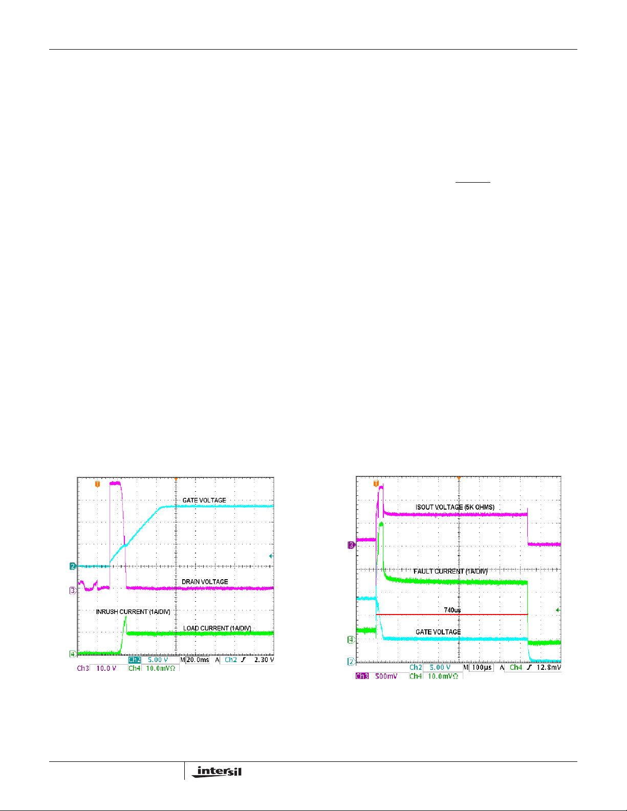
it. Figure 31 illustrates the typical inrush current response for a
hot insertion under the following conditions:
V
= -48V, Rsense = 0.02W
IN
Current limit = 50mV / 0.02Ω = 2.5A
C1 = 150nF, C2 = 3.3nF, R3 = 18kΩ
CL = 100µF, R L = 50Ω, I
I
= 50µA (100µF / 3.3nF) = 1.5A
inrush
After the contact bounce subsides the UVLO and UV criteria
are quickly met and the GATE begins to ramp up. As the
GATE reaches approximately 4V with respect to the source,
the FET begins to turn on allowing current to charge the
100µF load capacitor . As the drain to source v oltage begins to
drop, the feedback network of C2 and R3 hold the GA TE
constant, in this case limiting the current to approximately
1.5A. When the DRAIN voltage completes its r amp do w n, the
load current remains constant at approximately 1.0A as the
GATE voltage increases to its final value.
= 48V / 50Ω ~1.0A
LOAD
excessive supply or fault currents. The IntelliTrip
circuit breaker is capable of detecting both hard faults, and
less severe Ov er-Current co nditions.
The Over-Current trip point is determined by R1 (EQ. 3) also
referred to as Rsense. When the voltage across this resi stor
exceeds 50mV, the current limit regulator will turn on, and the
GATE will be pulled lower (to ~4V) to regulate current through
the FET at 50mV/Rsense. If the fault persists and current
limiting exceeds the progr ammed time-out period, the FET will
be turned off by discharging the GATE pin to V
the Over-Current latch and the PWRGD
transition to the inactive state, indicating p o w er is no longer
good. To clear the latch and initiate a normal start-up
sequence, the user must either pow er down the system
(below the UVLO voltage), toggle the UV pin belo w and abov e
its threshold (usually with an external transistor), or toggle the
DIS pin high to low . Figure 32 shows the Over-Current shut
down and current limiting response for a 10 Ω short to ground
on the output. Prior to the short circuit the output load is 110Ω
producing an operating current of about 0.44A (48V/110Ω). A
10Ω short is then applied to the output causing an initial fault
current of 4.8A. This produces a voltage drop across the
0.02Ω sense resistor of approximately 95mV, roughly two
times the Over-Current threshold of 50mV. The GATE is
quickly pulled low to limit the current to 2.5A (50mV/Rsense)
and the timer is enabled. The f ault conditi on persists for the
duration of the programmed time-out period (C3 = 1500pF)
and the GATE is latched off in about 740µs. There is a short
filter (3µs nominal) on the comparator, so current tr ansients
shorter than this will be ignored. Longer transients will initiate
the GATE pull down, current limiting, and the timer. If the fault
current goes awa y be fore the time-out period expires the
device will ex it the current limiti ng mode and resume normal
operation.
/PWRGD output will
TM
electronic
. This will set
EE
FIGURE 31. HOT INSERTION INRUSH CURRENT LIMITING,
DISABLE PIN TIED TO V
EE
Electronic Circuit Breaker/Current Limit
The ISL6142/52 allows the user to program both the current
limit and the time-out period to protect the system against
17
FIGURE 32. CURRENT LIMITING AND TIME-OUT
In addition to current limiting and programmable time-out,
there is a hard fault comparator to respond to short circuits
with an immediate GATE shutdown (typically 10µs) and a
single retry. The trip point of this comparator is set ~4 times

ISL6142, ISL6152
www.BDTIC.com/Intersil
(210mV) higher than the Over-Current threshold of 50mV. If
the hard fault comparator trip point is exceeded, a hard pull
down current (350mA) is enabled to quickly pull down the
GATE and momentarily turn off the FET. The fast shutdown
resets the timer and is followed by a soft start, single retry
event. If the fault is still present after the GATE is slowly
turned on, the current limit regulator will trip (sense pin
voltage > 50mV), turn on the timer, and limit the current to
50mV/Rsense. If the fault remains and the time-out period is
exceeded the GATE pin will be latched low. Note: Since the
timer starts when the SENSE pin exceeds the 50mV
threshold, then depending on the speed of the current
transient exceeding 200mV; it’s possible that the current limit
time-out and shutdown can occur before the hard fault
comparator trips (and thus no retry). Figure 33 illustrates the
hard fault response with a ze ro ohm short circuit at the output.
within its expected operating range and the GATE will be
allowed to turn on, or remain on. If the UV pin voltage drops
below its high to low threshold, or the OV pin voltage
increases above its low to high threshold, the GATE pin will
be pulled low, turning off the FET until the supply is back
within tolerance.
The OV and UV inputs are high impedance, so the value of
the external resistor divider is not critical with respect to input
current. Therefore, the next consideration is total current; the
resistors will always draw current, equal to the supply
voltage divided by the total resistance of the divider
(R4+R5+R6) so the values should be chosen high enough to
get an acceptable current. However, to the extent that the
noise on the power supply can be transmitted to the pins, the
resistor values might be chosen to be lower . A filter capacitor
from UV to -V
transients need to be filtered. (Note that even some
transients which could momentarily shut off the GATE might
recover fast enough such that the GATE or the output current
does not even see the interruption).
Finally, take into account whether the resistor values are
readily available, or need to be custom ordered. Tolerances
of 1% are recommended for accuracy . Note that f o r a typical
48V system (with a 43V to 72V range), the 43V or 72V is
being divided down to 1.255V , a significant scaling f actor . For
UV, the ratio is roughly 35 times; every 3mV change on the
UV pin represents roughly 0.1V change of power supply
voltage. Conv ersely, an error of 3mV (due to the resistors, for
example) results in an error of 0.1V for the supply trip point.
The OV ratio is around 60. So the accuracy of the resistors
comes into play.
or OV to -VIN is a possibility, if certain
IN
FIGURE 33. HARD FAULT SHUTDOWN AND RETRY
As in the Over-Current Time-Out response discussed
previously, the supply is set at -48V and the current limit is
set at 2.5A. After the initial gate shutdown (10µs) a soft start
is initiated with the short circuit still present. As the GATE
slowly turns on the current ramps up and exceeds the OverCurrent threshold (50mV) enabling the timer and current
limiting (2.5A). The fault remains for the duration of the timeout period and the GATE pin is quickly pulled low and
latched off.
Applications: OV and UV
The UV and OV pins can be used to detect Over-Voltage and
Under-Voltage conditions on the input supply and quickly
shut down the external FET to protect the system. Each pin
is tied to an internal comparator with a nominal reference of
1.255V. A resistor divider between the V
typically used to set the trip points on the UV and OV pins. If
the voltage on the UV pin is above its threshold and the
voltage on the OV pin is below its threshold, the supply is
(gnd) and -VIN is
DD
The hysteresis of the comparators is also multiplied by the
scale factor of 35 for the UV pin (35 * 135mV = 4.7V of
hysteresis at the power supply) and 60 for the OV pin (60 *
25mV = 1.5V of hysteresis at the power supply).
With the three resistors, the UV equation is based on the
simple resistor divider:
1.255 = V
= 1.255 [(R4 + R5 + R6)/(R5 + R6)]
V
UV
Similarly, for OV:
1.255 = V
= 1.255 [(R4 + R5 + R6)/(R6)]
V
OV
Note that there are two equations, but 3 unknowns. Because
of the scale factor , R4 ha s to be m uch bigge r than the other
two; chose its value first, to set the current (f or e xample , 50V /
500kΩ draws 100µA), and then the other two will be in the
10kΩ range. Solv e the tw o equations for two unknowns. Note
that some iteration may be necessary to select values that
meet the requirement, and are also readily av ailab l e standard
values.
The three resistor divider (R4, R5, R6) is the recommended
approach for most applications, but if acceptable v alues can’t
[(R5 + R6)/(R4 + R5 + R6)] or
UV
[(R6)/(R4 + R5 + R6)] or
OV
18

ISL6142, ISL6152
www.BDTIC.com/Intersil
be found, then consider 2 separate resistor dividers (one for
each pin, both from V
to -VIN). This also allows the user to
DD
adjust or trim either trip point independently. Some
applications employ a short pin ground on the connector tied
to R4 to ensure the hot plug device is fully powered up
before the UV and OV pins (tied to the short pin ground) are
biased. This ensures proper control of the GATE is
maintained during power up. This is not a requirement for the
ISL6142/52 however the circuit will perform properly if a
short pin scheme is implemented (reference Figure 38).
Applications: PWRGD/PWRGD
The PWRGD/PWRGD outputs are typically used to directly
enable a power module, such as a DC/DC converter. The
PWRGD
enable (L version), and PWRGD (ISL6152) for those with an
active high enable (H version). The modules usually have a
pull-up device built-in, as well as an internal clamp. If not, an
external pull-up resistor may be needed. If the pin is not
used, it can be left open.
For both versions at initial start-up, when the DRAIN to V
voltage differential is less than 1.3V and the GATE voltage is
within 2.5V (V
power is considered good and the PWRGD
will go active. At this point the output is latched and the
comparators above no longer control the output. However a
second DRAIN comparator remains active and will drive the
PWRGD
exceeds V
the signals that shut off the GATE (Over-Voltage, Und erVoltage; Under-Voltage-Lock-Out; Over-Current Time-Out,
disable pin high, or powering down). In this case the
PWRGD
no longer good.
ISL6142 (L version; Figure 34): Under normal conditions
(DRAIN voltage - V
the Q2 DMOS will turn on, pulling PWRGD
module.
When any of the 5 conditions occur that turn off the GATE
(OV, UV, UVLO, Over-Current Time-Out, disable pin high)
the PWRGD latch is reset and the Q2 DMOS device will shut
off (high impedance). The pin will quickly be pulled high by
the external module (or an optional pull-up resistor or
equivalent) which in turn will disable it. If a pull-up resistor is
used, it can be connected to any supply voltage that doesn’t
exceed the IC pin maximum ratings on the high end, but is
high enough to give acceptable logic levels to whatever
(ISL6142) is used for modules with active low
EE
) of its normal operating voltage (13.6V),
GH
/PWRGD pins
/PWRGD output inactive if the DRAIN voltage
by more than 8V. The latch is reset by any of
EE
/PWRGD output will go inactive, indicating power is
< VPG, and ∆V
EE
GATE
- V
GATE
< VGH)
low, enab ling the
signal it is driving. An external clamp may be used to limit the
voltage range.
∆
V
GATE
V
GH
-
+
GATE
V
PG
+
-
V
EE
V
DH
+
-
V
EE
FIGURE 34. ACTIVE LOW ENABLE MODULE
The PWRGD
VDD
(SECTION OF) ISL6142
(L VERSION)
-
PWRGD
+
+
-
LATCH
Q2
LOGIC
V
EE
+
-
DRAIN
can also drive an opto-coupler (such as a
CL
+
VIN+
VOUT+
ON
/OFF
ACTIVE LOW
ENABLE
MODULE
VIN-
VOUT-
4N25), as shown in Figure 35 or LED (Figure 36). In both
cases, they are on (active) when power is good. Resistors
R13 or R14 are chosen based on the supply voltage, and the
amount of current needed by the loads.
V
DD
(SECTION OF) ISL6142
(L VERSION)
LOGIC
LATCH
COMP ARATORS
FIGURE 35. ACTIVE LOW ENABLE OPTO-ISOLATOR
V
DD
(SECTION OF) ISL6142
(L VERSION)
LOGIC
LATCH
COMP ARATORS
FIGURE 36. ACTIVE LOW ENABLE LED
Q2
Q2
PWRGD
V
EE
V
EE
DRAIN
PWRGD
DRAIN
R13
PWRGD
OPTO
R14
LED (GREEN)
ISL6152 (H version; Figure 37): Under normal conditions
(DRAIN voltage - V
< VPG, and ∆V
EE
GATE
- V
GATE
< VGH),
the Q3 DMOS will be on, shorting the bottom of the internal
resistor to V
, turning Q2 off. If the pull-up current from the
EE
external module is high enough, the voltage drop across the
6.2kΩ resistor will look like a logic high (relativ e to DRAIN).
Note that the module is only ref eren ced to DRAIN, not V
EE
19

ISL6142, ISL6152
www.BDTIC.com/Intersil
(but under normal conditions, the FET is on, and the DRAIN
and V
are almost the same voltage).
EE
When any of the 5 conditions occur that turn off the GA TE, the
Q3 DMOS turns off, and the resistor and Q2 clamp the
PWRGD pin to one diode drop (~0.7V) above the DRAIN pin.
This should be able to pull low against the module pull-up
current, and disable the module.
VDD
∆
V
GATE
GATE
(SECTION OF) ISL6152
V
GH
-
+
(H VERSION)
-
6.2K
+
V
PG
+
+
-
-
V
EE
V
DH
+
+
-
V
EE
FIGURE 37. ACTIVE HIGH ENABLE MODULE
LATCH
LOGIC
-
DRAIN
Q3
Q2
V
EE
PWRGD
CL
+
VIN+
VOUT+
ON/OFF
ACTIVE HIGH
ENABLE
MODULE
VIN-
VOUT-
Applications: GATE Pin
To help protect the external FET, the outp ut of the GATE pin
is internally clamped; up to an 80V supply and will not be any
higher than 15V. Under normal operation when the supply
voltage is above 20V, the GATE voltage will be regulated to a
nominal 13.6V above V
EE
.
a high enough input voltage (remember that current through
the RPG 6.2kΩ resistor generates the high voltage level; see
Figure 34).
The input capacitance of the brick is chosen to match its
system requirements, such as filtering noise, and
maintaining regulation under varying loads. Note that this
input capacitance appears as the load capacitance of the
ISL6142/52.
The brick’s output capacitance is also determined by the
system, including load regulation considerations. Howe v er, it
can affect the ISL6142/52, depending upon how it is
enabled. For example, if the PWRGD
/PWRGD signal is not
used to enable the brick, the following could occur.
Sometime during the inrush current time, as the main power
supply starts charging the brick input capacitors, the brick
itself will start working, and start charging its output
capacitors and load; that current has to be added to the
inrush current. In some cases, the sum could exceed the
Over-Current threshold, which could shut down the system if
the time-out period is exceeded! Therefore, whenever
practical, it is advantageous to use the PWRGD
/PWRGD
output to keep the brick off at least until the input caps are
charged up, and then start-up the brick to charge its output
caps.
Typical brick regulators include models such as Lucent
JW050A1-E or Vicor VI-J30-CY. These are nominal -48V
input, and 5V outputs, with some isolation between the input
and output.
Applications: “Brick” Regulators
One of the typical loads used are DC/DC regulators, some
commonly known as “brick” regulators, (partly due to their
shape, and because it can be considered a “building block”
of a system). For a given input voltage range, there are
usually whole families of different output voltages and
current ranges. There are also various standardized sizes
and pinouts, starting with the original “full” brick, and since
getting smaller (half-bricks and quarter-bricks are now
common).
Other common features may include: all components (except
some filter capacitors) are self-contained in a molded plastic
package; external pins for connections; and often an
ENABLE input pin to turn it on or off. A hot plug IC, such as
the ISL6142 is often used to gate power to a brick, as well as
turn it on.
Many bricks have both logic polarities availab le (Enab le high
or low input); select the ISL6142 (L-version) or ISL6152 (Hversion) to match. There is little difference between them,
although the L-version output is usually simpler to interface.
The Enable input often has a pull-up resistor or current
source, or equivalent built in; care must be taken in the
ISL6152 (H version) output that the given current will create
Applications: Optional Components
In addition to the typical application, and the variations
already mentioned, there are a few other possible
components that might be used in specific cases. See Figure
38 for some possibilities.
If the input power supply exceeds the 100V absolute
maximum rating, even for a short transient, that could cause
permanent damage to the IC, as well as other components
on the board. If this cannot be guaranteed, a voltage
suppressor (such as the SMAT70A, D1) is recommended.
When placed from V
voltage.
If transients on the input power supply occur when the
supply is near either the OV or UV trip points, the GATE
could turn on or off momentarily. One possible solution is to
add a filter cap C4 to the V
R11. A large value of R11 is better for the filtering, but be
aware of the voltage drop across it. For example, a 1kΩ
resistor, with 2.4mA of I
dissipate 2.4mW. Since the UV and OV comparators are
referenced with respect to V
but the GATE clamp voltage could be offset by the voltage
across the extra resistor.
to -VIN on the board, it will clamp the
DD
pin, through isolation resistor
DD
would have 2.4V across it and
DD
they should not be affected,
EE,
20

ISL6142, ISL6152
www.BDTIC.com/Intersil
The switch SW1 is shown as a simple push button. It can be
replaced by an active switch, such as an NPN or NFET; the
principle is the same; pull the UV node below its trip point,
and then release it (toggle low). To connect an NFET, for
example, the DRAIN goes to UV; the source to -V
GATE is the input; if it goes high (relative to -V
, and the
IN
), it turns the
IN
NFET on, and UV is pulled low. Just make sure the NFET
resistance is low compared to the resistor divider, so that it
has no problem pulling down against it.
GND
(SHORT PIN)
GND
Logic
Supply
(VEE+5V)
R10
FAU LT
DIS
IS
OUT
UV
OV
C3
-48V IN
D1*
Logic
Input
R4
R5
C4*
TO
ADC
R6
R9
SW1*
Q2
FIGURE 38. ISL6142/52 OPTIONAL COMPONENTS (SHOWN WITH *)
R12 is a pull-up resistor for PWRGD
, if there is no other
component acting as a pull-up device. The value of R12 is
determined by how much current is needed when the pin is
pulled low (also affected by the V
voltage); and it should
DD
be pulled low enough for a good logic low level. An LED can
also be placed in series with R12, if desired. In that case, the
criteria is the LED brightness versus current.
GND
R11*
V
DD
PWRGD
R12*
ISL6142
V
IS- IS+CT
EE
R7
R1
SENSE GATE DRAIN
C1
R8
Q1
R2
R3
C2
CL
RL
-48V OUT
Applications: Layout Considerations
For the minimum application, there are 10 resistors, 3
capacitors, one IC and 2 FETs. A sample layout is shown in
Figure 39. It assumes the IC is 8-SOIC; Q1 is in a D2P AK (or
similar SMD-220 package).
Although GND planes are common with multi-level PCBs, for
a -48V system, the -48V rails (both input and output) act
more like a GND than the top 0V rail (mainly because the IC
signals are mostly referenced to the lower rail). So if
separate planes for each voltage are not an option, consider
prioritizing the bottom rails first.
Note that with the placement shown, most of the signal lines
are short, and there should be minimal interaction between
them.
Although decoupling capacitors across the IC supply pins
are often recommended in general, this application may not
need one, nor even tolerate one. For one thing, a decoupling
cap would add to (or be swamped out by) any other input
capacitance; it also needs to be charged up when power is
applied. But more importantly, there are no high speed (or
any) input signals to the IC that need to be conditioned. If still
desired, consider the isolation resistor R10, as shown in
figure 38.
NOTE:
1. Layout scale is approximate; routing lines are just for illustration
purposes; they do not necessarily conform to normal PCB
design rules. High current buses are wider, shown with parallel
lines.
2. Approximate size of the above layout is 0.8 x 0.8 inches,
excluding Q1 (D2PAK or similar SMD-220 package).
3. R1 sense resistor is size 2512; all other R’s and C’s shown are
0805; they can all potentially use smaller footprints, if desired.
4. The RL and CL are not shown on the layout.
5. Vias are needed to connect R4 and V
of the board, and R8 to pin 9; all other routing can be on the top
level.
6. PWRGD
signal is not used here.
to GND on the bottom
DD
21

ISL6142, ISL6152
www.BDTIC.com/Intersil
BOM (Bill Of Materials)
R1 = 0.02Ω (5%)
R2 =10.0Ω (5%)
R3 = 18.0KΩ (10%)
R4 = 549KΩ (1%)
R5 = 6.49KΩ (1%)
R6 = 10.0KΩ (1%)
R7 = R8 = 400Ω (1%)
GND
-48V
IN
LOGIC IN
-48V
-48V
+5V
IN
IN
GND
G
S
R10
D
R6
R5
R4
R9 = 4.99KΩ (1%)
R10 = 5.10KΩ (10%)
C1 = 150nF (25V)
C2 = 3.3nF (100V)
C3 = 1500pF (25V)
Q1 = IRF530 (100V, 17A, 0.11)
Q2 = N-channel Logic FEFT
GND
TO
V
DD
R9
C3
1 PG
2 FLT
3 DIS
ISL6142
4 OV
5 UV
6 IS-
7 VEE
R7
VDD 14
CT 13
IS
O 12
D 11
G 10
IS+ 9
S 8
C2
GATE
R3
R2
C1
R8
TO
PIN 9
SOURCE
NFET
DRAIN
-48V OUT
-48V IN
R1
FIGURE 39. ISL6142 SAMPLE LAYOUT (NOT TO SCALE)
22
ISL6142, ISL6152
www.BDTIC.com/Intersil
ISL6142, ISL6152
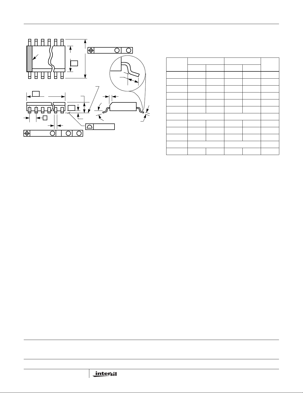
Small Outline Plastic Packages (SOIC)
N
INDEX
AREA
123
-AD
e
B
0.25(0.010) C AM BS
NOTES:
1. Symbols are defined in the “MO Series Symbol List” in Section
2.2 of Publication Number 95.
2. Dimensioning and tolerancing per ANSI Y14.5M-1982.
3. Dimension “D” does not include mold flash, protrusions or gate
burrs. Mold flash, protrusion and gate burrs shall not exceed
0.15mm (0.006 inch) per side.
4. Dimension “E” does not include interlead flash or protrusions.
Interlead flash and protrusions shall not exceed 0.25mm
(0.010 inch) per side.
5. The chamfer on the body is optional. If it is not present, a visual
index feature must be located within the crosshatched area.
6. “L” is the length of terminal for soldering to a substrate.
7. “N” is the number of terminal positions.
8. Terminal numbers are shown for reference only.
9. The lead width “B”, as measured 0.36mm (0.014 inch) or greater above the seating plane, shall not exceed a maximum value
of 0.61mm (0.024 inch).
10. Controlling dimension: MILLIMETER. Converted inch dimensions are not necessarily exact.
E
-B-
SEATING PLANE
A
-C-
M
0.25(0.010) BM M
H
α
µ
A1
0.10(0.004)
L
h x 45
o
M14.15 (JEDEC MS-012-AB ISSUE C)
14 LEAD NARROW BODY SMALL OUTLINE PLASTIC
PACKAGE
INCHES MILLIMETERS
SYMBOL
A 0.0532 0.0688 1.35 1.75 -
A1 0.0040 0.0098 0.10 0.25 -
B 0.013 0.020 0.33 0.51 9
C 0.0075 0.0098 0.19 0.25 D 0.1890 0.1968 4.80 5.00 3
E 0.1497 0.1574 3.80 4.00 4
e 0.050 BSC 1.27 BSC -
C
H 0.2284 0.2440 5.80 6.20 h 0.0099 0.0196 0.25 0.50 5
L 0.016 0.050 0.40 1.27 6
N8 87
o
α
0
o
8
o
0
o
8
Rev. 0 12/93
NOTESMIN MAX MIN MAX
-
All Intersil U.S. products are manufactured, assembled and tested utilizing ISO9000 quality systems.
Intersil Corporation’s quality certifications can be viewed at www.intersil.com/design/quality
Intersil products are sold by description only. Intersil Corporation reserves the right to make changes in circuit design, software and/or specifications at any time without
notice. Accordingly, the reader is cautioned to ver ify that data sheets are current before placing orders. Information furnished by Intersil is believed to be accurate and
reliable. However, no responsibility is assumed by Intersil or its subsidiaries for its use; nor for any infringements of patents or other rights of third par ties which may result
from its use. No license is granted b y implica tion or ot herw ise un der any patent or patent rights of Intersil or its subsidiaries.
For information regarding Intersil Corporation and its products, see www.intersil.com
23
 Loading...