

®
www.BDTIC.com/Intersil
ISL6118
Data Sheet March 2004
Dual Power Supply Controller
The ISL6118 is a dual channel, fully independent overcurrent
(OC) fault protection IC for the +2.5V to +5.5V environment.
This device features internal current monitoring, accurate
current limiting, integrated power switches and current
limited delay to latch-off for system protection.
The ISL6118 current sense and limiting circuitry sets the
current limit to a nominal 0.6A, which is well suited for the
3.3V AUX ACPI application. The ISL6118 is the ideal
companion chip to the HIP1011D and HIP1011E dual PCI
hot plug controllers. Together these and the ISL6118 fully
control the four legacy PCI voltages (±12V, +3.3V, +5V) and
the 3.3V AUX, respectively, for power control of two PCI
slots compliant to PCI Bus Power Management Interface
Spec Rev 1.1. Designed to be co-located with the HIP1011D
on the motherboard, the ISL6118 provides OC fault
notification, accurate current limiting and a consistent timed
latch-off thus isolating and protecting the voltage bus in the
presence of an OC event or short circuit during all PCI Bus
Power States as defined by the PCI specification. The 12ms
time to latch-off is independent of the adjoining switch’s
electrical or thermal condition and the OC response time is
inversely related to the OC magnitude.
Each ISL6118 incorporates in a single 8-lead SOIC
package two 80mΩ N-channel MOSFET power switches
for power control. Each switch is driven by a constant
current source giving a controlled ramp up of the output
voltage. This provides a soft start turn-on eliminating bus
voltage drooping caused by inrush current while charging
heavy load capacitances. Independent enabling inputs and
fault reporting outputs for each channel are compatible with
3V and 5V logic to allow external control and monitoring.
The ISL6118 undervoltage (UV) feature prevents turn-on of
the outputs unless the correct ENABLE state and
VIN > 2.5V are present. During initial turn-on the ISL6118
prevents fault reporting by blanking the fault signal. Rising
and falling outputs are current-limited voltage ramps so that
both the inrush current and voltage slew rate are limited,
independent of load. This reduces supply droop due to
surge and eliminates the need for external EMI filters.
During operation, once an OC condition is detected the
appropriate output is current limited for 12ms to allow
transient conditions to pass. If still in current limit after the
current limit period has elapsed, the output is latched off
and the fault is reported by pulling the corresponding
FAULT
low. The FAULT signal is latched low until reset by
the ENABLE signal being de-asserted at which time the
FAULT
signal will clear.
FN9008.2
Features
• 80mΩ Integrated Power N-Channel MOSFET Switches
• Accurate Current Sensing and Limiting
• 12ms Fault Delay to Latch-Off, No Thermal Dependency
• 2.5V to 5.5V Operating Range
• Disabled Output Internally Pulled Low
• Undervoltage Lockout
• Controlled Turn-On Ramp Time
• Channel Independent Fault Output Signals
• Channel Independent Logic Level Enable High Inputs
(ISL6118H) or Enable Low Inputs (ISL6118L)
• Pb-Free Package Options Available
• Tape & Reel Packing with ‘-T’ Part Number Suffix
Applications
• ACPI 3.3V AUX Control
• Electronic Circuit Limiting and Breaker
Ordering Information
TEMP.
PART #
ISL6118LIB -40 to 85 8 Ld SOIC M8.15
ISL6118LIBZA (Note) -40 to 85 8 Ld SOIC (Pb-free) M8.15
ISL6118HIB -40 to 85 8 Ld SOIC M8.15
ISL6118HIBZA (Note) -40 to 85 8 Ld SOIC (Pb-free) M8.15
ISL6118EVAL1 ISL6118 Evaluation Platform
ISL6AHPEVAL1 ACPI (HIP1011D and ISL6118H) Evaluation
NOTE: Intersil Pb-free products employ special Pb-free material sets;
molding compounds/die attach materials and 100% matte tin plate
termination finish, which is compatible with both SnPb and Pb-free
soldering operations. Intersil Pb-free products are MSL classified at
Pb-free peak reflow temperatures that meet or exceed the Pb-free
requirements of IPC/JEDEC J Std-020B.
RANGE (°C) PKG.
Platform
PKG.
DWG. #
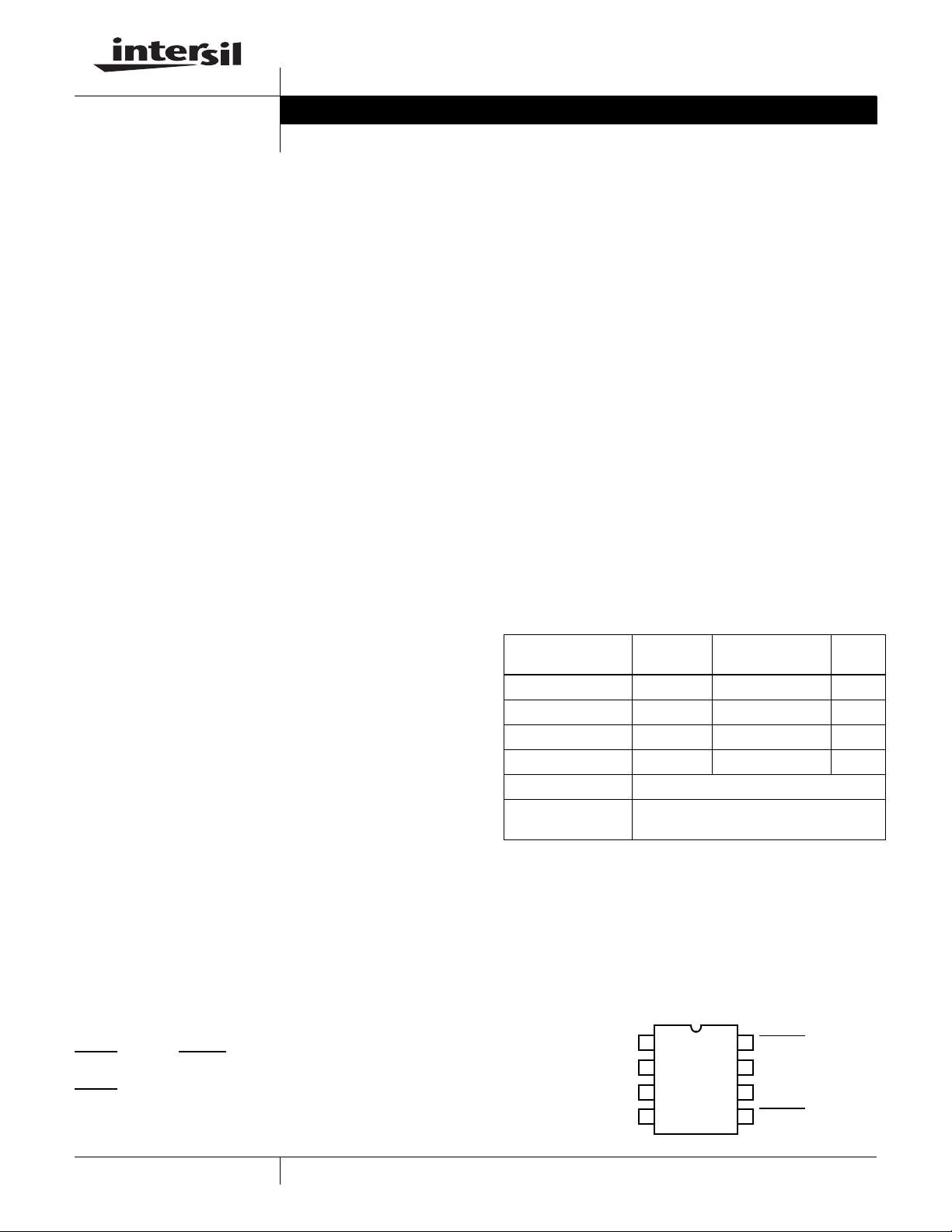
Pinout
ISL6118 (SOIC)
TOP VIEW
GND
VIN
ENABLE_1
ENABLE_2
1
2
3
4
8
7
6
5
FAULT_1
OUT_1
OUT_2
FAULT_2
1
CAUTION: These devices are sensitive to electrostatic discharge; follow proper IC Handling Procedures.
1-888-INTERSIL or 321-724-7143
| Intersil (and design) is a registered trademark of Intersil Americas Inc.
All other trademarks mentioned are the property of their respective owners.
Copyright © Intersil Americas Inc. 2004. All Rights Reserved
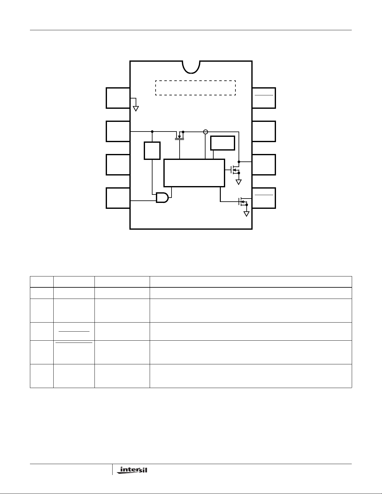
Simplified Block Diagram
www.BDTIC.com/Intersil
GND
ISL6118
CHANNEL 1 LIKE CHANNEL 2
FAULT_1
VIN
Q-PUMP
POR
EN_1
EN_2 FAULT_2
CURRENT AND TEMP.
MONITORING, GATE AND
OUTPUT CONTROL
LOGIC
OUT_1
OUT_2
Pin Descriptions
PIN NO. DESIGNATOR FUNCTION DESCRIPTION
1 GND IC Reference
2 VIN Chip Bias, Controlled
Supply Input,
Undervoltage Lock-Out
VIN provides chip bias voltage. At VIN < 2.5V chip functionality is disabled, FAULT_X latch
is cleared and floating and OUT is held low.
3, 4 ENABLE_1, 2/
ENABLE_1, 2
5, 8 F
6, 7 OUT_2, 1 Channel 2,1 Controlled
AULT OUT_2, 1 Channel 2, 1
Channel Enable/
Enable not Inputs
Overcurrent Fault not
Indicator
Supply Output
Enables/Disables switch.
Channel overcurrent fault-not indicator. FAULT floats and is disabled until VIN > 2.5V. This
output is pulled low after the OC timeout period has expired and stays latched until ENABLE
is deasserted.
Channel voltage output, connect to load to protect. Upon an OC condition OUT is current
limited to 0.6A. Current limit response time is within 200µs. This output will remain in current
limit for a determined time before being latched off.
2
ISL6118
www.BDTIC.com/Intersil
Absolute Maximum Ratings Thermal Information
Supply Voltage (VIN to GND). . . . . . . . . . . . . . . . . . . . . . . . . . . 6.0V
EN, FAULT . . . . . . . . . . . . . . . . . . . . . . . . . . . . . . . . . . . . -0.3V to 6V
OUT . . . . . . . . . . . . . . . . . . . . . . . . . . . . . . .GND-0.3V to VIN +0.3V
Output Current . . . . . . . . . . . . . . . . . . . . . . .Short Circuit Protected
ESD Rating
Human Body Model (Per MIL-STD-883 Method 3015.7) . . . . 3KV
Thermal Resistance (Typical, Note 1)
SOIC Package . . . . . . . . . . . . . . . . . . . . . . . . . . . . . 116
Maximum Junction Temperature . . . . . . . . . . . . . . . . . . . . . . . 150°C
Maximum Storage Temperature Range . . . . . . . . . . . -65°C to 150°C
Maximum Lead Temperature (Soldering 10s) . . . . . . . . . . . . . 300°C
(SOIC - Lead Tips Only)
Operating Conditions
Temperature Range . . . . . . . . . . . . . . . . . . . . . . . . . . .-40°C to 85°C
Supply Voltage Range (Typical) . . . . . . . . . . . . . . . . . . 2.7V to 5.5V
CAUTION: Stresses above those listed in “Absolute Maximum Ratings” may cause permanent damage to the device. This is a stress only rating and operation of the
device at these or any other conditions above those indicated in the operational sections of this specification is not implied.
NOTES:
is measured with the component mounted on a high effective thermal conductivity test board in free air. See Tech Brief TB379 for details.
1. θ
JA
2. All voltages are relative to GND, unless otherwise specified.
θ
JA
(°C/W)
Electrical Specifications Supply Voltages = 3.3V, T
PARAMETER SYMBOL TEST CONDITIONS MIN TYP MAX UNITS
POWER SWITCH
ISL6118 On Resistance at 2.7V r
ISL6118 On Resistance at 3.3V r
ISL6118 On Resistance at 5.0V r
Disabled Output Voltage V
OUT Rising Rate t_vout_rt R
Slow V
Fast V
CURRENT CONTROL
Current Limit, VIN = 3.3V - 5V Ilim V
OC Regulation Settling Time tsett
Severe OC Regulation Settling Time tsett
Overcurrent Latch-off Time t
I/O PARAMETERS
Fault Output Voltage V
ENABLE High Threshold Ven_vih VIN = 5.5V 2.0 - - V
ENABLE Low Threshold at 2.7V Ven_vil VIN = 2.7V - - 0.6 V
ENABLE Low Threshold at 5.5V Ven_vil VIN = 5.5V - - 0.8 V
ENABLE Input Current Ien_i ENABLE = 0V to 5V, VIN = 5V, T
BIAS PARAMETERS
Enabled VIN Current I
Disabled VIN Current I
Undervoltage Lockout Threshold V
UV Hysteresis UV
Over Temperature Disable Temp_dis - 150 - °C
Turn-off Rate t_svout_offt RL = 10Ω, CL = 0.1µF, 90%-10% - 8 - V/ms
OUT
Turn-off Rate t_fvout_offt RL = 1Ω, CL = 0.1µF, 90%-10% - 4 - V/µs
OUT
DS(ON)_27
DS(ON)_33
DS(ON)_50
OUT_DIS
Ilim
Ilim_sevRL
OC_loff
FAULT
VDD
VDD
UVLH
HYS
= T
= -40 to 85°C, Unless Otherwise Specified
A
J
VIN = 2.7V, I
T
= TJ = 85°C - 115 130 mΩ
A
VIN = 3.3V, I
T
= TJ = 85°C - 115 130 mΩ
A
VIN = 5V, I
= TJ = 85°C - 115 130 mΩ
T
A
VIN = 5V, Switch Disabled, 50µA Load - 300 450 mV
= 10Ω, CL = 0.1µF, 10%-90% - 8 - V/ms
L
= 0.8V 0.45 0.6 0.75 A
OUT
RL = 3Ω, CL= 0.1µF to within 10% of CR - 2 - ms
< 1Ω, CL= 0.1µF to within 10% of CR - 100 - µs
ISL6118X, TJ = 25°C - 12 - ms
Fault Output Current = 10mA - - 0.4 V
Switches Closed, OUTPUT = OPEN, TJ > 0°C - 120 200 µA
Switches Open, OUTPUT = OPEN - 1 5 µA
VIN Rising, Switch Enabled 1.7 2.25 2.5 V
= 0.4A, TA = TJ = 25°C - 90 105 mΩ
OUT
= 0.4A, TA = TJ = 25°C - 80 100 mΩ
OUT
= 0.4A, TA = TJ = 25°C - 80 95 mΩ
OUT
> 25°C -0.5 0 0.5 µA
J
50 100 - mV
3

ISL6118
www.BDTIC.com/Intersil
Introduction
The ISL6118 is a fully independent dual channel overcurrent
(OC) fault protection IC for the +2.5V to +5.5V environment.
Each ISL6118 incorporates in a single 8-lead SOIC package
two 80mW N-channel MOSFET power switches for power
control. See Figure 2 for integrated FET on resistance curves.
Independent enabling inputs and fault reporting outputs
compatible with 3V and 5V logic allow for external control and
monitoring. This device features internal current monitoring,
accurate current limiting, integrated power switches and
current limited timed delay to latch-off for system protection.
Key Feature Description and Operation
UV Lockout
The ISL6118 undervoltage (UVLO) lockout prevents
functionality of the device unless the correct ENABLE state
and VIN > 2.5V are present.
Soft Start
A constant 500nA current source ramps up the switch’s gate
causing a voltage follower effect on the output voltage. This
provides a soft start turn-on and eliminates bus voltage
drooping caused by inrush current charging heavy load
capacitances. Rising and falling outputs are current limited
voltage ramps so that both the inrush current and voltage
slew rate are limited, independent of load. This reduces
supply droop due to surge and also eliminates the need for
external EMI filters necessary on other IC products. See
Figure 3 for soft start waveforms.
Fault Blanking on Start-Up
During initial turn-on the ISL6118 prevents nuisance faults
from being reported to the system controller by blanking the
fault signal for 12ms. This blanking eliminates the need for
external RC filters necessary for other vendors’ products.
Current Regulation
The ISL6118 has integrated current sensing on the power
MOSFETs that allows for rapid control of OC events. Once
an OC condition is detected the ISL6118 goes into its current
regulation (CR) control mode. The ISL6118 CR level is set to
a nominal 0.6A and is regulated to within ±25% over full
temperature, bias voltage range and OC magnitude. The
speed of this control is proportional to the level of OC. Thus
a hard OC is more quickly controlled than a marginal
condition. See Figures 4 through 7 for current regulation
performance curves and waveforms.
Latch-Off Time Delay
The primary function of any OC protection device is to
quickly isolate the voltage bus from a faulty load. Unlike
other manufacturers’ IC products that sense the IC thermal
condition to isolate a faulty load, the ISL6118 uses an
internal 12ms timer that starts upon OC detection. Once an
OC condition is detected, the appropriate output is current
limited for 12ms to allow transient conditions to pass before
latch-off. The time to latch-off is independent of the device’s
thermal or adjacent switch’s electrical condition. See Figure
10 for waveforms illustrating independent latch-off.
If, after the ISL6118 has latched off, and the fault has asserted
and the enable is not deasserted but the OC condition still
exists, the ISL6118 (unlike other IC devices) does not send to
the controller a continuous string of fault pulses. The
ISL6118’s single fault signal is sent at the time of latch off.
Slow and Fast Shutdown
The ISL6118 has two shutdown modes. When disabled with
a load current less than the current regulation (CR) level the
ISL6118 shuts down in a controlled manner using a 500nA
constant current source controlled ramp. When disabled
during CR or if the timer has expired the ISL6118 quickly
pulls down the output thereby quickly removing the faulted
load from the voltage bus. See Figures 8 and 9 for illustrative
waveforms of each shutdown mode.
Over Temperature Shutdown
Although the ISL6118 has a thermal shutdown feature,
because of the 12ms timed shutdown this will only be
invoked in extremely high ambient temperatures.
Active Output Pulldown
Another unique ISL6118 feature is the active pull down on the
outputs to 300mV above GND when the device is disabled.
Figure 1 illustrates the ISL6118 operational waveforms,
showing the relationships between the various I/O signals
during typical and faulted conditions. It also graphically
highlights many of the terms and modes of operation
referred to in this data sheet.
Using the ISL6118EVAL1 Platform
General and Biasing Information
The ISL6118EVAL1 platform, Figure 14, allows evaluation of
the ISL6118 dual power supply control IC and comparison
against a suitably sized PPTC component.
The evaluation platform is biased and monitored through
numerous test points (TP#). See Table 1 for test point
assignments and descriptions.
TABLE 1. ISL6118EVAL1 TEST POINT ASSIGNMENTS
TP # DESCRIPTION
TP1 Eval Board and IC GND
TP2 Eval Board +3.3V Bias
TP3 Enable Switch 1
TP4 Enable Switch 2
TP5 Switch 2 Fault
TP6 Switch Out 2
TP7 Switch Out 1
TP8 Switch 1 Fault
TP9 IC VIN Pin
TP10 PPTC Load Side
TP11 Invoke Overcurrent
4

Typical Performance Curves
www.BDTIC.com/Intersil
ENABLE
FAULT
V
OUT
ON
ISL6118
OFF
LATCH-OFF SET
RESET BY
ENABLE
CURRENT REGULATION
SETTLING TIME (1.4ms)
OVERCURRENT
I
OUT
12ms CURRENT REGULATION PERIOD
FIGURE 1. OPERATIONAL WAVEFORMS
120
110
100
90
80
70
60
50
SWITCH ON RESISTANCE (mΩ)
40
-40-30-20-100 102030405060708090
VIN = 2.7V
VIN = 5V
VIN = 3.3V
100
TEMPERATURE (°C)
FIGURE 2. SWITCH ON RESISTANCE AT 0.4A FIGURE 3. V
0.6A CURRENT
LIMIT
ENABLE
CL = 0.1µF
560µs
V
OUT
VOLTAGE (0.5V/DIV)
OUT
OUT
CL = 100µF
CL = 10µF
t
PD
TIME (400µs/DIV)V
SOFT START vs CL and PROP DELAY, Rl = 8Ω
700
-40°C
650
(mA)
600
OUT
I
550
500
1.25 1.5 1.75 2.0 2.25 2.5 2.75 3.0
25°C
85°C
V
OUT
(V)
FIGURE 4. CURRENT REGULATION vs V
(VIN = 3.3V) FIGURE 5. CURRENT REGULATION vs V
OUT
3.1
700
650
(mA)
600
OUT
I
550
500
1.3 1.5 2.0 2.5 3.0 3.5 4.0 4.5
5
-40°C
25°C
85°C
V
OUT
(V)
(VIN = 5V)
OUT
4.8

Typical Performance Curves (Continued)
www.BDTIC.com/Intersil
ISL6118
1.6
1.4
1.2
1.0
0.8
0.6
0.4
0.2
TIME TO CURRENT REGULATION (ms)
0
1 23456789101112
FAULT CURRENT (A)
OUTPUT CURRENT (1A/DIV)
NOMINAL
CURRENT 0.4A
CURRENT REGULATED
LEVEL 0.6A
TIME (200µs/DIV)
FIGURE 6. OC TO CR SETTLING TIME WAVEFORMS FIGURE 7. CR SETTLING TIME vs FAULT CURRENT
ENABLE
CL= 10µF
CL= 100µF
CL= 0.1µF
V
VOLTAGE (0.5V/DIV) TIME (400µs/DIV.)
OUT
FIGURE 8. SLOW TURN-OFF vs C
V
OUT
= 8Ω FIGURE 9. FAST TURN-OFF vs C
L, Rl
V
OUT
CL= 10µF
CL= 100µF
CL= 0.1µF
V
VOLTAGE (0.5V/ DIV) TIME (400µs/DIV)
OUT
LOAD
ISL6118 OUT 1
VOLTAGE (0.5V/DIV)
VIN
ISL6118 OUT 2
TIME (4ms/ DIV)
FIGURE 10. SWITCH FAULT INDEPENDENCE
6

Typical Performance Curves (Continued)
www.BDTIC.com/Intersil
ISL6118
VIN
ISL6118
V
OUT
3.29V (0.075Ω)
V
VIN
3.32V
GND
VOLTAGE (0.5V/DIV)
FIGURE 11. ISL6118 vs PPTC INTO 8.2Ω LOAD FIGURE 12. ISL6118 vs PPTC INTO 3.5Ω LOAD
0.4A HOLD
CURRENT PPTC
2.93V (1.1Ω)
2.3V AT 10s
VOLTAGE (0.5V/DIV) TIME (4ms/DIV)
VIN
0.4A HOLD CURRENT PPTC OUT
1.5V AT 30s
ISL6118 CR
12ms PERIOD
0.4A HOLD CURRENT PPTC OUT
ISL6118 OUT
ISL6118 OUT
VOLTAGE (0.5V / DIV) TIME (4s/DIV)
FIGURE 13. ISL6118 vs PPTC WITH EXTENDED 3.5Ω LOAD
Using the ISL6118EVAL1 Platform
Upon proper bias the PPTC, F1, has a nominal 400mA load
current passing through it which is the hold current rating for
that particular device. Removal of the PPTC is necessary to
isolate the ISL6118 as the PPTC load current is common to
the ISL6118EVAL1 bias connections.
By enabling either or both of the ISL6118H switches by
signaling TP3 and/or TP4 high (>2.4V) these switches are
also loaded with a nominal 400mA current.
Provided test points enable the evaluation of voltage loss
across the PPTC (TP9 - TP10) and likewise across the
ISL6118 enabled switches (TP9 - TP6 and TP7). Expect to
see 100% - 300% greater voltage loss across the PPTC than
the ISL6118 (see Figure 11 for ISL6118 vs PPTC voltage
loss comparison).
An overcurrent (OC) condition can be invoked on both the
ISL6118 and the PPTC by driving TP11 to +6V, causing SW1
to close and a nominal 0.94mA load is imposed. This
represents a current overload to the ISL6118 and is thus
quickly current regulated to the 600mA limit. If the OC
duration extends beyond the nominal 12ms of the internal
ISL6118 timer then the output is latched off and the fault
output is asserted by being pulled low turning on the
appropriate FAULT LED. (Please note: the labeling for the
FAULT-1 and FAULT-2 is reversed.) The eval board is
designed to only invoke a OC condition on channel 2 (TP4)
so that a channel to channel isolation evaluation in the
presence of a OC condition can be evaluated.
The primary function of any OC protection device is to
quickly isolate the voltage bus from a faulty load. Unlike the
PPTC and other vendor available IC products, the ISL6118
internal timer that starts upon OC detection provides
consistent protection that is independent of temperature.
Figures 11 through 13 illustrate the comparative efficiency
and effectiveness of the ISL6118 vs the PPTC in protecting
and isolating a faulty load capable from drooping the system
bus in that system.
7

ISL6118
www.BDTIC.com/Intersil
ISL6118EVAL1
TP2
(VIN)
TP3
TP4
D1
C1
D2
1
VIN OUT1
2
3
EN1
4
EN2
TP9
FAULT_O UT1
ISL6118
FAULT_O UT2
R7
TP10
F1
R6
OUT2
C2
R1
D3
8
TP7
7
TP6
6
5
D4
SW1
R8
C3
R4
R2
R9
C4
R5
R3
D5
R10
FIGURE 14. ISL6118EVAL1 SCHEMATIC AND PHOTOGRAPH
TABLE 2. ISL6118EVAL1 BOARD COMPONENT LISTING
COMPONENT
DESIGNATOR COMPONENT FUNCTION COMPONENT DESCRIPTION
DUT1 ISL6118 Intersil, ISL6118HIB 3.3V Aux Hot Plug Controller
R1 - R3 410mA Nominal Load Resistors YAGEO, 8Ω, 5%, 2W, 8W-2-ND
R4 - R5 970mA Current Over Load Resistors YAGEO, 6Ω, 5%, 2W, 6W-2-ND
R6 - R10 LED Current Limiting Resistor 470Ω, 0805
C1 Decoupling Capacitor 0.1µF, 0805
C2 - C4 Load Capacitor 100µF, 16V Electrolytic, Radial lead
D1 - D5 Indicating LEDs 0805, SMD LEDs Red
F1 PPTC (Polymer Positive Temperature Coefficient) Raychem, Poly Switch, RXE040 or Equivalent
SW1(Q1) Current Over Load Invoking Switch Access TP11 Fairchild, ITF86110DK8T, 7.5A, 30V, 0.025Ω, Dual N-channel, Logic
Level Power MOSFET
8
ISL6118
www.BDTIC.com/Intersil
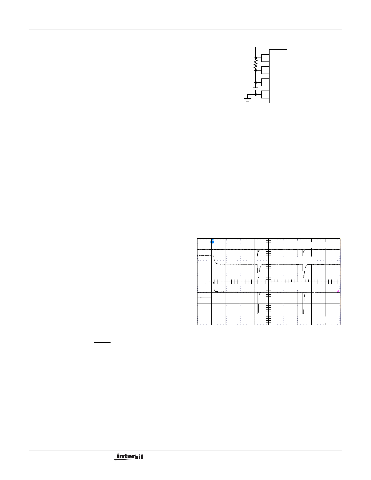
Implementing Autoreset on the ISL6118H
Hot Swap Controllers
Abstract
In applications where the cost, complexity or requirement for
a system controller is avoided and an autonomous power
control function is desired, a device that can monitor and
protect against excessive current failures is needed. This
shows how to implement such an autonomous controller
using the ISL6118HIB. This application works only with the
‘H’ version of these devices. The ‘H’ version refers to the
enable function being asserted upon a high input.
Introduction
The ISL6118, ISL6119 and ISL6121 are all 2.5V to 5V power
supply controllers, each having a different level of current
regulation (CR). The ISL6118 and ISL6119 have 2
independent controllers with CR levels of 0.6A and 1.0A
respectively whereas the ISL6121 is a single supply
controller with a 2A CR level. Each of these devices features
integrated power switch(es) for power control. Each switch
is driven by a constant current source giving a controlled
ramp up of the output voltage. This provides a soft start
turn-on eliminating bus voltage drooping caused by in-rush
current while charging heavy load capacitances. The
independent enabling inputs and fault reporting outputs for
each channel are available and necessary for the
autonomous autoreset application.
The undervoltage (UV) feature prevents turn-on of the
outputs unless the ENABLE pin and VIN are >2.5V. During
initial turn-on the ISL6118 prevents fault reporting by
blanking the fault signal. Rising and falling outputs are
current-limited voltage ramps so that both the inrush current
and voltage slew rate are limited, independent of load. This
reduces supply droop due to surge and eliminates the need
for external EMI filters. During operation, once an OC
condition is detected the appropriate output is current limited
to the appropriate level for 10ms to allow transient conditions
to pass. If still in current limit after the current limit period has
elapsed, the output is latched off and the fault is reported by
pulling the corresponding FAULT
latched low until reset by the ENABLE signal being deasserted at which time the FAULT
It is this described sequence of events that allows for the
autoreset function to be implemented in a cost efficient
manner requiring the addition of only an RC network per
channel to the typical application.
low. The FAULT signal is
signal will clear.
Description of Operation
Rpu = 2K
C = 0.1µF
Initially as voltage is applied to VIN, the pull up resistor (Rpu)
provides for pull up to VIN on both the ENABLE pin asserting
the output once VIN > 2.5V and on the FLTn pin. Once turned
on and an overcurrent (OC) condition occurs the IC provides
CR protection for 10ms and then the FLTn pin pulls low through
Rpu and also pulling the ENABLE low thus resetting the device
fault condition. At this time the Rpu charges the cap and the
voltage on the ENABLE/FLTn node rises until the ENABLE >
2.0 and the output is asserted on once again. This automatic
reset cycle will continue until the OC fault no longer exists on
the output. After several seconds in this mode of operation the
IC thermal protection invokes adjusting the timing of the on-off
cycle to prevent excessive thermal dissipation in the power
switch protecting itself and surrounding circuitry. See Figure 16
for operation waveform.
.
0V
0A
FIGURE 16. AUTO RESET OPERATION
VIN
ISL6118H
FLTn
ENABLE
GND
FIGURE 15.
VIN/FLTn 5V/DIV
VOUT 2V/DIV
IOUT 1A/DIV
4ms/DIV
Applications
•USB
• 2.5V to 5V up to 10W power port protection
Figure 15 illustrates the RC network needed with suggested
component values and the configuration of the relevant pins
for each autoreset channel.
9

Small Outline Plastic Packages (SOIC)
www.BDTIC.com/Intersil
ISL6118
N
INDEX
AREA
123
-AD
e
B
0.25(0.010) C AM BS
NOTES:
1. Symbols are defined in the “MO Series Symbol List” in Section 2.2 of
Publication Number 95.
2. Dimensioning and tolerancing per ANSI Y14.5M-1982.
3. Dimension “D” does not include mold flash, protrusions or gate burrs.
Mold flash, protrusion and gate burrs shall not exceed 0.15mm (0.006
inch) per side.
4. Dimension “E” does not include interlead flash or protrusions. Interlead flash and protrusions shall not exceed 0.25mm (0.010 inch) per
side.
5. The chamfer on the body is optional. If it is not present, a visual index
feature must be located within the crosshatched area.
6. “L” is the length of terminal for soldering to a substrate.
7. “N” is the number of terminal positions.
8. Terminal numbers are shown for reference only.
9. The lead width “B”, as measured 0.36mm (0.014 inch) or greater
above the seating plane, shall not exceed a maximum value of
0.61mm (0.024 inch).
10. Controlling dimension: MILLIMETER. Converted inch dimensions
are not necessarily exact.
E
-B-
SEATING PLANE
A
-C-
M
0.25(0.010) BM M
H
α
µ
A1
0.10(0.004)
L
h x 45
o
C
M8.15 (JEDEC MS-012-AA ISSUE C)
8 LEAD NARROW BODY SMALL OUTLINE PLASTIC
PACKAGE
INCHES MILLIMETERS
SYMBOL
A 0.0532 0.0688 1.35 1.75 -
A1 0.0040 0.0098 0.10 0.25 -
B 0.013 0.020 0.33 0.51 9
C 0.0075 0.0098 0.19 0.25 -
D 0.1890 0.1968 4.80 5.00 3
E 0.1497 0.1574 3.80 4.00 4
e 0.050 BSC 1.27 BSC -
H 0.2284 0.2440 5.80 6.20 -
h 0.0099 0.0196 0.25 0.50 5
L 0.016 0.050 0.40 1.27 6
N8 87
α
0° 8° 0° 8° -
NOTESMIN MAX MIN MAX
Rev. 0 12/93
All Intersil U.S. products are manufactured, assembled and tested utilizing ISO9000 quality systems.
Intersil Corporation’s quality certifications can be viewed at www.intersil.com/design/quality
Intersil products are sold by description only. Intersil Corporation reserves the right to make changes in circuit design, software and/or specifications at any time without
notice. Accordingly, the reader is cautioned to verify that data sheets are current before placing orders. Information furnished by Intersil is believed to be accurate and
reliable. However, no responsibility is assumed by Intersil or its subsidiaries for its use; nor for any infringements of patents or other rights of third parties which may result
from its use. No license is granted by implication or otherwise under any patent or patent rights of Intersil or its subsidiaries.
For information regarding Intersil Corporation and its products, see www.intersil.com
10
 Loading...