

®
www.BDTIC.com/Intersil
ISL6111
Data Sheet March 2004
Current Regulated PCI Hot Plug Power
Switch Controller
The ISL6111 is designed for use in PCI and PCI-X
applications where active current regulation protection of the
motherboard from an abnormal PCI load card is desired.
With the addition of two discrete power MOSFETs and a few
passive components, the ISL6111 provides power control for
the four legacy supplies (-12V, +12V, +5V, +3.3V) to a PCI or
PCI-X slot. This IC integrates the +12V and -12V current
sensing and regulation switches. On the 25W capable 3.3V
and 5V rails, current regulation (CR) protection is provided
by sensing the voltage across external current-sense
resistors and modulation of the gate voltage bias on the
external N-channel power MOSFETs.
During initial power-up of the +12V bias supply, the ENABLE
(EN), Power Good (PG), fault monitoring and reporting
function functions are inhibited if bias voltage <10V. Once
the FETs are enabled they are soft started into the load thus
eliminating supply rail disturbances.
FN9146.1
Features
• Active Current Regulation for Protection
• Adjustable Current Regulation Duration and Magnitude
• Internal MOSFET Switches for +12V and -12V Outputs
• Provides Fault Isolation
• Adjustable Turn-On Slew Rate
• Minimum Parts Count Solution
• No Charge Pump
• 1µs Response Time to Over Current
• Pb-Free leadframe
Applications
•PCI
•PCI-X 1.0
Ordering Information
Upon a failure that quickly causes a load current greater
than the programmed CR level on any voltage supply, the
ISL6111 enters its current regulation (CR) mode, limiting the
load current to the user programmed level for the user
determined period of time. The CR level and duration are set
by a single resistor and capacitor respectively. At the end of
the CR duration all the switches will latch off pulling the
outputs low along with the CRTIM (current regulation timer)
and FLTN (fault not) pins indicating a latch-off due to an over
current (OC) condition. If a severe OC condition should
occur, then the ISL6111 immediately latches off all outputs
and sets the FLTN output low.
During operation, if any of the positive voltages falls below
the minimum PCI specified levels the power good (PG)
output will pull low indicating a non compliant voltage to a
load. PG is an open drain output as is FLTN.
The CRSET pin allows programming of the current
regulation levels to be scaled up or down from the PCI
specified levels via a resistor connected between the
CRSET pin and ground.
All faults and latches are cleared by ENABLE being
deasserted low.
TEMP. RANGE
PART NUMBER
ISL6111CRZA
(see Note)
ISL6111EVAL2 Evaluation Platform
NOTE: Intersil Lead-Free products employ special lead-free
material sets; molding compounds/die attach materials and 100%
matte tin plate termination finish, which is compatible with both SnPb
and lead-free soldering operations. Intersil Lead-Free products are
MSL classified at lead-free peak reflow temperatures that meet or
exceed the lead-free requirements of IPC/JEDEC J Std-020B.
(°C) PACKAGE
0 to 75 20 Ld 5x5 QFN
(Pb-Free)
PKG.
DWG. #
L20.5x5
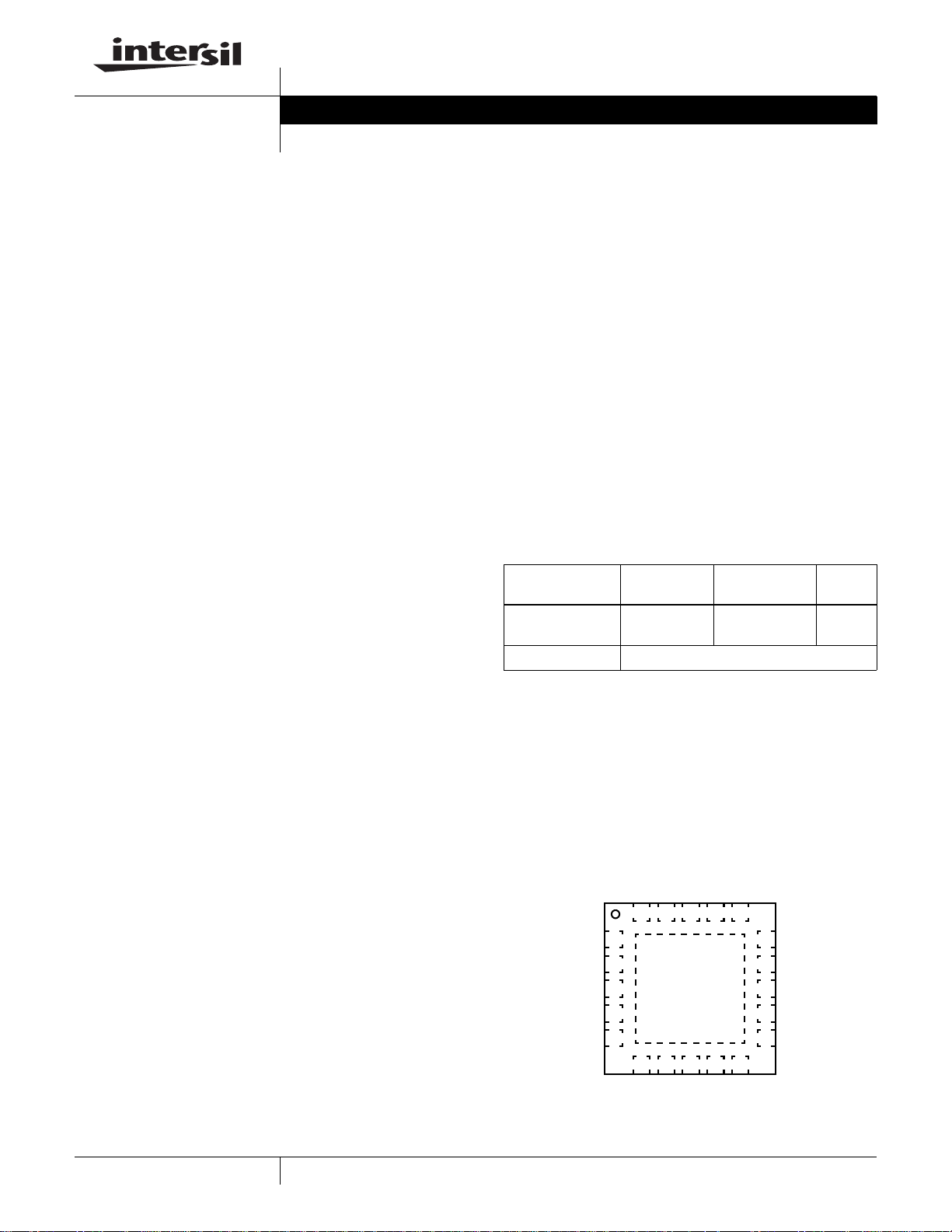
Pinout
ISL6111 (5x5 QFN)
TOP VIEW
3VS
3VISEN
CRSET
M12VO
M12VI
20 19 18 17 16
3VG
12VI_A
GND_B
12VI_B
PGOOD
1
2
3
4
5
-12V
678910
FLTN
CRTIM
5VISEN
5VS
EN
15
14
13
12
11
M12VG
GND_A
12VO_B
12VO_A
5VG
1
CAUTION: These devices are sensitive to electrostatic discharge; follow proper IC Handling Procedures.
1-888-INTERSIL or 321-724-7143
| Intersil (and design) is a registered trademark of Intersil Americas Inc.
All other trademarks mentioned are the property of their respective owners.
Copyright © Intersil Americas Inc. 2004. All Rights Reserved
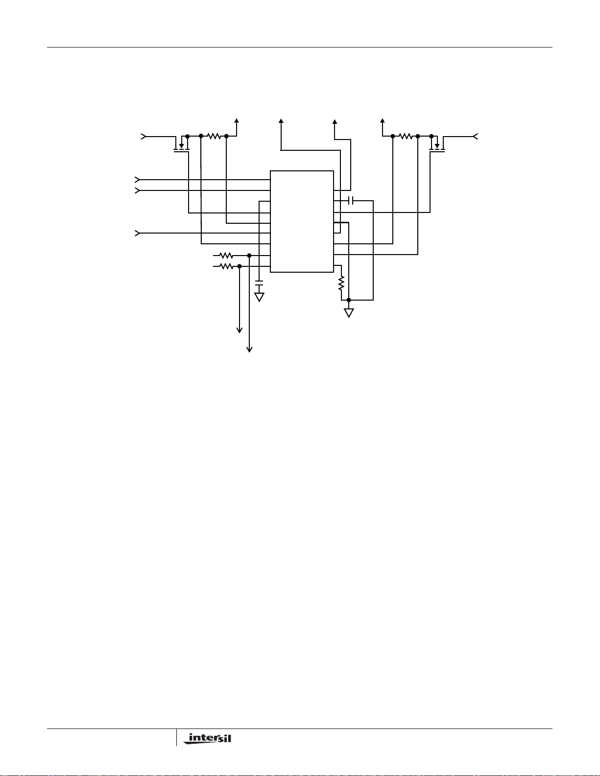
Typical Application
www.BDTIC.com/Intersil
ISL6111
3.3V SUPPLY
ENABLE INPUT
-12V SUPPLY
12V SUPPLY
(Note 1)
V(I/O)
V(I/O)
(Note 1) (Note 1) (Note 1)
3.3V,
7.6A OUT 0.5A OUT 0.1A OUT 5A OUT
R
SENSE_3
FAULTN
12V,
EN
M12VIN
CRTIM
3VG
3VISEN
12VI(2)
3VS
PG
FLTN
C
CRTIM
(Note 2)
POWER GOOD
ISL6111
M12VO
M12VG
GND(2)
12VO(2)
5VISEN
CRSET
R
(Note 1)
-12V,
5VG
5VS
CRSET
5nF
(Note 1)
5V,
R
SENSE_5
(Note 1)
5V SUPPLY
NOTES:
1. See Table 1 for CR level formula
2. See Table 2 for CR duration vs C
.
TIM
FIGURE 1. ISL6111 TYPICAL APPLICATION SCHEMATIC
2
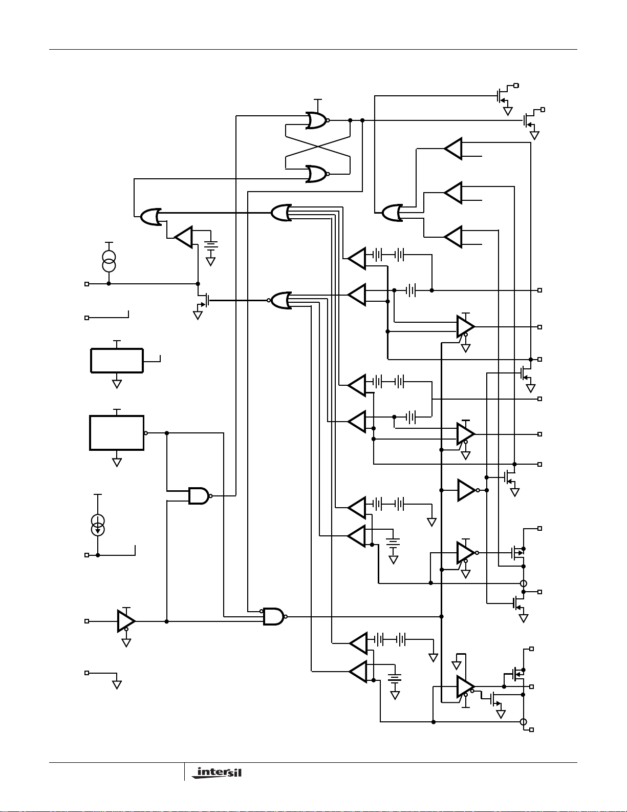
Simplified Schematic
www.BDTIC.com/Intersil
ISL6111
CRTIM
12V
20µA
IN
12V
IN
12V
12V
IN
5V ZENER
REFERENCE
12V
IN
12V
IN
POWER-ON
RESET
COMP
-
+
IN
5V
REF
LOW WHEN 12VIN < 10V
5V
REF
RESET
+
2.8V
-
FAULT
LATCH
COMP
COMP
WOC COMP
-
+
-
+
-
WOC COMP
-
+
-
+
-
COMP
-
4.6V
+
COMP
-
2.9V
+
COMP
-
10.6V
-
+
+
-
+
-
+
+
-
+
+
12V
12V
+
+
-
-
IN
AMP
IN
AMP
PGOOD
FAULTN
5V
S
5V
G
5V
ISEN
3V
S
3V
G
100µA
CRSET
ENABLE
GND
12V
3V
ISEN
IN
V
OCSET
HIGH = FAULT
12V
IN
WOC COMP
-
+
+
-
COMP
HIGH = SWITCHES ON
WOC COMP
COMP
+
+
-
-
+
+
-
-
+
-
+
12V
12VO
M12V
M12VG
M12V
IN
IN
O
12V
IN
AMP
-
+
+
M12V
AMP
IN
-
0.3Ω
0.7Ω
3
ISL6111
www.BDTIC.com/Intersil
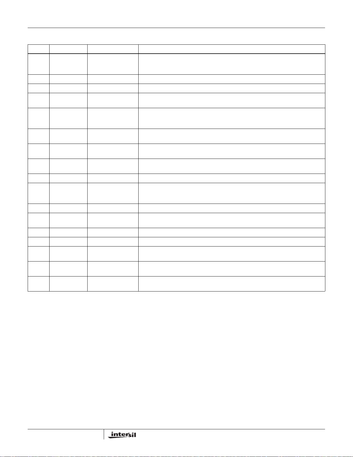
Pin Descriptions
PIN NO. DESIGNATOR FUNCTION FUNCTION DESCRIPTION
1 3VG 3.3V FET Gate Output Drives the gate of the 3.3V MOSFET. Connect to the gate of the external N-Channel
MOSFET. At turn-on the FET gate capacitance will be charged to 12VIN voltage by a 10µA
current source. An optional capacitor from this node to ground will adjust the turn-on ramp.
2, 4 12VI 12V Input +12V IC bias supply and power supply rail input to internal power switch.
3, 14 GND IC Ground Reference Connect to common of power supplies.
5 PGOOD Power Good An open drain logic output that is released to indicate all positive voltage outputs are above
minimum PCI spec. Connect to V(I/O) through resistor.
6 CRTIM Current Regulation
Duration Input
7 FLTN Fault Indication A fault-not open drain output. Latches low once current regulation time has expired. Reset
8 5VISEN 5V Current Sense Connect to the load side of the current sense resistor in series with source of external 5V
9 5VS 5V Source Connect to source of 5V MOSFET switch. This connection along with 5VISEN senses the
10 EN Enable Input Controls all four internal and external switches, initiates turn-on/off
11 5VG 5V FET Gate Output Drives the gate of the 5V MOSFET. Connect to the gate of the external N-Channel
12, 13 12VO Switched 12V Output Switched 12V output.
15 M12VG Gate of Internal NMOS Connect a 5nF capacitor between M12VG and ground to stabilize the start-up ramp for the
16 M12VI -12V Input -12V Supply Input. Also provides power to the -12V current regulation circuitry.
17 M12VO Switched -12V Output Switched -12V Output.
18 CRSET Current Regulation Set Program current regulation levels for all four switches by connecting a resistor to GND. This
19 3VISEN 3.3V Current Sense Connect to the load side of the current sense resistor in series with source of external 3.3V
20 3VS 3.3V Source Connect to source of 3.3V MOSFET. This connection along with 3VISEN senses the voltage
An external capacitor from this pin to ground sets the current regulation duration before
latch off. This output will pull low after the current regulation duration has expired. CR
duration = 150K x CTIM. This pin sources 20µA and has a threshold trip voltage of 2.83V.
by 12VIN POR condition or enable input signaled low. Connect to V(I/O) through resistor.
MOSFET. Monitors voltage to load.
voltage drop across the sense resistor.
MOSFET. At turn-on the FET gate capacitance will be charged to 12VIN voltage by a 10µA
current source. An optional capacitor from this node to ground will adjust the turn-on ramp
M12V supply. This capacitor is charged with 25µA during start-up.
pin sources 100µA. See Table 1 for CR level setting formulae.
MOSFET. Monitors voltage to load.
drop across the sense resistor.
4
ISL6111
www.BDTIC.com/Intersil
Absolute Maximum Ratings Thermal Information
12VI . . . . . . . . . . . . . . . . . . . . . . . . . . . . . . . . . . . . . -0.5V to +15.0V
12VO, 3VG, 5VG . . . . . . . . . . . . . . . . . . . . . . . . -0.5V to 12VI+0.5V
M12VI. . . . . . . . . . . . . . . . . . . . . . . . . . . . . . . . . . . . -14.0V to +0.5V
M12VO, M12VG. . . . . . . . . . . . . . . . . . . . . . . V
3VISEN, 5VISEN . . . . . . . . . . . -0.5V to the Lesser of 12VI or +7.0V
Voltage, Any Other Pin. . . . . . . . . . . . . . . . . . . . . . . . -0.5V to +7.0V
12VO Output Current . . . . . . . . . . . . . . . . . . . . . . . . . . . . . . . . . . .3A
M12VO Output Current . . . . . . . . . . . . . . . . . . . . . . . . . . . . . . . 0.8A
ESD Classification . . . . . . . . . . . . . . . . . . . . . . . . . . . . .4KeV (HBM)
-0.5V to +0.5V
M12VI
Operating Conditions
12VIN Supply Voltage Range . . . . . . . . . . . . . . . . +10.8V to +13.2V
5V and 3.3V Input Supply Tolerances. . . . . . . . . . . . . . . . . . . . . . ±10%
12VO Output Current . . . . . . . . . . . . . . . . . . . . . . . . . . . . .0 to +0.5A
M12VO Output Current . . . . . . . . . . . . . . . . . . . . . . . . . . .0 to +0.1A
Temperature Range (T
CAUTION: Stresses above those listed in “Absolute Maximum Ratings” may cause permanent damage to the device. This is a stress only rating and operation of the
device at these or any other conditions above those indicated in the operational sections of this specification is not implied.
NOTES:
is measured in free air with the component mounted on a high effective thermal conductivity test board with “direct attach” features. See
3. θ
JA
Tech Brief TB379.
4. All voltages are relative to GND, unless otherwise specified.
5. For θ
, the “case temp” location is the center of the exposed metal pad on the package underside.
JC
) . . . . . . . . . . . . . . . . . . . . . . . . 0°C to 85°C
A
Thermal Resistance (Typical, Notes 3, 5)
QFN Package. . . . . . . . . . . . . . . . . . . . 31 2.5
Maximum Junction Temperature . . . . . . . . . . . . . . . . . . . . . . . 150°C
Maximum Storage Temperature Range . . . . . . . . . . . -65°C to 150°C
Maximum Lead Temperature (Soldering 10s) . . . . . . . . . . . . . 300°C
θ
(°C/W) θJC (°C/W)
JA
Electrical Specifications Nominal 5.0V and 3.3V Input Supply Voltages,
= T
12VI = 12V, M12VI = -12V, T
PARAMETER SYMBOL TEST CONDITIONS MIN TYP MAX UNITS
5V/3.3V CURRENT CONTROL
5V Current Regulation Threshold
Voltage
5V WOC Threshold Voltage V
5V Current Regulation Level I
Slow Ramping Current Trip Level CT/CR di/dt = 0.001A/s, Current Trip Level/Current
Current Trip Level Temp Coeff. CT_t dCT/85°C (See Figure 1, Typical Application) - 3.5 - mA/°C
5V Undervoltage Threshold V
5V Turn-On Time (EN to 5VOUT = 4.5V) t
5V Turn-Off Time (EN to 5VOUT = 0.5V) t
3.3V Current Regulation Threshold
Voltage
3.3V WOC Threshold Voltage V
3.3V Current Regulation Level I
Slow Ramping Current Trip Level CT/CR di/dt = 0.001A/s, Current Trip Level/Current
V
OC5V
OC5V_woc
CR5V_3
I
CR5V_35
I
CR5V_4
I
CR5V_46
5VUV
ON5V
OFF5V
V
OC3V
OC3V_woc
CR3V_3
I
CR3V_35
I
CR3V_4
I
CR3V_46
V
CRSET
V
CRSET
R
CRSET
R
CRSET
R
CRSET
R
CRSET
Regulation Level
C
5VOUT
C
5VOUT
V
CRSET
V
CRSET
R
CRSET
R
CRSET
R
CRSET
R
CRSET
Regulation Level
= 0 to 75°C, Unless Otherwise Specified
A
J
= 0.3V - 26.5 - mV
= 0.3V 49 - mV
= 3K (See Figure 1, Typical Application) - 5.3 - A
= 3.5K (See Figure 1, Typical Application) - 5.8 - A
= 4K (See Figure 1, Typical Application) - 6.4 - A
= 4.64K (See Figure 1, Typical Application) - 7.2 - A
-90-%
4.51 4.57 4.64 V
= 3300µF, RL = 1Ω,V
= 3300µF, RL = 1Ω,V
= 0.3V - 39.5 - mV
= 0.3V - 80 - mV
= 3K (See Figure 1, Typical Application) - 7.9 - A
= 3.5K (See Figure 1, Typical Application) - 8.7 - A
= 4K (See Figure 1, Typical Application) - 9.8 - A
= 4.64K (See Figure 1, Typical Application) - 10.9 - A
= 0.35V -7-ms
CRSET
= 0.35V -6-ms
CRSET
-90-%
5

ISL6111
www.BDTIC.com/Intersil
Electrical Specifications Nominal 5.0V and 3.3V Input Supply Voltages,
= T
12VI = 12V, M12VI = -12V, T
PARAMETER SYMBOL TEST CONDITIONS MIN TYP MAX UNITS
Current Trip Level Temp Coeff. CT_t dCT/85°C (See Figure 1, Typical Application) - 3.5 - mA/°C
3.3V Undervoltage Threshold V
3.3V Turn-On Time (EN to 3VOUT = 3V) t
3.3V Turn-Off Time (EN to 3VOUT = 3V) t
3VUV
ON3V
OFF3V
C
C
3VOUT
3VOUT
Current Limit Amp Offset Voltage Vio_ft VS - VISEN -6 0 6 mV
Current Limit Amp Offset Voltage Vio_pt VS - VISEN, T
EXTERNAL GATE DRIVE
Response Time to OC pd_oc_amp V
Response Time to OC pd_oc_gate_10 V
Turn-off Time To WOC pd_woc_amp V
Turn-On Current I
Turn-On Time (EN to VG = 1V) t
GATE
ONGATE
GATE
GATE
GATE
V
GATE
3VG, 5VG Rising to 1V - 400 - µs
Pull Down Current OC_GATE_I_4V Overcurrent 20 35 50 mA
WOC Pull Down Current WOC_GATE_I_4V Severe Overcurrent 0.5 0.8 1.5 A
High Voltage VG_high Gate On Voltage VDD-1V VDD - V
Low Voltage VG_low Gate Off Voltage - 0.5 0.7 V
+12V SUPPLY CONTROL
On Resistance of Internal PMOS @
0.5A
Current Regulation Level I
r
DS(ON)12
CR12V
I
CR12V_35
I
CR12V_4
I
CR12V_45
TA = TJ = 25°C - 0.3 - Ω
TA = TJ = 85°C - 0.35 - Ω
V
CRSET
R
CRSET
R
CRSET
R
CRSET
Slow Ramping Current Trip Level CT/CR di/dt = 0.001A/s, Current Trip Level/Current
Regulation Level
Current Trip Level Temp Coeff. 12VCT_t dCT/85°C - 0.6 - mA/°C
12V Undervoltage Threshold V
Vout Turn-On Time t
Vout Turn-On Time t
Vout Turn-Off Time t
Vout Turn-Off Time WOC t
Vout Turn-Off Voltage V
12VUV
ON12V
ON12V
OFF12V
OFF12VWOC
OFF12
12V Rising 10% - 90%, C
12V Rising 10% - 90%, C
12V Falling 90% - 10%, C
12V Falling 90% - 10%, C
Vout when off - 0.3 - V
-12V SUPPLY CONTROL
On Resistance of Internal NMOS @
0.1A
Current Regulation Level I
r
DS(ON)M12TA
CMR12V
I
CMR12V_35
I
CMR12V_4
I
CMR12V_45
T
A
V
CRSET
R
CRSET
R
CRSET
R
CRSET
= 0 to 75°C, Unless Otherwise Specified (Continued)
A
J
2.7 2.8 2.9 V
= 3300µF, RL = 0.5Ω, V
= 3300µF, RL = 0.5Ω, V
= 15°C to 55°C -2 0 2 mV
J
= 0.35V -6-ms
CRSET
= 0.35V -5-ms
CRSET
to 11V - 100 - ns
to 10V - 10 - µs
to 2V - 1 - µs
to = 6V 8 10 12 µA
= 0.3V 0.45 0.52 0.55 A
= 3.5K - 0.54 - A
= 4.0K - 0.56 - A
= 4.64K - 0.62 - A
-80-%
10.57 10.7 10.9 V
= 50µF, RL = 25Ω -1.7-ms
12VO
= 300µF, RL = 25Ω -5-ms
12VO
= 300µF, RL = 25Ω -15-ms
12VO
= 300µF, RL = 25Ω -35-µs
12VO
= TJ = 25°C - 0.7 - Ω
= TJ = 85°C - 0.9 - Ω
= 0.3V 0.085 0.11 0.135 A
= 3.5K - 0.115 - A
= 4.0K - 0.120 - A
= 4.64K - 0.140 - A
6

ISL6111
www.BDTIC.com/Intersil
Electrical Specifications Nominal 5.0V and 3.3V Input Supply Voltages,
= T
12VI = 12V, M12VI = -12V, T
PARAMETER SYMBOL TEST CONDITIONS MIN TYP MAX UNITS
Slow Ramping Current Trip Level CT/CR di/dt = 0.001A/s, Current Trip Level/Current
Regulation Level
Current Trip Level Temp Coeff. M12VCT_t dCT/85°C - 0.1 - mA/°C
Gate Turn-Off Time t
Gate Response Time To Overcurrent t
Gate Response Time to WOC t
Gate Output Charge Current IC
Vout Turn-On Time t
Vout Turn-On Time t
Vout Turn-Off Time t
Vout Turn-Off Time WOC t
Vout Turn-Off Voltage V
M12VIN Input Bias Current IB
CONTROL AND I/O PINS
CRSET Current Source I
Rising ENABLE Threshold Voltage V
Falling ENABLE Threshold Voltage V
ENABLE Threshold Voltage Hysteresis V
Enable to Output Turn-on Prop. Delay Tpd_EN Enable high to start of output turn=on - 2 - ms
Power Good Output Low Voltage V
Power Good Output Pull-down Current I
Power Good to Vout Falling Response
Time
Power Good to Vout Rising Response
Time
FAULTN Output Low Voltage V
FAULTN Output Pull-down Current I
FAULTN Output Response Time t
CRTIM Charging Current CRTIM_ichg0 V
Current Regulation Time-Out Threshold CRTIM_Vth CTIM Voltage 2.74 2.83 2.92 V
BIAS
12V Lock Out Threshold V
12V Power On Reset Threshold V
12V Reset Threshold Hysteresis V
12V Disabled Supply Current I
OFFM12VG
OC2M12VG
WOC2M12VG
M12VG
ONM12VO
ONM12VO
OFFM12VO
OFFM12VOWOC
OFFM12VO
M12VIN
CRSET
TH_EN_L2H
TH_EN_H2L
TH_EN_HYS
PG,L
PG
t
UV2PG_fall
t
UV2PG_rise
FLTN,L
FLTN
OC2FLTN
POR,THriseVCC
POR,THfall
POR,HYS
DIS
C
M12VG
ENABLE = High, V
-12V Falling 90% - 10%, C
-12V Falling 90% - 10%, C
-12V Rising 10% - 90%, C
-12V Rising 10% - 90%, C
Vout when off - -0.6 - V
ENABLE = High 4.5 5.3 7 mA
IPG = 5mA - 0.6 0.75 V
Vout < UV Vth to PG low - 500 - ns
Vout >UV Vth to PG high - 8 - ms
I
FLTN
C
TIM
CTIM
VCC Voltage Falling 9.17 9.3 9.43 V
12VIN, EN = 0V - 3.3 6 mA
= 0 to 75°C, Unless Otherwise Specified (Continued)
A
J
-90-%
= 0.005µF, M12VG Falling 90% to 10% - 330 - ns
-11µs
- 400 - ns
= -10V - 102 - µA
M12VG
= 50µF, RL = 120Ω -11-ms
M12VO
= 150µF, RL =120Ω -35-ms
M12VO
= 150µF, RL = 120Ω -40-ms
M12VO
= 150µF, RL = 120Ω -15-µs
M12VO
90 100 110 µA
1.5 1.7 2.0 V
1.2 1.5 1.9 V
-0.20.3V
-40-mA
= 5mA - 0.6 0.75 V
-40-mA
_Vth to FLTN low - - 1 µs
= 0V - 26 - µA
Voltage Rising 9.88 10.1 10.5 V
-0.69- V
7

ISL6111
www.BDTIC.com/Intersil
Introduction
The ISL6111, is an IC device designed to provide control
and protection of the four legacy PCI power supplies (+12V,
-12V, +5V and +3.3V) for a single PCI or PCI-X slot. Unlike
the widely used HIP1011, this device employs an active
current regulation (CR) method to provide system
protection against load faults.
Figure 1 illustrates the typical implementation of the ISL6111.
Key Feature Description and Operation
The ISL6111, 2 power MOSFETs and a few passive
components as configured in Figure 1, completes a power
control solution for the legacy supplies to a PCI slot. It
provides protection via a programmable maximum current
regulation (CR) level to the load for each supply. For the
3.3V and 5V supplies, current monitoring is provided by
sensing the voltage across external current-sense resistors,
and CR protection is provided by active voltage modulation
of external N-Channel MOSFETs. For the +12V and -12V
supplies, current monitoring and CR protection are provided
internally.
During initial power-up of the main bias supply pins (12VI),
the ENABLE input function is inhibited from turning on the
switches, this latch is held in the reset state until the bias
voltage is greater than 10V (POR rising). Additionally the
power good and fault reporting functions are also disabled at
this time and during the soft start duration.
During turn-on of the supplies onto their capacitive loads the
current limiting fail-safe is engaged, this limited current gives
a voltage ramp-up slew rate centered within the PCI specs.
As the startup is current-limited, the CRTIM timer is engaged
during the entire startup, as it should be. This eliminates the
otherwise destructive case of starting up into a dead short.
Depending on loading, the positive 3 supplies will start up
and exit current limiting in about 6ms -10ms. The -12V
supply will take much longer, as it has a fraction of the
available charging current into a potentially relatively very
large load capacitance, and the voltage has to slew to -12V.
The -12V turn-on duration can thus be several times as long
extending to ~50ms for a very capacitive (147µF) load in
conjunction with a maximum current load. In addition if the
CR level is too low then it’s possible that the load
capacitance cannot fully charge in the allowed for time, this
is the consequence of the current regulation limiting
protection.
Once turned on, any subsequent over current (OC) condition
on any output results in the affected switch (external or
internal) to be put into its linear mode of operation, and the
current is regulated to the level determined by the choice of
external CRSET resistor value. An OC condition is defined
as a current level > the programmed CR level and that
transitions through the CR level with a quick ramp, <0.5µs.
This CR level is maintained until the OC condition passes or
the CR duration expires, whichever comes first. The CR
duration is user defined by the capacitor value on the CRTIM
pin. Once in CR mode, the CRTIM pin charges the capacitor
with a 20µA current until the voltage on CRTIM rises to
~2.8V, at which time a turn-off latch is set on all 4 power FET
switches. Also at this time the open drain fault (FLTN) output
is pulled low signalling a latched off state. After a fault has
been asserted and FLTN is latched low, cycling ENABLE low
will clear the FLTN latch.
On-chip references in the ISL6111 are used to monitor the
+5V, +3.3V and +12V outputs for under voltage (UV)
conditions. Once an UV condition is present the open drain
power good (PGOOD) output will pull low to indicate this.
Customizing Circuit Performance
Setting Current Regulation (CR) Level
The ISL6111 allows for easy and simultaneous custom
programming of the CR levels of all 4 supplies by simply
changing the resistor value between CRSET, (pin 18), and
ground. The R
source create a reference voltage that is used in each of four
comparators. The IR voltages developed across the 3.3V
and 5V sense resistors are applied to the inputs of their
respective comparators opposite this reference voltage. The
+12V and -12V currents are sensed internally with pilot
devices. Because of the internal current monitoring of the
+12V and -12V switches, their programming flexibility is
limited to R
current regulation levels depend on both R
value chosen for each sense resistor.
See Table 1 to determine CR protection levels relative to
choice of R
Over current design guidelines and recommendations are as
follows:
1. For PCI applications, set R
2. For non PCI specified applications, the following
A. Do not exceed the maximum power of the integrated
CRSET
CRSET
5mΩ 1% sense resistors (see Figure 20). This R
value provides a nominal current trip level 110% to 130%
higher than the maximum specified current, to ensure full
current range use by the PCI load. The ISL6111 will trip
off on a slow increasing current ramp approximately 10%
to 20% lower than set CR level.
precautions and limitations apply:
NMOS and PMOS. High power dissipation must be
coupled with effective thermal management and prudent
CR durations. The integrated PMOS has an r
0.35Ω. With 2.5A of steady load current on the PMOS
device the power dissipation is 2.2W. The thermal
impedance of the package is 31 degrees Celsius per
watt, resulting in a 68°C die temp rise thus limiting the
average DC current on the 12V supply to about 2.5A
maximum at +85°C ambient and imposing an upper limit
on the R
greater than 15kΩ.
OCSET
value and the CRSET 100µA current
CRSET
changes whereas the 3.3V and 5V over
, and the
CRSET
and R
resistor. Do not use an R
SENSE
values.
to 4.22kΩ, and use
CRSET
DS(ON)
CRSET
CRSET
of
resistor
8

ISL6111
www.BDTIC.com/Intersil
The average current on the -12V supply should not
exceed 0.8A. Since the thermal restrictions on the +12V
supply are more severe, the +12V supply restricts the use
of the ISL6111 to applications where the ±12V supplies
draw relatively little current. Since both supplies only have
one degree of freedom, the value of R
OCSET
, the
flexibility of programming is quite limited. For applications
where more power is required on the +12V supply,
contact your local Intersil sales representative for
information on other Hot Plug solutions.
B. Do not try to sense voltages across the external sense
resistors that are less than 20mV as spurious faults due
to noise and comparator input sensitivity may result. The
minimum recommended R
value is 3.0kΩ. This
CRSET
will set the nominal OC voltage thresholds at 39mV and
26mV for the 3.3V and 5V comparators respectively.
C. Minimize V
RSENSE
so as to not significantly reduce the
voltage delivered to the adapter card. Remember PCB
trace and connector distribution voltage losses also need
to be considered. Make sure that the R
SENSE
resistor
can adequately handle the dissipated power. For best
results use a 1% precision resistor with a low temperature
coefficient.
D. Minimize external FET r
DS(ON)
. Low r
DS(ON)
or multiple
MOSFETs in parallel are recommended.
TAB L E 1 .
SUPPLY
NOMINAL CURRENT REGULATION LEVEL (10%)
FOR EACH SUPPLY
Delaying the time to latch-off works against this primary
concern so understand the limitations and realities. Since we
use the same CRTIM cap timing cap for all supplies, we
have to set that cap to a size large enough to allow the -12V
to start up under the worst load for a given system. If we set
this to a 75ms duration, then this 75ms time-out duration will
also be used when one of the higher power supplies goes
into current limiting after startup is complete. The highest
power supplies, the 3.3V and 5V each run to a maximum of
25W, as allowed by the PCI spec. If our overcurrent duration
is set to 75ms, then theoretically (but extremely unlikely)
more than 25W can be dissipated in the external FET for that
whole duration. The ISL6111 has a way over-current "WOC"
circuit that faults the chip off instantly if this theoretical dead
short happens so quickly that the current limiting circuitry
can't keep up. In reality, overcurrent is more likely to not be a
zero-ohm short, and only a fraction of the power is
dissipated in the FET.
Ensure adequate sizing of external FETs to carry additional
current during CR period in linear operation. By looking at
the SOA of the Siliconix Si4404DY FET and even
presupposing the full 25W for 100ms duration for a single
pulse is not an issue with this power FET. This FET is
representative of FETs for a PCI application. If for a higher
power non PCI design, consult the MOSFET vendor SOA
curves.
Application Considerations
+3.3V I
+5.0V I
+12V I
-12V I
CR
CR
CR
CR
((100µA x R
((100µA x R
(100µA x R
(100µA x R
CRSET
CRSET
CRSET
CRSET
)/8.54)/R
)/12)/R
)/0.7
)/3.3
RSENSE
RSENSE
Current Regulation Delay Time to Latch-Off
The CR time delay to latch-off, allows for a predetermined
delay from the start of CR, to the simultaneous latch-off of all
four supply switches to the load. This delay period is set by
the capacitor value to ground from the CRTIM pin. This
feature allows the ISL6111 to provide a current regulated soft
start into all loads, and to delay immediate latch-off of the
bus supply switches thus ignoring transient OC conditions.
See Table 2. for CR duration vs CRTIM capacitance value.
TAB L E 2 .
CRTIM, VALUE 0.022F 0.1µF1µF
Nominal CR Duration 3.3ms 15ms 150ms
Nominal CR Duration = 150kΩ X TIM cap value.
Caution: An additional concern about long CR durations
along with MB supply droop is power-FET survivability. The
primary purpose of a protection device such as the ISL6111
is to quickly isolate a faulted card from the voltage bus.
Soft Start and Turn-Off Considerations
The ISL6111 does allow the user to select the rate of ramp
up on the voltage supplies. This start-up ramp minimizes inrush current at start-up while the on card bulk capacitors
charge. The ramp is created by placing capacitors on
M12VG, 3VG and 5VG to ground. These capacitors are each
charged up by a nominal 25µA current during turn on. The
+12VO has internal current controlled ramping circuitry. The
same value for all gate timing capacitors is recommended.
The gate capacitors must be discharged when a fault is
detected to turn off the power FETs thus, larger caps slow
the response time. If the gate capacitors are too large the
ISL6111 may not be able to adequately protect the bus or the
power FETs. The ISL6111 has internal discharge FETs to
discharge the load when disabled. Upon turn-off these
internal switches on each output discharge the load
capacitance pulling the output to gnd. These switches are
also on when ENABLE is low thus an open slot is held at the
gnd level.
Recommended PCB Layout Design
To ensure accurate current sensing and control, the PCB
traces that connect each of the current sense resistors to the
ISL6111 must not carry any load current. This can be
accomplished by two dedicated PCB kelvin traces directly
from the sense resistors to the ISL6111, see examples of
correct and incorrect layouts below in Figure 2. To reduce
9

V
ISL6111
www.BDTIC.com/Intersil
parasitic inductance and resistance effects, maximize the
width of the high-current PCB traces.
CORRECT
TO ISL6111
S AND VISEN
FIGURE 2. SENSE RESISTOR PCB LAYOUT
INCORRECT
TO ISL6111
VS AND VISEN
CURRENT
SENSE RESISTOR
PGOOD vs Power is Good and Fault Signals
Keep in mind that the -12VOUT is not monitored for under
voltage, thus the PGOOD output signal only takes into
account the three positive supplies. PGOOD will assert once
all minimum positive UV criteria is reached and the M12VO
may not be more than a few volts below ground at that time.
It will pull low once any positive voltage < UV Vth. For
applications that don't use -12V, the M12VI pin on the
ISL6111 is simply grounded. The Fault-not output, FLTN
pulls low once the CR duration has expired and signals that
all supplies have been disconnected from the load. See
Figure 3 for operational PGOOD and FLTN waveforms.
PGOOD / FLTN 5/DIV
5IOUT 5A/DIV CR = 7.2A
5VOUT 2/DIV
CRTIM 2V/DIV
FIGURE 3. FLTN & PGOOD FUNCTIONAL WAVEFORM
20ms/DIV
Adjusting the Current Regulation Level
The current regulation level is adjusted by the CRSET
resistance to ground value. The ratio of resistance to CR
change is not linear but is unidirectional in relationship, see
Figures 4-6.
Typical Performance Curves & Waveforms
12
10
8
25°C
6
AMPS
4
0°C
2
0
FIGURE 4. 3.3V & 5V SLOWLY INCREASING CURRENT TRIP
85°C
33.544.5
R_CRSET (kΩ)
LEVEL vs TEMPERATURE AND RCRSET
3.3V
5V
0.6
0°C
85°C
+12V
25°C
-12V
R_CRSET (kΩ)
0.5
0.4
0.3
AMPS
0.2
0.1
0
FIGURE 5. +12V & -12V SLOWLY INCREASING CURRENT
33.544.5
TRIP LEVEL vs TEMPERATURE AND RCRSET
10

ISL6111
www.BDTIC.com/Intersil
Typical Performance Curves & Waveforms (Continued)
13
0.55
450
1200
11
12V
9
3.3V
7
-12V
3.3V, 5V CURRENT TRIP LEVEL (A)
5
3.0K
5V
3.5K
4.0K
4.5K
0.425
0.3
0.175
0.05
12V, -12V CURRENT TRIP LEVEL (A)
437
+12 (mΩ)
375
ON
PMOS +12 r
PMOS r
337
300
025507585
ON
NMOS -12 r
ON
TEMPERATURE (°C)
FIGURE 6. NOMINAL CURRENT TRIP LEVEL vs RCRSET FIGURE 7. rON vs TEMPERATURE
10.732
12 UV TRIP (V)
10.716
10.75
4.59
4.58
5V UVTRIP (V)
5 UV
3.3 UV
1100
1000
900
800
2.9
2.85
-12 (mΩ)
ON
NMOS r
3.3V UVTRIP (V)
10.70
025507585
TEMPERATURE (°C)
4.57
025507585
TEMPERATURE (°C)
FIGURE 8. 12V UV Vth vs TEMPERATURE FIGURE 9. UV TRIP vs TEMPERATURE
6
5
4
ABS ±12V BIAS (mA)
3
025507585
TEMPERATURE (°C)
10.0
+12V POR_RISING
9.66
9.33
+12V THRESHOLDS (V)
9.0
025507585
+12V POR_FALLING
TEMPERATURE (°C)
FIGURE 10. BIAS CURRENT vs TEMPERATURE FIGURE 11. 12V ENABLE AND RESET THRESHOLD
VOLTAGES vs TEMPERATURE
2.8
11

ISL6111
www.BDTIC.com/Intersil
Typical Performance Curves & Waveforms (Continued)
101
100
99
IOC SET (µA)
98
97
025507585
TEMPERATURE (°C)
FIGURE 12. CRSET CURRENT vs TEMPERATURE FIGURE 13. CRTIM THRESHOLD VOLTAGE vs
Using the ISL6111EVAL2 Platform
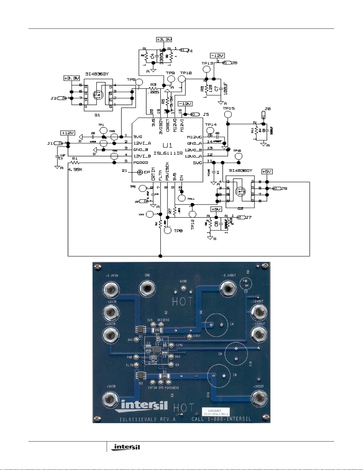
Biasing and General Information
The ISL6111EVAL2 platform (Figure 20) allows a designer to
evaluate and modify the performance and functionality of the
ISL6111 in a simple environment. The board is made such
that the heat dissipating resistors are shielded from users and
equipment by being placed on the bottom, despite this the top
of the load board still gets hot.
Test point names correspond to the ISL6111 device (U1) pins.
Along with the ISL6111 on the ISL6111EVAL2 platform are 2
N-Channel power MOSFETs, (Q1- Q2) these are used as the
external switches for the +5V and +3.3V supplies to the load.
Current sensing is facilitated by the two 5mΩ 1W metal strip
resistors (R7, R3), the voltages developed across the sense
resistors are compared to references on board the ISL6111.
2.74
2.72
2.70
CRTIM LATCH OFF THRESHOLD (V)
2.68
025507585
TEMPERATURE (°C)
TEMPERATURE
Evaluating Current Regulation Duration
The current regulation (CR) duration is set by the CRTIM
capacitor value, C3 to ground. This provides a programmable
duration during which the ISL6111 holds the programmed CR
level. Once this duration has expired and the ISL6111 is still in
CR mode the output voltages will turn off.
The intent of any protection device is to quickly isolate the
voltage supplies so a faulty load card does not drag down a
supply. A duration period too lengthy increases the likelihood
of FET switch damage and results in slower isolation of the
faulty card from the rest of system.
Figures 14 -19 show nominal turn-on, turn-on into OC
condition with CR mode waveforms.
The ISL6111EVAL2 platform is powered through the 5 labeled
jacks on the left half of the board, with outputs on the right
half. After properly biasing the ISL6111, signal the ENABLE
input high (>2.4V), this will turn on the FET switches and
apply voltage to the loads resistors and capacitors.
Voltage and current measurements can be easily made as
the test points facilitate access to IC pins and other critical
circuit nodes.
12

Typical Performance Curves
www.BDTIC.com/Intersil
ISL6111
EN 10V/DIV
CTIM 1V/DIV
4ms/DIV
FIGURE 14. ISL6111 TURN-ON INTO NOMINAL LOAD FIGURE 15. ISL6111 TURN-ON INTO M12V OC CONDITION
M12IOUT 0.1A/DIV CR = 0.12A
12VOUT 5V/DIV
+5VOUT 5V/DIV
+3.3VOUT 5V/DIV
M12VOUT 5V/DIV
EN 10V/DIV
12VOUT 5V/DIV
+5VOUT 5V/DIV
+3.3VOUT 5V/DIV
-12VOUT 5V/DIV
CTIM 1V/DIV
10ms/DIV
12IOUT 0.2A/DIV CR = 0.54A
TIM 5V/DIV
12VOUT 5V/DIV
10ms/DIV
FIGURE 16. M12VOUT INTO CR (VCRSET = 0.461V) FIGURE 17. 12VOUT INTO CR (VCRSET = 0.461V)
3.3IOUT 5A/DIV CR = 10.2A
3VG 2V/DIV
3VSUPPLY 1/DIV
3VOUT 1/DIV
12VOUT 5V/DIV
TIM 5V/DIV
10ms/DIV
5IOUT 5A/DIV CR = 7.2A
5VSUPPLY 2/DIV
5VG 2V/DIV
5VOUT 2/DIV
TIM 5V/DIV
FIGURE 18. 3.3V INTO CR (VCRSET = 0.461V) FIGURE 19. 5VOUT INTO CR (VCRSET = 0.461V)
10ms/DIV
TIM 5V/DIV
13
10ms/DIV
ISL6111
www.BDTIC.com/Intersil
FIGURE 20. ISL6111EVAL2 PLATFORM SCHEMATIC AND PHOTOGRAPH
14

ISL6111
www.BDTIC.com/Intersil
TABLE 3. ISL6111EVAL2 BOARD COMPONENT LISTING
COMPONENT
DESIGNATOR COMPONENT NAME COMPONENT DESCRIPTION
CONTROLLER BOARD
U1 ISL6111CR PCI HotPlug Controller Intersil, ISL6111CR PCI HotPlug Controller
Q1, Q2 Siliconix Si4404DY 4.5mΩ, 30V, 23A Logic Level N-Channel MOSFET or Equivalent
R3, R7 Sense Resistor for 3.3V and 5V Supplies WSL-2512 5mΩ, 1% Metal Strip Resistor or Equivalent
R5 Current Regulation Set Resistor 4.53kΩ 0805 Chip Resistor
C3 Current Regulation Duration Set Capacitor 0.47µF 0805 Chip Capacitor (CR duration ~70ms)
R1, R4 PGOOD , FLTN Pull-up Resistor 5kΩ 0402 Chip Resistor
C1 12VI Decoupling Capacitor 1µF 0603 Chip Capacitor
C6 M12VG Decoupling Capacitor 5600pF 0402 Chip Capacitor
C2, C5 Optional Gate Timing Capacitors NOT POPULATED 0805 Chip Capacitor
R2, R6 3.3V Load Resistor 2.2Ω, 5W
R9, R10 5.0V Load Resistor 5.1Ω, 5W
R11 +12V Load Resistor 47Ω, 5W
R8 -12V Load Resistor 240Ω, 2W
C4, C8 +3.3V and +5.0V Load Capacitors 2200µF
C9 +12V Load Capacitor 330µF
C7 -12V Load Capacitor 100µF
15

ISL6111
www.BDTIC.com/Intersil
Quad Flat No-Lead Plastic Package (QFN)
Micro Lead Frame Plastic Package (MLFP)
L20.5x5
20 LEAD QUAD FLAT NO-LEAD PLASTIC PACKAGE
(COMPLIANT TO JEDEC MO-220VHHC ISSUE C)
MILLIMETERS
SYMBOL
A 0.80 0.90 1.00 -
A1 - - 0.05 -
A2 - - 1.00 9
A3 0.20 REF 9
b 0.23 0.28 0.38 5, 8
D 5.00 BSC -
D1 4.75 BSC 9
D2 2.95 3.10 3.25 7, 8
E 5.00 BSC -
E1 4.75 BSC 9
E2 2.95 3.10 3.25 7, 8
e 0.65 BSC -
k0.25 - - -
L 0.35 0.60 0.75 8
L1 - - 0.15 10
N202
Nd 5 3
Ne 5 3
P- -0.609
θ --129
NOTES:
1. Dimensioning and tolerancing conform to ASME Y14.5-1994.
2. N is the number of terminals.
3. Nd and Ne refer to the number of terminals on each D and E.
4. All dimensions are in millimeters. Angles are in degrees.
5. Dimension b applies to the metallized terminal and is measured
between 0.15mm and 0.30mm from the terminal tip.
6. The configuration of the pin #1 identifier is optional, but must be
located within the zone indicated. The pin #1 identifier may be
either a mold or mark feature.
7. Dimensions D2 and E2 are for the exposed pads which provide
improved electrical and thermal performance.
8. Nominal dimensions are provided to assist with PCB Land Pattern
Design efforts, see Intersil Technical Brief TB389.
9. Features and dimensions A2, A3, D1, E1, P & θ are present when
Anvil singulation method is used and not present for saw
singulation.
10. Depending on the method of lead termination at the edge of the
package, a maximum 0.15mm pull back (L1) maybe present. L
minus L1 to be equal to or greater than 0.3mm.
NOTESMIN NOMINAL MAX
Rev. 3 10/02
All Intersil U.S. products are manufactured, assembled and tested utilizing ISO9000 quality systems.
Intersil Corporation’s quality certifications can be viewed at www.intersil.com/design/quality
Intersil products are sold by description only. Intersil Corporation reserves the right to make changes in circuit design, software and/or specifications at any time without
notice. Accordingly, the reader is cautioned to verify that data sheets are current before placing orders. Information furnished by Intersil is believed to be accurate and
reliable. However, no responsibility is assumed by Intersil or its subsidiaries for its use; nor for any infringements of patents or other rights of third parties which may result
from its use. No license is granted by implication or otherwise under any patent or patent rights of Intersil or its subsidiaries.
For information regarding Intersil Corporation and its products, see www.intersil.com
16
 Loading...