

查询ISL59444供应商
®
ISL59444
Data Sheet September 21, 2005
1GHz, 4 x 1 Multiplexing Amplifier with
Synchronous Controls
The ISL59444 is a single-output 4:1 MUX-amp. The MUX-amp
has a fixed gain of 1 and a 1GHz bandwidth. The ISL59444 is
ideal for professional video switching, HDTV, computer
display routing, and other high performance applications.
The device contains logic inputs for channel selection (S0,
S1), latch control signals (LE1
, LE2), and a three-state
output control (HIZ) for individual selection of MUX amps
that share a common video output line. All logic inputs have
pull-downs to ground and may be left floating.
TABLE 1. TRUTH TABLE
LE1
/LE2 HIZ S1 S0 OUT
0000IN0
0001IN1
0010IN2
0011IN3
X1XXHiZ
Ordering Information
PAR T
NUMBER
ISL59444IB 59444IB 16 Ld SO
ISL59444IB-T7 59444IB 16 Ld SO
ISL59444IB-T13 59444IB 16 Ld SO
ISL59444IBZ
(Note)
ISL59444IBZ-T13
(Note)
ISL59444IBZ-T7
(Note)
†
SO16 (0.150”)
NOTE: Intersil Pb-free plus anneal products employ special Pb-free
material sets; molding compounds/die attach materials and 100%
matte tin plate termination finish, which are RoHS compliant and
compatible with both SnPb and Pb-free soldering operations. Intersil
Pb-free products are MSL classified at Pb-free peak reflow
temperatures that meet or exceed the Pb-free requirements of
IPC/JEDEC J STD-020.
PAR T
MARKING PACKAGE
59444IBZ 16 Ld SO
(Pb-free)
59444IBZ 16 Ld SO
(Pb-free)
59444IBZ 16 Ld SO
(Pb-free)
TAPE &
REEL
†
- MDP0027
†
7” MDP0027
†
13” MDP0027
†
- MDP0027
†
7” MDP0027
†
13” MDP0027
PKG.
DWG. #
Timing Diagram
LE1
LE2
S0, S1, HIZ
OUT
CHX CHY CHZ
CHX
CHY CHX
CHX
CHZ
CHZ
FN7451.1
Features
• 1GHz (-3dB) Bandwidth (V
• 220MHz (-3dB) Bandwidth (V
• Slew Rate (R
• Slew Rate (R
= 500Ω, V
L
= 500Ω, V
L
• High Speed Three-State Output (HIZ)
• Pb-Free Plus Anneal Available (RoHS Compliant)
= 200mV
OUT
= 2V
OUT
= 4V) . . . . . . . . . . . .1515V/µs
OUT
= 5V) . . . . . . . . . . . . 1155V/µs
OUT
P-P
P-P
)
)
Applications
• HDTV/DTV Analog Inputs
• Video Projectors
• Computer Monitors
• Set-top Boxes
• Security Video
• Broadcast Video Equipment
• RGB Video Distribution Systems
• RF Switching and Routing
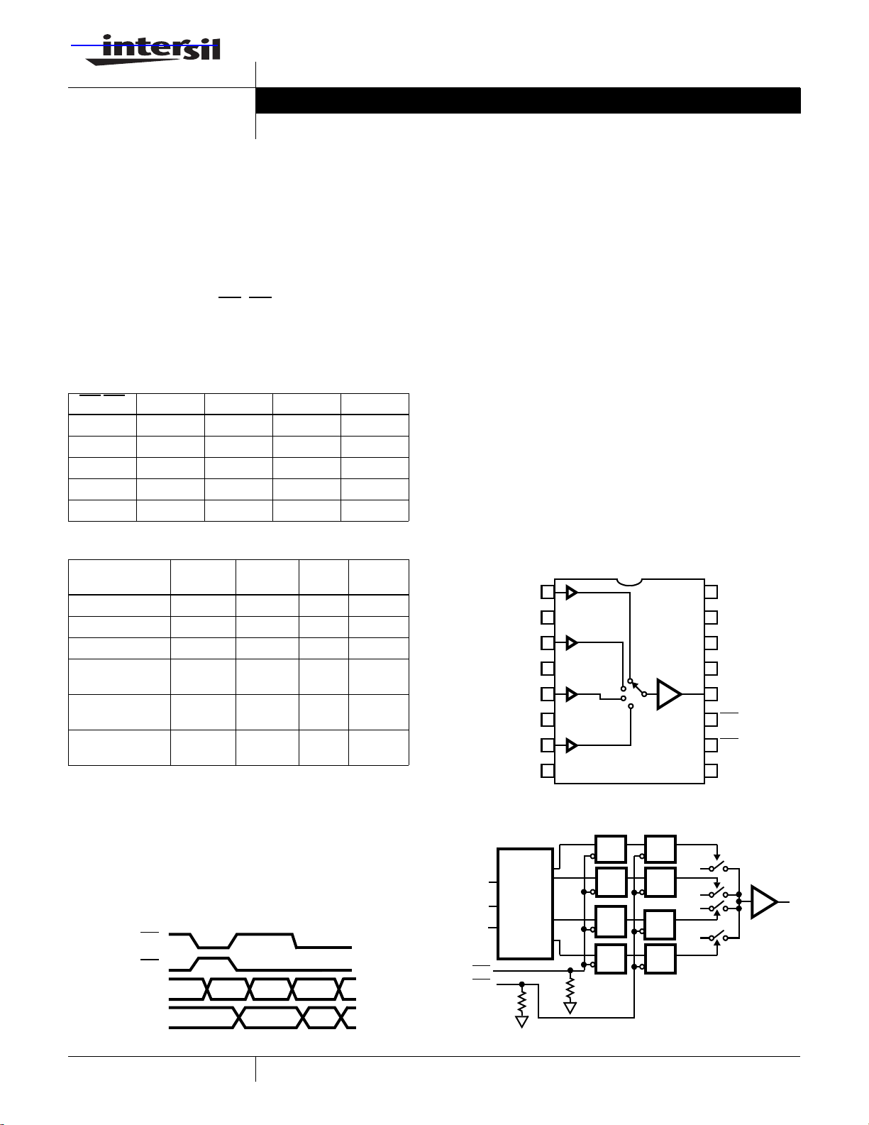
Pinout
IN0
NIC
IN1
GND
IN2
NIC
IN3
ISL59444 (16 LD SO)
TOP VIEW
1
2
3
4
5
6
7
8 9
16
V+
S0
15
S1
14
HIZ
13
OUT
12
LE2
11
LE1
10
V-NIC
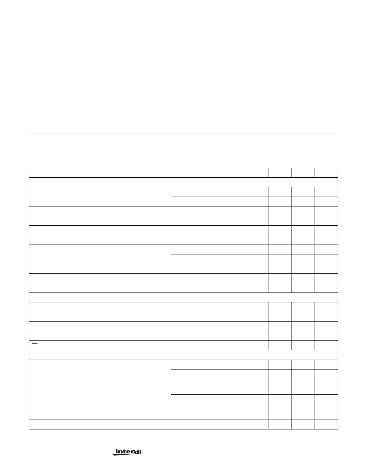
Functional Diagram
EN0
HIZ
LE1
LE2
S0
S1
100kΩ
DECODE
EN1
EN2
EN3
DLQ
C
D
C
D
C
D
C
100kΩ
DLQ
C
Q
L
Q
L
Q
L
IN0
Q
D
L
C
IN1
IN2
Q
D
L
C
IN3
Q
D
L
C
OUT
1
CAUTION: These devices are sensitive to electrostatic discharge; follow proper IC Handling Procedures.
1-888-INTERSIL or 1-888-468-3774
| Intersil (and design) is a registered trademark of Intersil Americas Inc.
All other trademarks mentioned are the property of their respective owners.
Copyright © Intersil Americas Inc. 2005. All Rights Reserved.
ISL59444
Absolute Maximum Ratings (T
Supply Voltage (V+ to V-). . . . . . . . . . . . . . . . . . . . . . . . . . . . . . . 11V
Input Voltage . . . . . . . . . . . . . . . . . . . . . . . . . . . . V- -0.5V, V+ +0.5V
Supply Turn-on Slew Rate . . . . . . . . . . . . . . . . . . . . . . . . . . . 1V/µs
Digital & Analog Input Current (Note 1) . . . . . . . . . . . . . . . . . . 50mA
Output Current (Continuous) . . . . . . . . . . . . . . . . . . . . . . . . . . 50mA
ESD Rating
= 25°C)
A
Storage Temperature Range . . . . . . . . . . . . . . . . . .-65°C to +150°C
Ambient Operating Temperature . . . . . . . . . . . . . . . .-40°C to +85°C
Operating Junction Temperature . . . . . . . . . . . . . . .-40°C to +125°C
Power Dissipation . . . . . . . . . . . . . . . . . . . . . . . . . . . . . See Curves
θ
. . . . . . . . . . . . . . . . . . . . . . . . . . . . . . . . . . . . . . . . . See Curves
JA
Human Body Model (Per MIL-STD-883 Method 3015.7). . . . . . 3kV
Machine Model . . . . . . . . . . . . . . . . . . . . . . . . . . . . . . . . . . .300V
CAUTION: Stresses above those listed in “Absolute Maximum Ratings” may cause permanent damage to the device. This is a stress only rating and operation of the
device at these or any other conditions above those indicated in the operational sections of this specification is not implied.
NOTE:
1. If an input signal is applied before the supplies are powered up, the input current must be limited to these maximum values.
IMPORTANT NOTE: All parameters having Min/Max specifications are guaranteed. Typical values are for information purposes only. Unless otherwise noted, all tests
are at the specified temperature and are pulsed tests, therefore: T
Electrical Specifications V+ = +5V, V- = -5V, GND = 0V, T
Unless Otherwise Specified
= TC = T
J
A
25°C, RL = 500Ω to GND, V
A =
HIZ
= 0.8V,
PARAMETER DESCRIPTION CONDITIONS MIN TYP MAX UNIT
GENERAL
I
Supply Current (V
S
V
I
OUT
V
OUT
OS
Positive and Negative Output Swing VIN = ±3.5V, RL = 500Ω ±3.2 ±3.44 V
Output Current RL = 10Ω to GND ±80 ±120 ±180 mA
Output Offset Voltage -2 9 20 mV
Ib Input Bias Current V
R
out
R
IN
ACL or A
I
TRI
V
Output Resistance HIZ = logic high, (DC), AV = 1 1.4 MΩ
Input Resistance VIN = ±3.5V 10 MΩ
Voltage Gain VIN = ±1.5V, RL = 500Ω 0.999 1.001 1.003 V/V
Output Current in Three-state V
= 0V) No load, V
OUT
= 0.8V 14.5 18 20 mA
HIZ
No load, V
= 0V -5 -2.5 -1 µA
IN
HIZ = logic low, (DC), A
OUT
= 2.0V 12.5 16 18 mA
HIZ
= 1 0.2 Ω
V
= 0V -35 6 +35 µA
LOGIC
V
H
V
L
I
IH
I
IL
t
LE
Input High Voltage (Logic Inputs) 2 V
Input Low Voltage (Logic Inputs) 0.8 V
Input High Current (Logic Inputs) 50 150 µA
Input Low Current (Logic Inputs) -10 5 µA
LE1, LE2 Minimum Pulse Width - 4 - ns
AC GENERAL
-3dB BW -3dB Bandwidth V
0.1dB BW 0.1dB Bandwidth V
dG Differential Gain Error NTSC-7, R
dP Differential Phase Error NTSC-7, R
V
R
V
R
OUT
OUT
S
OUT
OUT
S
= 200mV
= 2V
=25Ω
= 200mV
= 2V
=25Ω
, CL = 1.6pF 1.0 GHz
P-P
, CL = 23.6pF,
P-P
, CL = 1.6pF 80 MHz
P-P
, CL = 23.6pF,
P-P
= 150 0.01 %
L
= 150 0.02 °
L
230 MHz
50 MHz
2
FN7451.1
September 21, 2005
ISL59444
Electrical Specifications V+ = +5V, V- = -5V, GND = 0V, T
Unless Otherwise Specified (Continued)
25°C, RL = 500Ω to GND, V
A =
HIZ
= 0.8V,
PARAMETER DESCRIPTION CONDITIONS MIN TYP MAX UNIT
+SR Slew Rate 25% to 75%, V
R
=500Ω, CL = 23.6pF,
L
R
=25Ω
S
-SR Slew Rate 25% to 75%, V
R
=500Ω, CL = 23.6pF,
L
R
=25Ω
S
OUT
OUT
= 5V,
= 5V,
PSRR Power Supply Rejection Ratio DC, PSRR V+ and V- combined
V
± = ±4.5V to ±5.5V
ISO Channel Isolation f = 10MHz, Ch-Ch X-Talk and Off
Isolation, C
= 1.6pF
L
-50 -57 dB
1515 V/µs
1155 V/µs
75 dB
SWITCHING CHARACTERISTICS
V
GLITCH
Channel-to-Channel Switching Glitch VIN = 0V, CL = 23.6pF, RS=25Ω 38 mV
HIZ Switching Glitch VIN = 0V, CL = 23.6pF, RS=25Ω 175 mV
t
SW-L-H
t
SW-H-L
Channel Switching Time Low to High 1.2V logic threshold to 10%
movement of analog output
Channel Switching Time High to Low 1.2V logic threshold to 10%
movement of analog output
32 ns
29 ns
TRANSIENT RESPONSE
tr, tf Rise & Fall Time, 10% to 90% V
t
S
t
PLH
t
PHL
O
S
0.1% Settling Time V
Propagation Delay - Low to High,
10% to 10%
Propagation Delay- High to Low,
10% to 10%
Overshoot V
V
R
R
V
V
R
V
V
R
V
R
OUT
OUT
S
OUT
S
OUT
OUT
S
OUT
OUT
S
OUT
OUT
S
= 200mV
= 2V
=25Ω
= 2V
=25Ω
= 200mV
= 2V
=25Ω
= 200mV
= 2V
=25Ω
= 200mV
= 2V
=25Ω
, CL = 1.6pF 0.68 ns
P-P
, CL = 23.6pF,
P-P
, CL = 23.6pF,
P-P
, CL = 1.6pF 0.5 ns
P-P
, CL = 23.6pF,
P-P
, CL = 1.6pF 0.54 ns
P-P
, CL = 23.6pF,
P-P
, CL = 1.6pF 8.3 %
P-P
, CL = 23.6pF,
P-P
1.4 ns
6.8 ns
0.85 ns
0.88 ns
15.7 %
P-P
P-P
3
FN7451.1
September 21, 2005
ISL59444
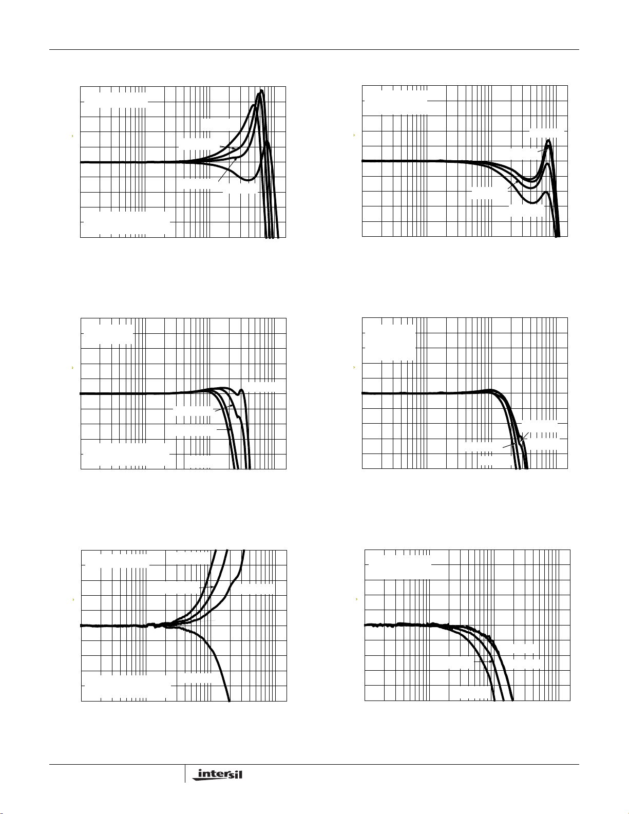
Typical Performance Curves V
5
V
= 200mV
OUT
4
3
2
1
0
-1
-2
NORMALIZED GAIN (dB)
-3
CL INCLUDES 1.6pF
-4
BOARD CAPACITANCE
-5
0.001 0.01 0.1 1
P-P
CL = 7.2pF
CL = 5.5pF
FREQUENCY (GHz)
= ±5V, RL = 500Ω to GND, TA = 25°C, unless otherwise specified.
S
CL = 9.7pF
CL = 1.6pF
FIGURE 1. SMALL SIGNAL GAIN vs FREQUENCY vs C
5
V
= 2V
OUT
4
RS = 25Ω
3
2
1
0
-1
-2
NORMALIZED GAIN (dB)
-3
CL INCLUDES 1.6pF
-4
BOARD CAPACITANCE
-5
0.001 0.01 0.1 1 1.5
P-P
CL = 16.6pF
CL = 23.6pF
CL = 28.6pF
FREQUENCY (MHz)
FIGURE 3. LARGE SIGNAL GAIN vs FREQUENCY vs C
L
CL = 11.6pF
L
1.5
5
V
= 200mV
OUT
4
CL = 1.6pF
3
2
1
0
-1
-2
NORMALIZED GAIN (dB)
-3
-4
-5
0.001 0.01 0.1 1
P-P
RL = 500Ω
RL = 1kΩ
RL = 150Ω
RL = 75Ω
FREQUENCY (MHz)
FIGURE 2. SMALL SIGNAL GAIN vs FREQUENCY vs R
5
V
= 2V
4
OUT
CL = 23.6pF
3
R
2
1
0
-1
-2
NORMALIZED GAIN (dB)
-3
-4
-5
0.001 0.01 0.1 1 1.5
= 25Ω
S
P-P
FREQUENCY (MHz)
RL = 500Ω
RL = 1kΩ
RL = 150Ω
RL = 75Ω
FIGURE 4. LARGE SIGNAL GAIN vs FREQUENCY vs R
1.5
L
L
0.5
V
= 200mV
OUT
0.4
0.3
0.2
0.1
0
-0.1
-0.2
NORMALIZED GAIN (dB)
-0.3
CL INCLUDES 1.6pF
-0.4
BOARD CAPACITANCE
-0.5
0.001 0.01 0.1 1 1.5
P-P
FREQUENCY (MHz)
CL = 9.7pF
CL = 7.2pF
CL = 1.6pF
CL = 5.5pF
FIGURE 5. SMALL SIGNAL 0.1dB GAIN vs FREQUENCY vs C
4
0.5
V
= 200mV
OUT
0.4
CL = 1.6pF
0.3
0.2
0.1
0
-0.1
-0.2
NORMALIZED GAIN (dB)
-0.3
-0.4
-0.5
0.001 0.01 0.1 1 1.5
L
FIGURE 6. SMALL SIGNAL 0.1dB GAIN vs FREQUENCY vs R
P-P
RL = 150Ω
RL = 75Ω
FREQUENCY (MHz)
RL = 1kΩ
RL = 500Ω
September 21, 2005
L
FN7451.1

ISL59444
Typical Performance Curves V
0.2
0.1
0
-0.1
-0.2
-0.3
-0.4
V
= 2V
OUT
-0.5
RS = 25Ω
NORMALIZED GAIN (dB)
-0.6
CL INCLUDES 1.6pF
-0.7
BOARD CAPACITANCE
-0.8
0.001 0.01 0.1 1 1.5
P-P
CL = 16.6pF
CL = 23.6pF
CL = 28.6pF
FREQUENCY (MHz)
= ±5V, RL = 500Ω to GND, TA = 25°C, unless otherwise specified. (Continued)
S
CL = 11.6pF
FIGURE 7. LARGE SIGNAL 0.1dB GAIN vs FREQUENCY vs C
20
VIN = 200mV
10
CL = 23.6pF
0
R
= 25Ω
S
-10
-20
-30
-40
PSRR (dB)
-50
-60
-70
-80
0.3 1 10 100 1000
P-P
PSRR (V+)
PSRR (V-)
FREQUENCY (MHz)
FIGURE 9. PSRR CHANNELS FIGURE 10. CROSSTALK AND OFF ISOLATION
5
V
= 2V
OUT
4
CL = 23.6pF
3
R
2
1
0
-1
-2
NORMALIZED GAIN (dB)
-3
-4
-5
0.001 0.01 0.1 1 1.5
L
FIGURE 8. LARGE SIGNAL 0.1dB GAIN vs FREQUENCY vs R
-10
-20
-30
-40
-50
-60
(dB)
-70
-80
-90
-100
-110
0.001 0.1 10 100 500
P-P
= 25Ω
S
VIN = 1V
P-P
CL = 23.6pF
R
= 25Ω
S
CROSSTALK
OFF ISOLATION
RL = 500Ω
RL = 150Ω
RL = 75Ω
FREQUENCY (MHz)
10.01 3 6
FREQUENCY (MHz)
RL = 1kΩ
L
100
V
= 100mV
OUT
10
1
OUTPUT RESISTANCE (Ω)
0.1
0.1 1 10 100 1000
FIGURE 11. R
P-P
FREQUENCY (MHz)
vs FREQUENCY FIGURE 12. INPUT NOISE vs FREQUENCY
OUT
5
60
50
40
30
20
INPUT VOLTAGE NOISE (nV/√Hz)
10
0
0.1
RF = 500Ω
110100
FREQUENCY (kHz)
FN7451.1
September 21, 2005
ISL59444
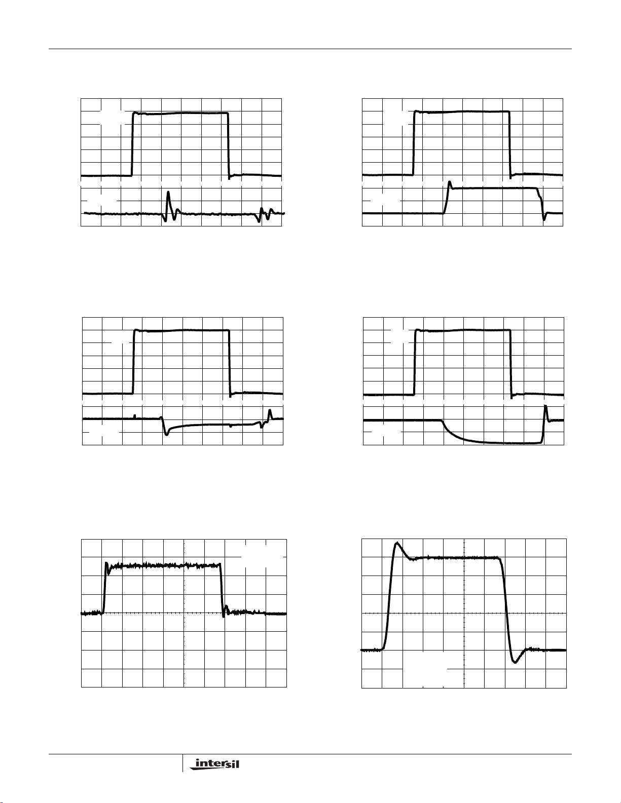
Typical Performance Curves V
S0, S1
1V/DIV20mV/DIV
0
0
V
OUT
20ns/DIV
= ±5V, RL = 500Ω to GND, TA = 25°C, unless otherwise specified. (Continued)
S
FIGURE 13. CHANNEL TO CHANNEL SWITCHING GLITCH
V
=0V, RS= 25, CL = 23.6pF
IN
HIZ
S0, S1
1V/DIV500mV/DIV
0
V
OUT
0
20ns/DIV
FIGURE 14. CHANNEL TO CHANNEL TRANSIENT RESPONSE
=1V, RS= 25, CL = 23.6pF
V
IN
HIZ
1V/DIV
0
0
V
OUT
100mV/DIV
20ns/DIV
FIGURE 15. HIZ SWITCHING GLITCH V
C
= 23.6pF
L
160
120
80
40
0
-40
-80
OUTPUT VOLTAGE (mV)
-120
-160
TIME (4ns/DIV)
= 0V, RS= 25,
IN
CL = 1.6pF
R
= 500Ω
L
1V/DIV
0
V
500mV/DIV
OUT
0
20ns/DIV
FIGURE 16. HIZ TRANSIENT RESPONSE V
C
= 23.6pF
L
2.4
2
1.6
1.2
0.8
0.4
OUTPUT VOLTAGE (V)
0
-0.4
-0.8
CL = 23.6pF
R
= 25Ω
S
= 500Ω
R
L
TIME (4ns/DIV)
= 1V, RS= 25,
IN
FIGURE 17. SMALL SIGNAL TRANSIENT RESPONSE FIGURE 18. LARGE SIGNAL TRANSIENT RESPONSE
6
FN7451.1
September 21, 2005

ISL59444
Typical Performance Curves V
JEDEC JESD51-7 HIGH EFFECTIVE THERMAL
CONDUCTIVITY TEST BOARD
1.4
1.250W
1.2
1
0.8
0.6
0.4
POWER DISSIPATION (W)
0.2
0
0 25 50 75 100 150
FIGURE 19. PACKAGE POWER DISSIPATION vs AMBIENT
TEMPERATURE
S
O
1
6
θ
(
J
0
A
.
=8
1
5
0
0
°
”
C
)
/
W
AMBIENT TEMPERATURE (°C)
= ±5V, RL = 500Ω to GND, TA = 25°C, unless otherwise specified. (Continued)
S
JEDEC JESD51-3 LOW EFFECTIVE THERMAL
CONDUCTIVITY TEST BOARD
1
0.9
909mW
0.8
0.7
0.6
0.5
0.4
0.3
0.2
POWER DISSIPATION (W)
0.1
12585
0
0 25 50 75 100 150
S
O
1
θ
6
J
(
0
A
=
.
1
1
5
1
0
0
”
°
)
C
/
W
AMBIENT TEMPERATURE (°C)
FIGURE 20. PACKAGE POWER DISSIPATION vs AMBIENT
TEMPERATURE
Pin Descriptions
EQUIVALENT
PIN NUMBER PIN NAME
1 IN0 Circuit 1 Input for channel 0
2, 6, 8 NIC Not Internally Connected; it is recommended this pin be tied to ground to minimize
3 IN1 Circuit 1 Input for channel 1
4 GND Circuit 4 Ground pin
5 IN2 Circuit 1 Input for channel 2
7 IN3 Circuit 1 Input for channel 3
9 V - Circuit 4 Negative Power Supply
10 LE1
11 LE 2
12 OUT Circuit 3 Output
13 HIZ Circuit 2 Output disable (active high); there are internal pull-down resistors, so the device will be
14 S1 Circuit 2 Channel selection pin MSB (binary logic code)
15 S0 Circuit 2 Channel selection pin LSB (binary logic code)
16 V+ Circuit 4 Positive power supply
CIRCUIT DESCRIPTION
crosstalk.
Circuit 2 Synchronized channel switching: When LE1 is low, the master control latch loads the
next switching address. The Mux Amp is configured for this address when LE2
Synchronized operation results when LE2
asynchronous (changes with any control signal change) if both LE1
is the inverse of LE1. Channel selection is
and LE2 are both
low.
Circuit 2 Synchronized channel switching: When LE2 is low, the newly selected channel, stored
in the master latch via LE1
inverse of LE1
. Channel selection is asynchronous (changes with any control signal
change) if both LE1
is selected. Synchronized operation results when LE2 is the
and LE2 are both low.
active with no connection; "HI" puts the output in high impedance state.
12585
goes low.
7
FN7451.1
September 21, 2005

Pin Descriptions (Continued)
V
PIN NUMBER PIN NAME
ISL59444
EQUIVALENT
CIRCUIT DESCRIPTION
+
V+
IN
CIRCUIT 1 CIRCUIT 2
CIRCUIT 3
AC Test Circuits
V
IN
50Ω
or
75Ω
ISL59444
C
2pF
V+
OUT
V-
L
21k
LOGICPIN
33k
V-
V+
GND
V-
+
1.2V
-
CAPACITIVELY
COUPLED
ESD CLAMP
GND.
V-
CIRCUIT 4
R
L
500Ω
ISL59444
V
IN
50Ω
or
75Ω
C
2pF
L
R
475Ω
S
50Ω
or
75Ω
TEST
EQUIPMENT
50Ω
or
75Ω
FIGURE 21A. TEST CIRCUIT WITH OPTIMAL OUTPUT LOAD FIGURE 21B. TEST CIRCUIT FOR MEASURING WITH A 50Ω OR
75Ω INPUT TERMINATED EQUIPMENT
ISL59444
V
IN
50Ω
or
75Ω
R
50Ω or 75Ω
C
L
2pF
S
FIGURE 21C. BACKLOADED TEST CIRCUIT FOR VIDEO CABLE APPLICATION. BANDWIDTH AND LINEARITY FOR R
TEST
EQUIPMENT
50Ω
or
75Ω
LESS THAN 500Ω
L
WILL BE DEGRADED.
Figure 21A illustrates the optimum output load for testing AC performance. Figure 21B illustrates the optimum output load when
connecting to input terminated equipment. Figure 21C illustrates back loaded test circuit for video cable.
8
FN7451.1
September 21, 2005
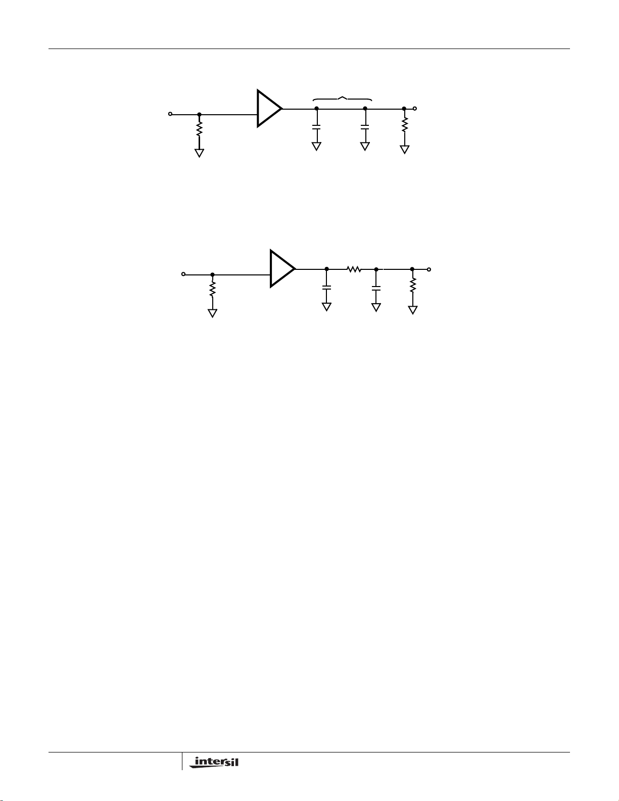
Application Circuits
V
ISL59444
*C
= CT + C
L
-
IN
50Ω
FIGURE 22A. SMALL SIGNAL 200mV
V
IN
50Ω
+
-
+
C
1.6pF
1.6pF
OUT
C
T
APPLICATION CIRCUIT
P-P
C
T
OUT
0pF
*CL: TOTAL LOAD CAPACITANCE
C
: TRACE CAPACITANCE
T
C
: OUTPUT CAPACITANCE
OUT
R
S
25Ω
C
OUT
22pF
V
OUT
RL = 500Ω
V
R
= 500Ω
L
OUT
FIGURE 22B. LARGE SIGNAL 1V
Application Information
General
The ISL59444 is a 4:1 mux that is ideal as a matrix element
in high performance switchers and routers. The ISL59444 is
optimized to drive a 2pF in parallel with a 500Ω load. The
capacitance can be split between the PCB capacitance an
and external load capacitance. Their low input capacitance
and high input resistance provide excellent 50Ω or 75Ω
terminations.
Capacitance at the Output
The output amplifier is optimized for capacitance to ground
(C
) directly on the output pin. Increased capacitance
L
causes higher peaking with an increase in bandwidth. The
optimum range for most applications is ~1.0pF to ~6pF. The
optimum value can be achieved through a combination of
PC board trace capacitance (C
(C
. A good method to maintain control over the output
OUT)
pin capacitance is to minimize the trace length (C
next component, and include a discrete surface mount
capacitor (C
) directly at the output pin.
OUT
For large signal applications where overshoot is important
the circuit in Figure 22B should be used. The series resistor
(R
) and capacitor (CL) form a low pass network that limits
S
system bandwidth and reduces overshoot. The component
values shown result in a typical pulse response shown in
Figure 18.
) and an external capacitor
T
) to the
T
CL = CT + C
APPLICATION CIRCUIT
P-P
OUT
Ground Connections
For the best isolation and crosstalk rejection, the GND pin
and NIC pins must connect to the GND plane. The NIC pins
are placed on both sides of the input pins. These pins are
not internally connected to the die. It is recommended this
pin be tied to ground to minimize crosstalk.
Control Signals
S0, S1, HIZ - These pins are, TTL/CMOS compatible control
inputs. The S0, S1 pins select which one of the inputs
connect to the output. The HIZ pin is used to three-state the
output amplifiers. For control signal rise and fall times less
than 10ns the use of termination resistors close to the part
will minimize transients coupled to the output.
HIZ State
An internal pull-down resistor connected to the HIZ pin
ensures the device will be active with no connection to the
HIZ pin. The HIZ state is established within approximately
30ns by placing a logic high (>2V) on the HIZ pin. If the HIZ
state is selected, the output is a high impedance 1.4MΩ. Use
this state to control the logic when more than one mux
shares a common output.
In the HIZ state the output is three-stated, and maintains its
high Z even in the presence of high slew rates. The supply
current during this state is basically the same as the active
state.
9
FN7451.1
September 21, 2005

ISL59444
Latch State
The latched control signals allow for synchronized channel
switching. When LE1
is low the master control latch loads the
next switching address (S0, S1), while the closed (assuming
LE2
is the inverse of LE1) slave control latch maintains the
current state. LE2
switching low closes the master latch (with
previous assumption), loads the now open slave latch, and
switches the crosspoint to the newly selected channel. Channel
selection is asynchronous (changes with any control signal
change) if both LE1
and LE2 are low.
Power-Up Considerations
The ESD protection circuits use internal diodes from all pins
the V+ and V- supplies. In addition, a dv/dt triggered clamp is
connected between the V+ and V- pins, as shown in the
Equivalent Circuits 1 through 4 section of the Pin Description
table. The dv/dt triggered clamp imposes a maximum supply
turn-on slew rate of 1V/µs. Damaging currents can flow for
power supply rates-of-rise in excess of 1V/µs, such as
during hot plugging. Under these conditions, additional
methods should be employed to ensure the rate of rise is not
exceeded.
Consideration must be given to the order in which power is
applied to the V+ and V- pins, as well as analog and logic
input pins. Schottky diodes (Motorola MBR0550T or
equivalent) connected from V+ to ground and V- to ground
(Figure 23) will shunt damaging currents away from the
internal V+ and V- ESD diodes in the event that the V+
supply is applied to the device before the V- supply.
If positive voltages are applied to the logic or analog video
input pins before V+ is applied, current will flow through the
internal ESD diodes to the V+ pin. The presence of large
decoupling capacitors and the loading effect of other circuits
connected to V+, can result in damaging currents through
the ESD diodes and other active circuits within the device.
Therefore, adequate current limiting on the digital and
analog inputs is needed to prevent damage during the time
the voltages on these inputs are more positive than V+.
Limiting the Output Current
No output short circuit current limit exists on these parts. All
applications need to limit the output current to less than
50mA. Adequate thermal heat sinking of the parts is also
required.
PC Board Layout
The frequency response of this circuit depends greatly on
the care taken in designing the PC board. The following are
recommendations to achieve optimum high frequency
performance from your PC board.
• The use of low inductance components such as chip
resistors and chip capacitors is strongly recommended.
• Minimize signal trace lengths. Trace inductance and
capacitance can easily limit circuit performance. Avoid
sharp corners, use rounded corners when possible. Vias
in the signal lines add inductance at high frequency and
should be avoided. PCB traces greater than 1" begin to
exhibit transmission line characteristics with signal rise/fall
times of 1ns or less. High frequency performance may be
degraded for traces greater than one inch, unless strip
lines are used.
• Match channel-channel analog I/O trace lengths and
layout symmetry. This will minimize propagation delay
mismatches.
• Maximize use of AC de-coupled PCB layers. All signal I/O
lines should be routed over continuous ground planes (i.e.
no split planes or PCB gaps under these lines). Avoid vias
in the signal I/O lines.
• Use proper value and location of termination resistors.
Termination resistors should be as close to the device as
possible.
• When testing use good quality connectors and cables,
matching cable types and keeping cable lengths to a
minimum.
• Minimum of 2 power supply de-coupling capacitors are
recommended (1000pF, 0.01µF) as close to the devices
as possible. Avoid vias between the cap and the device
because vias add unwanted inductance. Larger caps can
be farther away. When vias are required in a layout, they
should be routed as far away from the device as possible.
• The NIC pins are placed on both sides of the input pins.
These pins are not internally connected to the die. It is
recommended these pins be tied to ground to minimize
crosstalk.
V+ SUPPLY
LOGIC
POWER
GND
SIGNAL
DE-COUPLING
V- SUPPLY
CAPS
10
SCHOTTKY
PROTECTION
V+
S0
V-
GND
IN0
IN1
FIGURE 23. SCHOTTKY PROTECTION CIRCUIT
V+
V-
V+
V-
V+
CONTROL
V-
LOGIC
V+
OUT
V-
EXTERNAL
CIRCUITS
September 21, 2005
FN7451.1

SO Package Outline Drawing
ISL59444
NOTE: The package drawing shown here may not be the latest version. To check the latest revision, please refer to the Intersil website at
<http://www.intersil.com/design/packages/index.asp>
All Intersil U.S. products are manufactured, assembled and tested utilizing ISO9000 quality systems.
Intersil Corporation’s quality certifications can be viewed at www.intersil.com/design/quality
Intersil products are sold by description only. Intersil Corporation reserves the right to make changes in circuit design, software and/or specifications at any time without
notice. Accordingly, the reader is cautioned to verify that data sheets are current before placing orders. Information furnished by Intersil is believed to be accurate and
reliable. However, no responsibility is assumed by Intersil or its subsidiaries for its use; nor for any infringements of patents or other rights of third parties which may result
from its use. No license is granted by implication or otherwise under any patent or patent rights of Intersil or its subsidiaries.
For information regarding Intersil Corporation and its products, see www.intersil.com
11
FN7451.1
September 21, 2005
 Loading...