Intersil ISL5640 Datasheet

ISL5640
ADVANCE INFORMATION
Data Sheet June 2000
3V Dual 8-Bit, 20/40/60MSPS A/D
Converter with Internal Voltage Reference
The ISL5640 is a monolithic, dual 8-bit analog-to-digital
converter fabricated in an advanced CMOS process. It is
designed for high speed applications where integration,
bandwidth and accuracy are essential. The ISL5640
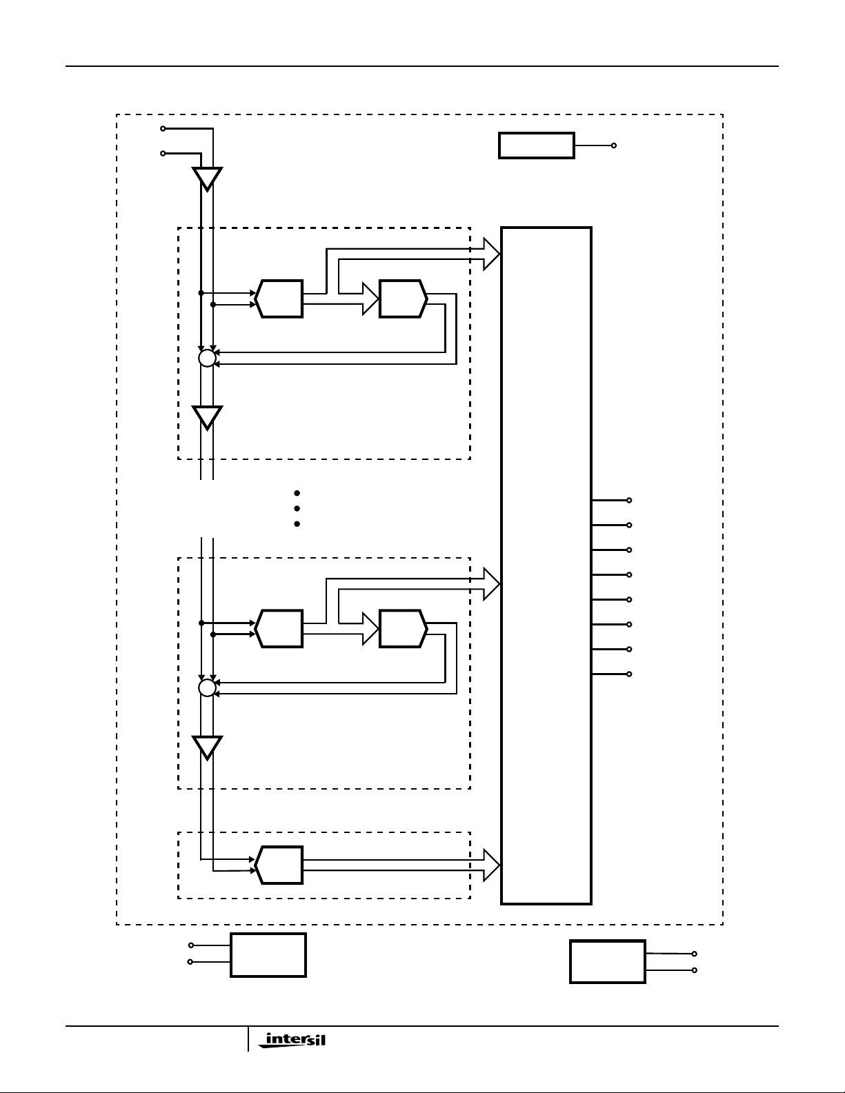
features a 9-stage pipeline architecture. The fully pipelined
architecture and an innovative input stage enable the
ISL5640 to accept a variety of input configurations, singleended or fully differential. Only one external clock is
necessary to drivebothconverters and an internal band-gap
voltage reference is provided. This allows the system
designer to realize an increased level of system integration
resulting in decreased cost and power dissipation.
The ISL5640 has excellent dynamic performance while
consuming less than 100mW power at 40MSPS. The A/D
only requires a single +3.0V power supply. Data output
latches are provided which present valid data to the output
bus with a latency of 5 clock cycles.
File Number 4657.3
Features
• Sampling Rate . . . . . . . . . . . . . . . . . . . . . . . . . . .40MSPS
• 7.4 Bits at f
• Low Power at 40MSPS. . . . . . . . . . . . . . . . . . . . . 100mW
• Power Down Mode . . . . . . . . . . . . . . . . . . . . . . . . . <1mW
• Wide Full Power Input Bandwidth. . . . . . . . . . . . . 250MHz
• SFDR at f
• Excellent Channel-to-Channel Isolation. . . . . . . . . >75dB
• On-Chip Sample and Hold Amplifiers
• Internal Bandgap Voltage Reference . . . . . . . . . . . . 1.25V
• Single Supply Voltage Operation . . . . . . . . . . . . . . . +3.0V
• Offset Binary or Two’s Complement Output Format
• Dual 8-Bit A/D Converters on a Monolithic Chip
• Pin Compatible Upgrade to AD9288
= 1MHz
IN
= 1MHz. . . . . . . . . . . . . . . . . . . . . . . . . .55dB
IN
The ISL5640 is offered in 20MSPS, 30MSPS, 40MSPS and
60MSPS sampling rates.
Ordering Information
TEMP.
PART
NUMBER
RANGE
(oC) PACKAGE PKG. NO.
ISL5640/2IN -40 to 85 48 Ld LQFP Q48.7x7 20
ISL5640/3IN -40 to 85 48 Ld LQFP Q48.7x7 30
ISL5640/4IN -40 to 85 48 Ld LQFP Q48.7x7 40
ISL5640/6IN -40 to 85 48 Ld LQFP Q48.7x7 60
ISL5640 EVAL 25 Evaluation Platform
SAMPLING
RATE
(MSPS)
Applications
• Wireless Local Loop
• PSK and QAM I&Q Demodulators
• Medical Imaging
• High Speed Data Acquisition
Pinout
48 LEAD LQFP
TOP VIEW
CC
CC
IV
V
ROUT
QV
GND
I
IN
I
IN
DFS
RIN
RIN
S1
S2
Q
IN
QIN+
GND
DV
I CLK
AV
1
+
-
-
2
3
4
5
6
7
8
9
10
11
12
13 14 15 16
GND
ID7
ID6
ID5
ID4
ID3
ID2
ID1
ID0
373839404142434445464748
36
35
34
33
32
31
30
29
28
27
26
25
2423222120191817
N/C
N/C
GND
DV
GND
AV
AV
GND
DV
GND
N/C
N/C
CC
CC
CC
CC
3-1
CC
CC
AV
CAUTION: These devices are sensitive to electrostatic discharge; follow proper IC Handling Procedures.
1-888-INTERSIL or 321-724-7143
DV
Q CLK
GND
QD5
QD7
QD6
QD4
QD3
QD2
QD1
QD0
| Copyright © Intersil Corporation 2000

Functional Block Diagram
-
I/Q
IN
I/Q
+
IN
S/H
STAGE 1
ISL5640
CLOCK
I/QCLK
2-BIT
FLASH
+
-
∑
X2
STAGE 8
2-BIT
FLASH
+
∑
-
2-BIT
DAC
2-BIT
DAC
DIGITAL DELAY
AND
DIGITAL ERROR
CORRECTION
I/QD7 (MSB)
I/QD6
I/QD5
I/QD4
I/QD3
I/QD2
I/QD1
I/QD0 (LSB)
V
I/QV
ROUT
RIN
X2
REFERENCE
3-2
2-BIT
FLASH
STAGE 9
AV
CC
AGND DV
CC
DGND
I OR Q CHANNEL
MODE
DATA FORMAT
S1/S2
DFS

Typical Application Schematic
ISL5640
ISL5640
+
I
IN
- (3) IIN-
I
IN
QIN+
QIN-
0.1µF
(2) I
+
IN
(11) QIN+
(10) QIN-
(5) IV
RIN
(6) QV
RIN
(7) V
ROUT
ID1 (38)
ID2 (39)
ID3 (40)
ID4 (31)
ID5 (42)
ID6 (43)
(MSB) ID7 (44)
(LSB) QD0 (24)
QD1 (23)
QD2 (22)
QD3 (21)
QD4 (20)
QD5 (19)
QD6 (18)
(MSB) QD7 (17)
ICLK (47)
QCLK (14)
ID0(LSB) ID0 (37)
ID1
ID2
ID3
ID4
ID5
ID6
ID7
QD0
QD1
QD2
QD3
QD4
QD5
QD6
QD7
CLOCK
+3V
10µF
S1 (8)
S2 (9)
DFS (4)
AGND
(13,30,31,48) AV
(12,29,32) AGND
DGND
+
0.1µF
BNC
CC
DVCC(15, 28, 33, 46)
DGND (16, 27, 34, 45)
10µF AND 0.1µF CAPS
ARE PLACED AS CLOSE
TO PART AS POSSIBLE
S1
S2
DFS
0.1µF10µF
+
3V
3-3

ISL5640
Pin Descriptions
PIN NO. NAME DESCRIPTION
1A
2I
3I
GND
IN+
IN-
4 DFS Data Format Select (Low for Offset
5IV
6V
RIN
ROUT
7QV
8 S1 Mode Select Pin 1 (See Table)
9 S2 Mode Select Pin 2 (See Table)
10 Q
11 Q
12 A
IN+
GND
13 AV
14 QCLK Q-Channel Clock Input
15 DV
16 D
GND
17 QD7 Q-Channel, Data Bit 7 Output (MSB)
18 QD6 Q-Channel, Data Bit 6 Output
19 QD5 Q-Channel, Data Bit 5 Output
20 QD4 Q-Channel, Data Bit 4 Output
21 QD3 Q-Channel, Data Bit 3 Output
22 QD2 Q-Channel, Data Bit 2 Output
23 QD1 Q-Channel, Data Bit 1 Output
Analog Ground
I-Channel Positive Analog Input
I-Channel Negative Analog Input
Binary and High for Twos Complement
Output Format)
I-Channel Voltage Reference Input
+1.25V Reference Voltage Output
(Decouple with 0.1µF Capacitor)
Q-Channel Voltage Reference Input
RIN
Q-Channel Negative Analog Input
IN-
Q-Channel Positive Analog Input
Analog Ground
Analog Supply
CC
Digital Supply
CC
Digital Ground
Pin Descriptions (Continued)
PIN NO. NAME DESCRIPTION
24 QD0 Q-Channel, Data Bit 0 Output (LSB)
25 N/C No Connect
26 N/C No Connect
27 D
GND
28 DV
29 A
GND
30 AV
31 AV
32 A
GND
33 DV
34 D
GND
35 N/C No Connect
36 N/C No Connect
37 ID0 I-Channel, Data Bit 0 Output
38 ID1 I-Channel, Data Bit 1 Output
39 ID2 I-Channel, Data Bit 2 Output
40 ID3 I-Channel, Data Bit 3 Output
41 ID4 I-Channel, Data Bit 4 Output
42 ID5 I-Channel, Data Bit 5 Output
43 ID6 I-Channel, Data Bit 6 Output
44 ID7 I-Channel, Data Bit 7 Output (MSB)
45 D
GND
46 DV
47 ICLK I-Channel Clock Input
48 AV
CC
CC
CC
CC
CC
CC
Digital Ground
Digital Supply
Analog Ground
Analog Supply
Analog Supply
Analog Ground
Digital Supply
Digital Ground
Digital Ground
Digital Supply
Analog Supply
3-4
 Loading...