

Page 1
®
www.BDTIC.com/Intersil
ISL5585
Data Sheet October 21, 2004
3.3V Ringing SLIC Family for Voice Over
Broadband (VOB)
The 3.3V family of ringing subscriber line interface circuits
(SLIC) supports analog Plain Old T elephone Service (POTS)
in short and medium loop length, wireless and wireline voice
over broadband applications. Ideally suited for customer
premise equipment, this family of products offers flexibility to
designers with high ringing voltage and low power
consumption system requirements.
The ISL5585 family is capable of operating with 100V ringing
battery supply, which translates directly to the amount of
ringing voltage supplied to the subscriber. With the high
operating voltage, subscriber loop lengths can be extended
to 500Ω (i.e., 5,000 feet) and beyond, allowing this family to
serve emerging Fiber In The Loop (FITL) markets.
Other key features across the product family include: 3.3V
V
operation, low power consumption, ringing using
CC
sinusoidal or trapezoidal waveforms, robust auto-detection
mechanisms for when subscribers go on or off hook, and
minimal external discrete application components.
Integrated test access features are also offered on selected
products to support loopback testing as well as line
measurement tests.
There are ten product offerings of the ISL5585 providing
various grades of ringing battery voltage and longitudinal
balance.
FN6026.6
Features
•3.3V Operation
• Onboard Ringing Generation
• Low Standby P ower Consumption (75V, 65mW)
• Programmable Transient Current Limit
• Improved Off Hook Software Interface
• Integrated MTU DC Characteristics
• Low External Component Count
• Silent Polarity Reversal
• Pulse Metering and On Hook Transmission
• Tip Open Ground Start Operation
• Balanced and Unbalanced Ringing
• Thermal Shutdown with Alarm Indicator
• 28 Lead Surface Moun t Packag i n g
• QFN Package:
- Compliant to JEDEC PUB95 MO-220
QFN - Quad Flat No Leads - Package Outline
- Near Chip Scale Package footprint, which improves
PCB efficiency and has a thinner profile
• Pb-Free Available (RoHS Compliant)
Applications
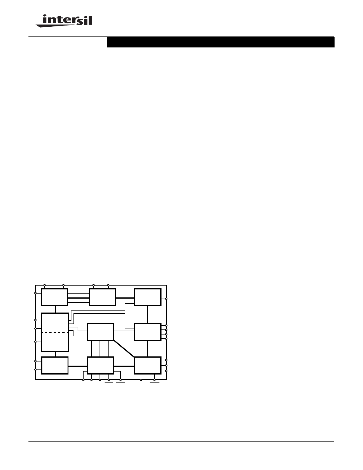
Block Diagram
POL CDC VBHVBL
ILIM
TIP
RING
TL
SW+
SW-
DC
CONTROL
2-WIRE
PORT
TRANSIENT
CURRENT
LIMIT
TEST
ACCESS
BATTERY
SWITCH
TRANSMIT
SENSING
DETECTOR
LOGIC
RT DET
SH E0
ALM
RINGING
PORT
4-WIRE
PORT
CONTROL
LOGIC
BSEL SWC
VRS
AUX
VTX
-IN
VFB
F2
F1
F0
• Short Loop Access Platforms
• Voice Over Internet Protocol (VoIP)
• Voice Over Cable and DSL Modems
• Internet Protocol PBX
• FiberTo The Home (FTTH)
• Remote Subscriber Units
• Ethernet Terminal Adapters
Related Literature
• AN1038, User’s Guide for De velopment Board
• AN9824, Modeling of the AC Loop
• TB379 Thermal Characterization of Packages for ICs
• AN9922, Thermal Characterization and Modeling of the
RSLIC18 in the Micro Leadframe Package
1
CAUTION: These devices are sensitive to electrostatic discharge; follow proper IC Handling Procedures.
1-888-INTERSIL or 321-724-7143
| Intersil (and design) is a registered trademark of Intersil Americas Inc.
All other trademarks mentioned are the property of their respective owners.
Copyright Intersil Americas Inc. 2002-2004. All Rights Reserved.
Page 2

ISL5585
www.BDTIC.com/Intersil
Ordering Information
LONGITUDINAL
HIGH BATTERY (VBH)
PART NUMBER
ISL5585AIM
ISL5585AIMZ
(See Note)
ISL5585BIM
ISL5585BIMZ
(See Note)
ISL5585CIM
ISL5585CIMZ
(See Note)
ISL5585DIM
ISL5585DIMZ
(See Note)
ISL5585ECM
ISL5585ECMZ
(See Note)
ISL5585ECR
ISL5585ECRZ
(See Note)
ISL5585FCM
ISL5585FCMZ
(See Note)
ISL5585FCR
ISL5585FCRZ
(See Note)
ISL5585GCM
ISL5585GCMZ
(See Note)
ISL5585GCR
ISL5585GCRZ
(See Note)
ISL5585 XXX Evaluation board platform, including CODEC.
Also available in Tape and Reel
*Reference “Special Considerations for the QFN Package” text.
NOTE: Intersil Pb-free products employ special Pb-free material sets; molding compounds/die attach materials and 100% matte tin plate termination
finish, which are RoHS compliant and compatible with both SnPb and Pb-free soldering operations. Intersil Pb-free products are MSL classified at Pbfree peak reflow temperatures that meet or exceed the Pb-free requirements of IPC/JEDEC J STD-020C.
•••
•••
•• •
•• •
•••
•••
•••
•••
••
••
••
••
•••
•••
•••
•••
•••
•••
•••
•••
BALANCE
FULL
TEST
TEMP.
RANGE (°C) PACKAGE PKG. DWG. #100V 85V 75V 58dB 53dB
-40 to 85 28 Ld PLCC N28.45
-40 to 85 28 Ld PLCC
(Pb-free)
-40 to 85 28 Ld PLCC N28.45
-40 to 85 28 Ld PLCC
(Pb-free)
-40 to 85 28 Ld PLCC N28.45
-40 to 85 28 Ld PLCC
(Pb-free)
-40 to 85 28 Ld PLCC N28.45
-40 to 85 28 Ld PLCC
(Pb-free)
0 to 75 28 Ld PLCC N28.45
0 to 75 28 Ld PLCC
(Pb-free)
0 to 75 32 Pad QFN L32.7x7*
0 to 75 32 Pad QFN
(Pb-free)
0 to 85 28 Ld PLCC N28.45
0 to 85 28 Ld PLCC
(Pb-free)
0 to 85 32 Pad QFN L32.7x7*
0 to 85 32 Pad QFN
(Pb-free)
0 to 85 28 Ld PLCC N28.45
0 to 85 28 Ld PLCC
(Pb-free)
0 to 85 32 pad QFN L32.7x7*
0 to 85 32 pad QFN
(Pb-free)
N28.45
N28.45
N28.45
N28.45
N28.45
L32.7x7*
N28.45
L32.7x7*
N28.45
L32.7x7*
2
Page 3
ISL5585
www.BDTIC.com/Intersil
Device Operating Modes
MODE F2 F1 F0 E0 = 1 E0 = 0 ISL5585A ISL5585B ISL5585C ISL5585D ISL5585E ISL5585F ISL5585G
Low Power Standby 0 0 0 SHD GKD
Forward Active 0 0 1 SHD GKD
Unbalanced Ringing 0 1 0 RTD RTD
Reverse Active 0 1 1 SHD GKD
Ringing 1 0 0 RTD RTD
Forward Loop Back 1 0 1 SHD GKD
Tip Open 1 1 0 SHD GKD
Power Denial 1 1 1 n/a n/a
•••••••
•••••••
•••••••
•••••••
•••• ••
•••• ••
•••••••
•
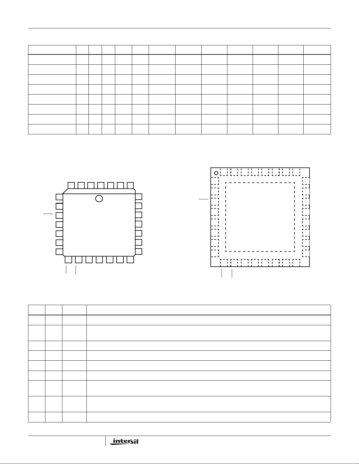
Pinouts
ISL5585 (PLCC)
ISL5585 QFN
TOP VIEW
TOP VIEW
SW+
SW-
SWC
F2
F1
F0
E0
BL
BH
V
V
5
6
7
8
9
10
11
12 13 14 15 16 17 18
DET
ALM
BGND
AGND
TIP
1234
BSEL
RING
TL
SH
POL
VBHVBLBGND
32 31 30 29 28 27 26 25
ILIM
262728
RT
25
24
CDC
23
V
CC
22
-IN
VFB
21
VTX
20
19
AUX
VRS
SW+
1
SW-
2
SWC
3
F2
4
F1
5
F0
6
E0
7
NC
8
910111213141516
DET
ALM
TIP
NC
RING
SCC
SH
24
23
22
21
20
19
18
17
TL
BSEL
AGND
POL
VRS
NC
Pin Description
PLCC QFN SYMBOL DESCRIPTION
1 29 TIP TIP power amplifier output.
2 30 BGND Battery Ground - To be connected to zero potential. All loop current and longitudinal current flow from this ground.
Internally separate from AGND. This ground must be connected to the same potential as AGND.
3 31 VBL Low battery supply connection.
ILIM
RT
CDC
VCC
-IN
VFB
VTX
AUX
4 32 VBH High battery supply connection for the most negative battery.
5 1 SW+ Uncommitted switch positive terminal.
6 2 SW- Uncommitted switch negative terminal.
7 3 SWC Switch control input. This TTL compatible input controls the uncommitted switch, with a logic “0” enabling the switch
and logic “1” disabling the switch.
8 4 F2 Mode Control Input - MSB. F2-F0 for the TTL compatible parallel control interface for controlling the various modes of
operation of the device.
9 5 F1 Mode control input.
3
Page 4

ISL5585
www.BDTIC.com/Intersil
Pin Description (Continued)
PLCC QFN SYMBOL DESCRIPTION
10 6 F0 Mode control input.
11 7 E0 Detector Output Selection Input. This TTL input controls the multiplexing of the SHD (E0 = 1) and GKD (E0 = 0)
comparator outputs to the DET output based upon the state at the F2-F0 pins (see the Device Operating Modes table
shown on page 2).
12 9 DET Detector Output - This TTL output provides on-hook/off-hook status of the loop based upon the selected operating
13 10 ALM Thermal Shutdown Alarm. This pin signals the internal die temperature has exceeded safe operating temperature
14 11 AGND Analog ground reference. This pin should be externally connected to BGND.
15 12 BSEL Selects between high and low battery, with a logic “1” selecting the high battery and logic “0” the low battery.
16 13 TL Programming pin for the transient current limit feature, set by an external resistor to ground.
17 14 POL External capacitor on this pin sets the polarity reversal time.
18 15 VRS Ringing Signal Input - Analog input for driving 2-wire interface while in Ring Mode.
19 17 AUX Auxiliary input - Float if not used.
20 18 VTX Transmit Output V oltage - Output of impedance matching amplifier, AC couples through a resistor to CODEC.
21 19 VFB Feedback voltage for impedance matching. This voltage is scaled to accomplish impedance matching. The CFB
22 20 -IN Analog Receive Voltage - 4-wire analog audio input voltage. connects to CODEC via receive gain setting resistor R
23 21 VCC Positive voltage power supply,+3.3V
24 22 CDC DC Biasing Filter Capacitor - Connects between this pin and V
25 23 RT Ring trip filter network.
mode. The detected output will either be switch hook, ground key or ring trip (see the Device Operating Modes table
shown on page 2). DET
logic state.
(approximately 175°C) and the device has been powered down automatically.
capacitor connects between this pin and the -IN pin. The CFB cap needs to be non-polarized for proper device
operation in the Reverse Active mode. Ceramic surface mount capacitors (1206 body style) are available from
Panasonic with a 6.3V voltage rating. These can be used for CFB since it is internally limited to approximately ±3V.
(see Figure 18). Resistor R
polarized with a 6.3V voltage rating.
will be latched low following a ring trip. Unlatching the DET pin is accomplished by changing
needs to be as close to the -IN pin as possible to minimize parasitic capacitance.
IN
.The CDC capacitor may be either polarized or non
CC
IN
26 24 ILIM Loop Current Limit programming resistor.
27 25 SH Switch hook detection threshold programming resistor.
--- 26 SCC Substrate Common Connection - Connect this pin to VBH Supply. This pin is used to connect the substrate of the die
and the thermal heatsink plane of the QFN package.
28 27 RING RING power amplifier output.
4
Page 5
ISL5585
www.BDTIC.com/Intersil
Absolute Maximum Ratings T
Maximum Supply Voltages
V
. . . . . . . . . . . . . . . . . . . . . . . . . . . . . . . . . . . . . -0.5V to +7V
CC
- VBH . . . . . . . . . . . . . . . . . . . . . . . . . . . . . . . . . . . . . . 110V
V
CC
Uncommitted Switch Voltage . . . . . . . . . . . . . . . . . . . . . . . -110V
Maximum Tip/Ring Negative Voltage Pulse (Note 8). . . . . . . VBH -15V
Maximum Tip/Ring Positive Voltage Pulse (Note 8) . . . . . . . . . . . .+8V
ESD (Human Body Model). . . . . . . . . . . . . . . . . . . . . . . . . . . 1000V
= 25°C Thermal Information
A
Thermal Resistance (Typical) θ
PLCC (Note 1) . . . . . . . . . . . . . . . . . . . 55 N/A
QFN (Note 2) . . . . . . . . . . . . . . . . . . . . 28 1
Maximum Junction Temperature Plastic . . . . . . . . . . . . . . . . 150°C
Maximum Storage Temperature Range. . . . . . . . . . -65°C to 150°C
Maximum Lead Temperature (Soldering 10s) . . . . . . . . . . . . 300°C
(PLCC - Lead Tips Only)
For Recommended soldering conditions see Tech Brief TB389.
(°C/W) θJC (°C/W)
JA
Operating Conditions
Temperature Range
Commercial (C suffix) . . . . . . . . . . . . . . . . . . . . . . . . . . 0° C to 85°C
Industrial (I suffix) . . . . . . . . . . . . . . . . . . . . . . . . . . . .-40°C to 85°C
Positive Power Supply (V
Low Battery Power Supply (V
High Battery Power Supply (V
ISL5585AIM, CIM, GCM, GCR . . . . . . . . . . . . . . .V
ISL5585BIM, DIM. . . . . . . . . . . . . . . . . . . . . . . . V
ISL5585ECM, ECR, FCM, FCR. . . . . . . . . . . . . V
Uncommitted Switch (loop back or relay driver). . . . . . +5V to -100V
CAUTION: Stresses above those listed in “Absolute Maximum Ratings” may cause permanent damage to the device. This is a stress only rating and operation of the
device at these or any other conditions above those indicated in the operational sections of this specification is not implied.
NOTES:
is measured with the component mounted on a low effective thermal conductivity test board in free air. See Tech Brief TB379 for details.
1. θ
JA
is measured in free air with the component mounted on a high effective thermal conductivity test board with “direct attach” features. θ
2. θ
JA
“case temp” is measured at the center of the exposed metal pad on the package underside. See Tech Brief TB379.
). . . . . . . . . . . . . . . . . . . . +3.3V ±10%
CC
). . . . . . . . . . . . . -16V to -52V, ±5%
BL
)
BH
to 100V, ±5%
BL
to -85V, ±10%
BL
to -75V, ±10%
BL
Die Characteristics
Substrate Potential. . . . . . . . . . . . . . . . . . . . . . . . . . . . . . . . . . . V
Process . . . . . . . . . . . . . . . . . . . . . . . . . . . . . . . . . . . . . . Bipolar-DI
JC,
BH
the
Electrical Specifications Unless Otherw ise Specif ied, T
grade, V
AC transmission parameters are specified at 600W 2-wire terminating impedance over the frequency band of
300Hz to 3.4kHz. Protection resistors = 0W.
PARAMETER TEST CONDITIONS MIN TYP MAX UNITS
RINGING PARAMETERS
VRS Input Impedance (Note 3) 450 - - kΩ
Differential Ringing Gain (Note 4) Balanced Ringing, VRS to 2-Wire, R
Centering Voltage Accuracy Tip, Referenced to V
Open Circuit Ringing Voltage Balanced Ringing, VRS Input=0.840V
Ringing Voltage Total Distortion RL=1.3 kΩ, V
4-Wire to 2-Wire Ringing Off Isolation Active Mode, Referenced to VRS Input - 90 - dB
2-Wire to 4-Wire Transmit Isolation Ringing Mode Referenced to the Differential Ringing
AC TRANSMISSION PARAMETERS
Auxiliary Input Impedance (Note 3) 160 - - kΩ
Transmit Output Impedance (Note 3) - - 1 Ω
4-Wire Port Overload Level THD=1% - 1.0 - V
2-Wire Port Overload Level THD=1% 3.1 3.5 - V
= -24V, VBH= -100V, -85V or -75V, VCC = +3.3V , A GND = BGND = 0V, loop current limit = 25mA. All
BL
Unbalanced Ringing, VRS to 2-Wire, R
Ring, Referenced to V
Unbalanced Ringing, VRS Input=0.840V
Amplitude
= -40°C to 85°C for industrial (I) grade and TA = 0°C to 85°C for commercial (C)
A
=∞ 78 80 82 V/V
LOAD
=∞ 38 40 42 V/V
LOAD
/2 + 0.5 (Note 9) - ± 2.5 - V
BH
/2 + 0.5 - ± 2.5 - V
BH
RMS
RMS
=|VBH| -5 - - 4.0 %
T-R
-67-V
- 33.5 - V
-80-dB
RMS
RMS
PK
PK
5
Page 6

ISL5585
www.BDTIC.com/Intersil
Electrical Specifications Unless Otherw ise Specif ied, T
grade, V
AC transmission parameters are specified at 600W 2-wire terminating impedance over the frequency band of
300Hz to 3.4kHz. Protection resistors = 0W. (Continued)
PARAMETER TEST CONDITIONS MIN TYP MAX UNITS
2-Wire Return Loss 300Hz - 24 - dB
2-Wire Longitudinal Balance (Notes 5, 6)
300Hz to 1kHz
2-Wire Longitudinal Balance (Notes 5, 6)
1kHz to 3.4kHz
4-Wire Longitudinal Balance (Notes 5, 6)
300Hz to 1kHz
4-Wire Longitudinal Balance (Notes 5, 6)
1kHz to 3.4kHz
2-Wire to 4-Wire Level Linearity
4-Wire to 2-Wire Level Linearity
Referenced to -10dBm
Longitudinal Current Capability Per Wire
(Note 3)
4-Wire to 2-Wire Insertion Loss -0.20 0.00 +0.20 dB
2-Wire to 4-Wire Insertion Loss -6.22 -6.02 -5.82 dB
4-Wire to 4-Wire Insertion Loss -6.22 -6.02 -5.82 dB
Forward Active Idle Channel Noise (Note 6) 2-Wire C-Message, T=25°C - 10 13 dBrnC
Reverse Active Idle Channel Noise (Note 6) 2-Wire C-Message, T=25°C - 10 13 dBrnC
DC PARAMETERS
Off Hook Loop Current Limit Programming Accuracy(1% programming resistor) -8.5 - +8.5 %
Off Hook Transient Current Limit Programming Accuracy (1% programming resistor) -20 - +20 %
Loop Current During Low Power Standby Forward Polarity Only 18 - 26 mA
Open Circuit Voltage (|Tip - Ring|) V
Low Power Standby, Open Circuit Voltage
(Tip - Ring)
Absolute Open Circuit Voltage V
TEST ACCESS FUNCTIONS
Switch On Voltage I
Loopback Max Battery (V
or VBH) - - 52 V
BL
= -24V, VBH= -100V, -85V or -75V, VCC = +3.3V , A GND = BGND = 0V, loop current limit = 25mA. All
BL
1kHz - 40 - dB
3.4kHz - 21 - dB
Forward Active, Grade A and B 58 62 - dB
Forward Active, Grade C, D and E 53 59 - dB
Forward Active, Grade A and B 54 58 - dB
Forward Active, Grade C, D and E 53 58 - dB
Forward Active, Grade A and B 58 67 - dB
Forward Active, Grade C, D and E 53 64 - dB
Forward Active, Grade A and B 54 66 - dB
Forward Active, Grade C, D and E 53 63 - dB
+3 to -40dBm, 1kHz - ±0.025 - dB
-40 to -50dBm, 1kHz - ±0.050 - dB
-50 to -55dBm, 1kHz - ±0.100 - dB
OHT, Active 20 - - mA
4-Wire C-Message, T=25°C - 4 7 dBrnC
4-Wire C-Message, T=25°C - 4 7 dBrnC
Programming Range 15 - 45 mA
Programming Range 40 - 100 mA
=-16V - 8.0 - V
BL
VBL=-24V 14 15.5 17 V
VBH > -60V 43 49 - V
VBL=-48V - 44.5 - V
VBH > -60V 43 51.5 - V
in LPS and FA; V
RG
=45mA - 0.20 0.60 V
OL
= -40°C to 85°C for industrial (I) grade and TA = 0°C to 85°C for commercial (C)
A
1
RMS
DC
DC
DC
DC
DC
in RA; VBH > -60V - -53 -56 V
TG
DC
6
Page 7
ISL5585
www.BDTIC.com/Intersil
Electrical Specifications Unless Otherw ise Specif ied, T
grade, V
AC transmission parameters are specified at 600W 2-wire terminating impedance over the frequency band of
300Hz to 3.4kHz. Protection resistors = 0W. (Continued)
PARAMETER TEST CONDITIONS MIN TYP MAX UNITS
LOOP DETECTORS AND SUPERVISORY FUNCTIONS
Switch Hook Programming Range 5-15mA
Switch Hook Programming Accuracy (1% programming resistor) -10 - +10 %
Dial Pulse Distortion -1.0- %
Ring Trip Comparator Threshold 1.12 1.25 1.37 V
Ring Trip Programming Current Accuracy (1% programming resistor) -10 - +10 %
Ground Key Threshold -12-mA
E0 Transition, DET Output Delay -20-µs
Thermal Alarm Output IC Junction Temperature - 175 - °C
LOGIC INPUTS (F0, F1, F2, E0, SWC, BSEL)
Input Low Voltage --0.8V
Input High Voltage 2.0 - - V
Input Low Current V
Input High Current V
LOGIC OUTPUTS (DET, ALM)
Output Low Voltage I
Output High Voltage I
SUPPLY CURRENTS
Low Power Standby, BSEL=1 I
Forward or Reverse Active, BSEL=0 I
Forward Active, BSEL=1 I
Ringing, BSEL=1 (Balanced Ringing, 100) I
Ringing, BSEL=1 (Unbalanced Ringing, 010) I
Forward Loopback, BSEL=0 I
Tip Open, BSEL=1 I
= -24V, VBH= -100V, -85V or -75V, VCC = +3.3V , A GND = BGND = 0V, loop current limit = 25mA. All
BL
=0.4V -20 -10 - µA
IL
=2.4V - - 1 µA
IH
=1mA - .15 0.4 V
OL
=100µA2.42.8-V
OH
CC
I
BH
CC
I
BL
CC
I
BL
I
BH
CC
I
BL
I
BH
CC
I
BL
I
BH
CC
I
BL
CC
I
BL
I
BH
= -40°C to 85°C for industrial (I) grade and TA = 0°C to 85°C for commercial (C)
A
-3.96.0mA
- 0.66 0.90 mA
-4.96.5mA
-1.22.5mA
-7.09.5mA
-0.92.0mA
-2.23.0mA
-6.49.0mA
-1.01.3mA
-2.03.0mA
-9.39.0mA
-1.01.3mA
-2.43.0mA
- 10.3 13.5 mA
- 23.5 32 mA
-3.85.5mA
-0.41.0mA
-0.61.0mA
7
Page 8
ISL5585
www.BDTIC.com/Intersil
Electrical Specifications Unless Otherw ise Specif ied, T
grade, V
AC transmission parameters are specified at 600W 2-wire terminating impedance over the frequency band of
300Hz to 3.4kHz. Protection resistors = 0W. (Continued)
PARAMETER TEST CONDITIONS MIN TYP MAX UNITS
Power Denial, BSEL=0 or 1 I
ON HOOK POWER DISSIPATION (Note 7)
Forward or Reverse V
Low Power Standby V
Ringing V
OFF HOOK POWER DISSIPATION (Note 7)
Forward or Reverse V
POWER SUPPLY REJECTION RATIO
to 2-Wire f=300Hz - 40 - dB
V
CC
to 4-Wire f=300Hz - 45 - dB
V
CC
to 2-Wire 300Hz ≤ f ≤ 3.4kHz - 30 - dB
V
BL
to 4-Wire 300Hz ≤ f ≤ 3.4kHz - 35 - dB
V
BL
to 2-Wire 300Hz ≤ f ≤ 3.4kHz - 33 - dB
V
BH
to 4-Wire 300Hz ≤ f ≤ 1kHz - 40 - dB
V
BH
NOTES:
3. These parameters are controlled via design or process parameters and are not directly tested. These parameters are characterized upon initial
design release and upon design changes which would affect these characteristics.
4. Differential Ringing Gain is measured with VRS = 0.795V
for -75V devices.
5. Longitudinal Balance is tested per IEEE455-1985, with 368Ω per Tip and Ring terminal.
6. These parameters are tested 100% at room temperature. These parameters are guaranteed not tested across temperature via statistical
characterization and design.
7. The power dissipation is based on actual device measurements and will be less than worst case calculations based on data sheet supply current
limits.
8. Characterized with 2 x 10µs, and 10 x 1000µs first level lightning surge waveforms (GR-1089-CORE)
9. For Unbalanced Ringing the Tip terminal is offset to 0V and the Ring terminal is centered at Vbh/2 + 0.5V.
= -24V, VBH= -100V, -85V or -75V, VCC = +3.3V , A GND = BGND = 0V, loop current limit = 25mA. All
BL
CC
I
BL
I
BH
=-24V - 55 - mW
BL
=-100V - 85 - mW
BH
=-85V - 75 - mW
V
BH
VBH=-75V - 65 - mW
=-100V - 250 - mW
BH
=-85V - 230 - mW
V
BH
VBH=-75V - 225 - mW
=-24V - 305 - mW
B
f=1kHz - 35 - dB
f=3.4kHz - 28 - dB
f=1kHz - 43 - dB
f=3.4kHz - 33 - dB
1kHz < f ≤ 3.4kHz - 45 - dB
= -40°C to 85°C for industrial (I) grade and TA = 0°C to 85°C for commercial (C)
A
-4.06.0mA
-0.41.0
-0.40.6mA
for -100V devices, VRS = 0.663 V
RMS
for -85V devices and VRS = 0.575V
RMS
RMS
8
Page 9

ISL5585
www.BDTIC.com/Intersil
Design Equations
Switch Hook Detect
The switch hook detect threshold is set by a single external
resistor, R
R
SH
The term ISH is the desired DC loop current threshold. The
loop current threshold programming range is from 5mA to
15mA (40kΩ < R
Ground Key Detect
The ground key detector senses a DC current imbalance
between the Tip and Ring terminals when the ring terminal is
connected to ground. The ground key detect threshold is not
externally programmable and is internally fixed to 12mA
regardless of the switch hook threshold.
Ring Trip Detect
The ring trip detect threshold is set by a single external
resistor, R
current and the peak off hook current while still ringing.
R
RT
. Equation 1 is used to calculate the value of RSH.
SH
600 ISH⁄=
<120kΩ).
SH
. IRT should be set between the peak ringing
RT
1800 IRT⁄=
(EQ. 1)
(EQ. 2)
For example a source current limit setting of 95mA is
programmed with a 18.7kΩ (R
resistor connected from the
TL)
TL pin of the device to ground. This setti ng determines the
maximum amount of current which flows from Tip to Ring
during an off hook event until the DC loop current limit
responds. In addition this setting also determines the amount
of current which will flow from Tip or Ring when e xte rnal
battery faults occur.
Transient Sink Current Programming
The sink current limit is internally offset 20% higher than the
externally programmed source current limit setting.
I
SNK
1.20 I
×=
SRC
(EQ. 5)
If the source current limit is set to 95mA, the sink current limit
will be 114mA. This setting will determine the maximum current
that flows into Tip or Ring when external ground faults occur .
Understanding Transient Current Limit
Each tip and ring amplifier is designed to limit source current
and sink current. Figure 1 shows the functionality of the
circuit for the case of limiting the source current. A similar
diagram applies to the sink current limit with current polarity
changed accordingly.
In addition, the ring trip current must be set below the
transient current limit, including tolerances. The capacitor
C
, in parallel with RRT, will set the ring trip response time.
RT
Loop Current Limit
The loop current limit of the device is programmed by the
external resistor R
. The value of RIL can be calculated
IL
using Equation 3.
1760
R
------------ -=
IL
I
LIM
The term I
is the desired loop current limit. The loop
LIM
(EQ. 3)
current limit programming range is from 15mA to 45mA
(39kΩ < R
<117kΩ).
IL
Transient Current Limit
The drive current capability of the output tip and ring
amplifiers is programmed by an external resistor R
TL
. This
output current limit is separate from the DC loop current
limit function. The current limit circuit works in both the
source and sink direction, with an internally fixed offset to
prevent the current limit functions from turning on
simultaneously. The current limit function is provided by
sensing line current and reducing the voltage drive to the
load when the externally set threshold is exceeded, hence
forcing a constant source or sink current.
Transient Source Current Programming
The source current is externally programmed as shown in
Equation 4.
1650
-------------=
R
TL
I
SRC
(EQ. 4)
During normal operation, the error current (I
the output voltage is determined by the signal current (I
) is zero and
ERR
SIG
multiplied by the 200K feedback resistor. With the current
polarity as shown for I
, the output voltage moves
SIG
positivewith respect to half battery. Assuming the amplifier
output is driving a load at a more negative potential, the
amplifier output will source current.
IO/K
I
I
200K
TIP or RING
I
O
FIGURE 1. CURRENT LIMIT FUNCTIONAL DIAGRAM
20
ERR
-
+
VB/2
I
SIG
REF
= 1.21/TL
During excessive output source current flow, the scaled
output current (I
forcing an error current (I
/K) exceeds the reference current (I
O
). With the polarity as shown
ERR
REF
)
the error current subtracts from the signal current, which
reduces the amplifier output voltage. By reducing the output
voltage the source current to the load is decreased and the
output current is limited.
Setting the Proper Transient Current Limit
Since this feature programs the maximum output current of
the device, the setting must be high enough to allow for
)
9
Page 10

ISL5585
www.BDTIC.com/Intersil
detection of ring trip or programmed off hook loop current,
whichever is greater.
To allow for proper ring trip operation, the transient current
limit setting should be set at least 25% higher than the peak
ring trip current setting. Setting the transient current 25%
higher should account for programming tolerances of both
the ring trip threshold and the transient current limit.
If loop current is larger than ring trip current (low REN
applications) then the transient current limit should be set at
least 35% higher than the loop current setting. The slightly
higher offset accounts for the slope of the loop current limit
function.
Attention to detail should be exercised when programming
the transient current limit setting. If ring trip detect does not
occur while ringing, then re-examine the transient current
limit and ring trip threshold settings.
DC Loop Feed
The feedback mechanism for monitoring the DC portion of
the loop current is the loop detector. A low pass filter is used
in the feedback to block voice band signals from interfering
with the loop current limit function. The pole of the low pass
filter is set by the external capacitor C
external capacitor should be 4.7µF, 6.3V rated polarized or
non-polarized capacitor.
Most applications will operate the device from low battery
while off hook. The DC feed characteristic of the device will
drive Tip and Ring towards half battery to regulate the DC
loop current. For light loads or Long Loops, Tip will be near
-4V and Ring will be near V
+ 5V. Figure 2 shows the DC
VBL
feed characteristic in terms of tip to ring voltage and loop
current.
LONG LOOP
V
TR(OC)
. The value of the
DC
SHORT LOOP
m = (∆VTR/∆IL) = 11.1kΩ
LONG LOOPSHORT LOOP
(Ω)
I
A
I
B
m=Vtr(oc)/Rloop
CONST A NT VOLTAGE
OR
RESISTIVE FEED
R
KNEE
LOAD CHARACTERISTIC
LOOP
I
SC
I
LIM
(mA)
LOOP
I
2R
FIGURE 3. I
m=11.11k
CONSTANT CURRENT
P
R
LOOP
vs. R
LOOP
The slope of the feed characteristic and the battery voltage
define the maximum loop current on the shortest possible
loop as the short circuit current I
I
SCILIM
The term I
LIM
line segment I
V
------------------------------------------------------+=
is the programmed current limit, 1760/RIL. The
A
–
TR OC()2RPILIM
11.11k
represents the constant current region of the
SC
.
(EQ. 7)
loop current limit function.
V
I
AILIM
--------------------------------------------------------------+=
Process variations in the ISL5585 effect the I
–
TR OC()RLOOPILIM
11.11k
LIM
(EQ. 8)
and
11.11kΩ slope in Equation 8. All units are tested with: a
300Ω load across tip and ring, V
=-24V and I
BAT
LIM
set to
25mA. Equation 8 can be used to predict the ideal current at
this setting (25.76mA). All units are tested to be within
±8.5% of this ideal value (23.57mA to 27.95mA).
The maximum loop impedance for a programmed loop
current is defined as R
V
TR OC()
KNEE
=
------------------------
I
LIM
is exceeded, the device will transition from
KNEE
R
When R
KNEE
.
(EQ. 9)
constant current feed to constant voltage or resistive feed.
, DC (V)
TR
V
I
I
(mA)
LOOP
FIGURE 2. DC FEED CHARACTERISTIC
The point on the y-axis labeled V
LIM
TR(OC)
is the open circuit
Tip to Ring voltage and is defined by the feed battery voltage
in Equation 6.
V
TR OC()VBL
9–=
(EQ. 6)
The line segment I
the load characteristic
V
TR OC()
=
I
------------------------
B
R
LOOP
Impedance Matching
The impedance of the device is programmed with the
external component R
the Transmit Amplifier that provides impedance matching. If
complex impedance matching is required, then a complex
network can be substituted for R
The feedback mechanism for monitoring the AC portion of
Figure 3 illustrates the actual loop current for a given set of
loop conditions. The loop conditions are determined by the
low battery voltage and the DC loop impedance. The DC
loop impedance is the sum of the protection resistance,
the loop current consists of two amplifiers, the Sense
Amplifier (SA) and the Transmit Amplifier (TA). The AC
feedback signal is used for impedance synthesis. A detailed
model of the AC feed back loop is shown in Figure 4.
copper resistance (ohms/foot) and the telephone off hook
DC resistance.
10
represents the resistive feed portion of
B
(EQ. 10)
. RS is the gain setting resistor for
S
.
S
Page 11

ISL5585
www.BDTIC.com/Intersil
The gain of the Transmit Amplifier, set by RS, determines
the programmed impedance of the device. The capacitor
C
blocks the DC component of the loop current. The
FB
ground symbols in the model represent AC grounds, not
actual DC potentials.
The Sense Amplifier is configured as a 4 input differential
amplifier with a gain of 3/4. The voltage at the output of the
sense amplifier (V
V
1 is the voltage resulting from V1, VSA2 is the voltage
SA
) is calculated using superposition.
SA
resulting from V2 and so on (reference Figure 4).
3
VSA1
V
SA
V
SA
V
SA
V
SA
Where ∆V is equal to I
V
SA
-- -
()–=
V
1
4
3
-- -
2
()=
V
2
4
3
-- -
3
()–=
V
3
4
3
-- -
4
()=
V
4
4
3
V2V1–()V4V3–()+[]
==
3
2IM∆ 20×()
-- -
4
-- -
4
MRSENSE
30∆==
I
M
(R
3
-- -
V∆ V∆+[]
4
= 20Ω)
SENSE
(EQ. 11)
(EQ. 12)
(EQ. 13)
(EQ. 14)
(EQ. 15)
(EQ. 16)
The voltage at VTX is equal to:
R
S
==
V
TX
V
is defined in Figure 4, note polarity assigned to V
TR
V
TR
--------- -
V
– V
IN
R
IN
==
2VTX()2V
R
S
------- -
–
SA
8k
R
S
--------- -
IN
R
IN
R
S
--------- -
V
– I
IN
R
IN
R
30∆()
I
M
------- -
8k
+
S
M
30∆()–
R
S
------- -
8k
(EQ. 17)
TR
(EQ. 18)
:
Setting VIN equal to zero in EQ 18, defining ZO = -VTR/∆IM
and substituting it into EQ18 will enable the user to
determine the required feedback to match the line
impedance at V
1
------------------
Z
=
O
133.33
as shown in Equation 19.
2W
R
S
(EQ. 19)
2-Wire Impedance Matching
ZO is the source impedance of the device and is defined as.
Z
Z
L
resistor. R
R
–=
OZL2RP
is the line impedance and RP is the external protection
is defined as:
S
133.33 ZL2RP–()=
S
(EQ. 20)
(EQ. 21)
I
X
-
M
-
V
4
+
R
V
1
FEED
AMPLIFIER
FEED
AMPLIFIER
+
I
M
+
-
TIP
R
P
Z
-
L
I
M
+
+
V
2W
-
+
E
G
-
RING
-
V
TR
+
I
+
M
-
R
P
R
SENSE
V
2
20Ω
I
+
Z
0
R
SENSE
V
3
20Ω
I
M
-
INTERSIL
+
ISL5585
RECEIVE BLOCK
I
X
-
+
+
-
I
X
R
4R
4R
4R
4R
-
FEEDBACK
AMPLIFIER
+
3R
1:1
3R
VSA = ∆IM30
I
X
TA
+
8k
SENSE
AMPLIFIER
AUX
R
R
V
TX
+
V
TX
-
-
R
-IN
C
VFB
S
FB
R
IN
FROM CODEC
V
IN
FIGURE 4. AC SIGNAL TRANSMISSION MODEL
11
Page 12

ISL5585
www.BDTIC.com/Intersil
Complex Impedance Synthesis
Substituting the impedance programming resistor, RS, with a
complex programming network provides complex impedance
synthesis.
2-WIRE
NETWORK
C
2
R
1
R
2
FIGURE 5. COMPLEX PROGRAMMING NETWORK
The reference desig na to rs in th e pro gramming network
match the evaluation board. The component R
different design equation than the R
impedance synthesis. The design equations for each
component are provided below.
R
Series
R
Parallel
C
ParallelC2
Node Equation
I
X
=
AUX
------------ -
R
133.3 R12RP()–()×=
133.3 R2×=
·
133.3⁄
=
at ISL5585 AUX input, Figure 4
V
TX
---------- -
+
R
PROGRAMMING
NETWORK
C
Parallel
R
Series
R
Parallel
has a
used for resistive
S
S
(EQ. 22)
(EQ. 23)
(EQ. 24)
(EQ. 25)
Loop Equation
V
2W -IM2RP
at Tip/Ring interface
+ VTR = 0
(EQ. 31)
Substitute Equation 30 into Equation 31 and combine terms
ZLZO2R
V
2W
++
--------------------------------------
Z
L
P
R
S
--------- -
2V
=
IN
R
IN
(EQ. 32)
where:
= The input voltage at the -IN pinthrough resistor RIN.
V
IN
AUX = Auxiliary input of SLIC. Not used for AC gains.
VSA = An internal node voltage that is a function of the loop
current and the output of the Sense Amplifier.
I
= Internal current in the SLIC that is the difference betw een
X
the input receive current and the feedback current.
IM = The AC metallic current.
RP = A protection resistor (typical 49.9Ω).
RS = An external resistor/network for matching the line
impedance.
V
= The tip to ring voltage at the output pins of the SLIC.
TR
V2W = The tip to ring voltage including the voltage across the
protection resistors.
Z
= The line impedance.
L
ZO = The source impedance of the device.
4-Wire to 2-Wire Gain
4-wire to 2-wire gain across the ISL5585 is equal to the V2W
divided by the input voltage V
receive gain is calculated using Equation 32.
, reference Figure 4. The
IN
Substituting EQ 17 for VTX with AUX =0 and ∆I
gives us EQ 26. Note: AUX input is not used.
Substitute EQ 17 into EQ 21
V
TX
==
I
---------- -
X
Loop Equation
I
R - VTR + IXR = 0
X
–
R
R
V
IN
S
---------
--------- -
R
R
IN
at ISL5585 feed amplifiers and load.
30
V
------------------
–
2w
Z
L
R
-----------
R8k
S
Substitute EQ 26 into EQ 27
R
S
--------- -
V
TR
2V
–
IN
+=
R
IN
Substitute Equation 19 for R
R
S
--------- -
V
–
2V
TR
IN
+=
R
IN
30
2V
----------------------
2V
--------------------- -
R
2w
Z
2w
Z
L
S
------- -
8k
L
/8k in Equation 28.
S
30
133.33Z
--------------------------
8k
O
Simplifying
R
--------- -
R
S
IN
V
2w
---------- -
()+=
Z
Z
L
O
–
2V
IN
V
TR
= -V2W/ZL
M
(EQ. 26)
(EQ. 27)
(EQ. 28)
(EQ. 29)
(EQ. 30)
Equation 33 expresses the receive gain (V
to V2W) in
IN
terms of network impedances. From Equation 21, the value
of R
was set to match the line impedance (ZL) to the
S
ISL5585 plus the protection resistors (Z
results in a 4-wire to 2-wire gain equal to R
+ 2RP). This
0
S/RIN
, as shown
in EQ. 33.
V
2W
----------- -
=
G
4-2
V
IN
= 2
R
S
--------- -
----------------------------------------
R
ZLZO+ + 2
IN
Z
L
RP
Z
------------------- -
==
2
ZLZL+
R
L
--------- -
R
S
IN
(EQ. 33)
2-Wire to 4-Wire Gain
The 2-wire to 4-wire gain is equal to VTX/EG with VIN = 0,
reference Figure 4.
Loop Equation
E–
GZLIM2RPIMVTR
From Equation 30 with V
ZOV
2W
--------------------=
V
TR
Z
L
–++ 0=
IN
= 0
Substituting Equation 35 into Equation 34 and simplify.
ZL2RPZ
++
---------------------------------------
V
–=
E
G
2W
O
Z
L
(EQ. 34)
(EQ. 35)
(EQ. 36)
12
Page 13

ISL5585
www.BDTIC.com/Intersil
Substituting Equation 19 into Equation 17 (VIN =0) and
defining ∆I
V
=
TX
= -V2W/ZL results in Equation 37 for VTX.
M
Z
V
------------
2W
2
–
L2RP
------------------------
Z
L
(EQ. 37)
Combining Equations 36 and 37 results in Equation 38.
V
TX
----------
=
=
E
G
G
2-4
–
Z
L2RP
------------------------------------------------–
2RPZ
++()
2Z
L
O
Z
------------------------------------------------–=
2ZL2RPZ
O
++()
(EQ. 38)
O
A more useful form of the equation is rewritten in terms of
V
TX/V2W
from E
V
2W
. A voltage divider equation is written to convert
to V2W as shown in Equation 39.
G
Z
+ 2
O
----------------------------------------
=
ZLZO+ + 2
RP
RP
E
G
(EQ. 39)
Substituting ZL = ZO + 2RP and rearranging Equation 39 in
terms of E
E
= 2V
G
results in Equation 40.
G
2W
(EQ. 40)
Substituting Equation 40 into Equation 38 results in an
equation for 2-wire to 4-wire gain that’s a function of the
synthesized input impedance of the SLIC and the protection
resistors.
V
TX
----------- -
G
=
=
2-4
If Z
is set to 600Ω, ZO is programmed with RS to be
L
– 0.416=
V
2W
498.76Ω (66.5kΩ/133.33), and R
Z
O
--------------------------------------------
ZL2RPZ
++()
O
is equal to 49.9Ω. This
P
(EQ. 41)
results in a 2-wire to 4-wire gain of 0.416 or -7.6dB.
When the protection resistors are set to zero, the transmit
gain is -6dB.
Transhybrid Gain
The transhybrid gain is defined as the 4-wire to 4-wire gain
(G
).
44
==
G
44G42
G×
24
R
S
--------- -
–
R
IN
Z
O
---------------------------------------
ZL2RPZ
++
O
(EQ. 42)
Understanding Phase Across the ISL5585
4-Wire to 2-Wire Phase
The phase of a signal through the ISL5585 is dependent
upon whether the source is driving the signal 4-wire to 2-wire
or 2-wire to 4-wire.
Figure 6 illustrates the phase of the input signal across the
ISL5585 when the signal is applied at the -IN pin of the
ISL5585 through the R
(TA) inverts the signal 180 degrees at the VTX pin. The
feedback around the tip amplifier inverts the signal again on
the tip lead. The input signal will cause AC loop current to
flow through the 20 Ω sense resistors in the direction from
V 1 to V2 and V3 to V4. This results in an inverted signal
(referenced from tip) on the VSA and thus the VFB pin. This
out of phase signal is the signal used by the feedback path to
match the line impedance of the 2-wire side.
2-Wire to 4-Wire Phase
Figure 7 Illustrates the phase of the input signal across the
ISL5585 when the signal is applied across tip and ring.
When you’re driving the 2-wire side with a source the
ISL5585 looks like a predetermined impedance
(programmed with resistor RS). The current flows through
the 20Ω sense resistors in the direction V2 to V1 and V4 to
V3. This results in a non-inverted signal (referenced from tip)
on the VSA and thus the VFB pin. This signal is then
inverted by the TA amplifier and the signal appearing on the
VTX putput is out of phase with the signal on tip.
Summary of the Phase Through the ISL5585
4-Wire to 2-Wire (V
2-Wire to 4-Wire (V2w to VTX) is 180° out of phase
4-Wire to 4-Wire (V
resistor. The Transmit Amplifier
IN
to V2W) is 180° out of phase
IN
to VTX) is 180° out of phase
IN
13
Page 14

ISL5585
www.BDTIC.com/Intersil
I
2-WIRE SIDE 4-WIRE SIDE
I
M
+
-
TIP
R
+
V
2W
-
RING
P
Z
L
I
+
M
R
P
R
SENSE
V
2
20Ω
I
M
-
R
-
SENSE
V
3
20Ω
I
+
M
-
V
+
V
4
-
X
R
1
FEED
AMPLIFIER
FEED
AMPLIFIER
+
INTERSIL
+
ISL5585
I
RECEIVE BLOCK
X
-
+
+
-
I
X
-
R
4R
4R
4R
4R
3R
1:1
3R
-
+
VSA = ∆IM30
I
X
TA
+
8k
SENSE
AMPLIFIER
AUX
R
R
V
TX
+
V
TX
-
-
R
-IN
C
VFB
S
FB
R
IN
FROM CODEC
FIGURE 6. 4-WIRE TO 2-WIRE SIGNAL PHASE ACROSS THE ISL5585
INPUT
V
IN
INPUT
I
-
V
4
+
X
R
V
1
FEED
AMPLIFIER
FEED
AMPLIFIER
+
2-WIRE SIDE 4-WIRE SIDE
I
M
+
-
R
TIP
R
+
V
2W
-
RING
P
I
+
M
-
R
P
SENSE
V
2
20Ω
I
M
+
R
SENSE
V
3
20Ω
I
M
-
INTERSIL
+
ISL5585
I
RECEIVE BLOCK
X
-
+
+
-
I
X
-
R
4R
4R
4R
4R
+
3R
1:1
3R
VSA = ∆IM30
I
X
TA
+
-
8k
SENSE
AMPLIFIER
AUX
R
R
V
TX
+
V
TX
-
R
-IN
C
VFB
S
FB
R
IN
FIGURE 7. 2-WIRE TO 4-WIRE SIGNAL PHASE ACROSS THE ISL5585
V
IN
FROM CODEC
14
Page 15

ISL5585
www.BDTIC.com/Intersil
Low Power Standby
Overview
The low power standby mode (LPS, 000) should be used
during idle line conditions. The device is designed to operate
from the high battery during this mode. Most of the inter nal
circuitry is powered down, resulting in low power dissipation.
If the 2-wire (tip/ring) DC voltage requirements are not
critical during idle line conditions, the device may be
operated from the low battery. Operation from the low battery
will decrease the standby power dissipation.
TABLE 1. DEVICE INTERFACES DURING LPS
INTERFACE ON OFF NOTES
Receive x AC transmission, impedance
Ringing x
Transmit x
2-Wire x Amplifiers disabled.
Loop Detect x Switch hook or ground key.
2-Wire Interface
During LPS, the 2-wire interface is maintained with internal
switches and voltage references. The Tip and Ring
amplifiers are turned off to conserve power. The de vice will
provide MTU compliance, loop current and loop supervision.
Figure 8 represents the internal circuitry providing the 2-wire
interface during low power standby.
TIP
RING
MTU REF
FIGURE 8. LPS 2-WIRE INTERFACE CIRCUIT DIAGRAM
MTU Compliance
Maintenance Termination Unit or MTU compliance places
DC voltage requirements on the 2-wire terminals during idle
line conditions. The minimum idle voltage is 42.75V. The
high side of the MTU range is 56V. The voltage is expressed
as the difference between Tip and Ring.
matching and ringing are
disabled during this mode.
GND
600Ω
TIP AMP
RING AMP
600Ω
voltage exceeds the MTU reference of -56V, the Ring
terminal will be clamped by the internal reference (typically 54V). The same Ring relationships apply when operating
from the low battery voltage. For high battery voltages (V
BH
less than or equal to the internal MTU reference threshold:
V
RINGVBH
5+=
(EQ. 43)
Loop Current
During LPS, the device will provide current to a load. The
current path is through resistors and switches, and is a
function of the off hook loop resistance (R
LOOP
). This
includes the off hook phone resistance and copper loop
resistance. The current available during LPS is determined
by Equation 44.
I
LOOP
1– 54–()–()600 600 R
++()⁄=
LOOP
(EQ. 44)
Internal current limiting of the standby switches will limit the
maximum current to approximately 20mA.
Another loop current related parameter is longitudinal
current capability. The longitudinal current capability is
reduced. The reduction in longitudinal current capability is a
result of turning off the Tip and Ring amplifiers.
On Hook Power Dissipation
The on hook power dissipation of the device during LPS is
determined by the operating voltages and quiescent currents
and is calculated using Equation 45.
P
LPSVBHIBHQ
× VBLI
× VCCI
BLQ
×++=
CCQ
(EQ. 45)
The quiescent current terms are specified in the electrical
tables for each operating mode. Load power dissipation is
not a factor since this is an on hook mode. Some
applications may specify a standby current. The standby
current may be a charging current required for modern
telephone electronics.
Standby Current Power Dissipation
Any standby line current, I
power dissipation term P
power contribution is zero when the standby line current is
zero.
P
SLCISLCVBH
54– 1I
If the battery voltage is less than -54V (the MTU clamp is
off), the standby line current power contribution reduces to
Equation 47.
, introduces an additional
SLC
. Equation 46 illustrates the
SLC
x1200++()×=
SLC
(EQ. 46)
)
The Tip voltage is held near ground through a 600Ω resistor
P
SLCISLCVBH
and switch. The Ring voltage is limited to a maximum of -56V
(by MTU REF) when operating from either the high or low
battery. A switch and 600Ω resistor connect the MTU
reference to the Ring terminal. When the high battery
15
1I
SLC
x1200++()×=
(EQ. 47)
Page 16

ISL5585
www.BDTIC.com/Intersil
Most applications do not specify charging current
requirements during standby. When specified, the typical
charging current may be as high as 5mA.
Forward Active
Overview
The forward active mode (FA, 001) is the primary AC
transmission mode of the device. On hook transmission, DC
loop feed and voice transmission are supported during forward
active. Loop supervision is provided by either the switch hook
detector (E0 = 1) or the ground key detector (E0 = 0). The
device may be operated from either high or lo w battery for onhook transmission and low battery for loop feed.
On-Hook Transmission
The primary purpose of on hook transmission will be to
support caller ID and other advanced signalling features.
The transmission over load level while on hook is 1 V
When operating from the high battery, the DC voltages at Tip
and Ring are MTU compliant. The typical Tip voltage is -4V
and the Ring voltage is a function of the battery voltage for
battery voltages less than -60V as shown in Equation 48.
V
RINGVBH
5+=
Loop supervision is provided by the switch hook detector at
the DET
output. When DET goes low, the low battery should
be selected for DC loop feed and voice transmission.
Feed Architecture
The design implements a voltage feed current sense
architecture. The device controls the voltage across Tip and
Ring based on the sensing of load current.Internal resistors
(R
) are placed in series with Tip and Ring outputs to
CS
provide the current sensing. The diagram below illustrates
the concept.
R
B
R
V
OUT
R
L
FIGURE 9. VOLTAGE FEED CURRENT SENSE DIAGRAM
CS
-
+
-
+
K
S
By monitoring the current at the amplifier output, a negative
feedback mechanism sets the output voltage for a defined
load. The amplifier gains are set by resistor ratios (R
R
) providing all the performance benefits of matched
C
resistors. The internal sense resistor, R
than the gain resistors and is typically 20Ω for this device.
The feedback mechanism, K
, represents the amplifier
S
configuration providing the negative feedback.
R
, is much smaller
CS
PEAK
(EQ. 48)
A
V
IN
R
C
, RB,
A
Transhybrid Balance
The final step in completing the impedance synthesis design
is calculating the necessary gains for transhybrid balance.
The AC feed back loop produces an echo at the V
of the signal injected at V
. The echo must be cancelled to
IN
output
TX
maintain voice quality. Most applications will use a summing
amplifier in the CODEC front end as shown in Figure 10 to
cancel the echo signal.
R
AUX
R
1:1
T
A
+
-
.
ISL5585
FIGURE 10. TRANSHYBRID BALANCE INTERFACE
The resistor ratio, R
the transmit gain, G
VTX
R
S
R
IN
-IN
, provides the final adjustment for
F/RA
TX(V2w
to PCM, Figure 18). The transmit
R
F
R
A
R
B
+
TX IN
+2.4V
CODEC
RX OUT
gain is calculated using Equation 49.
O
R
F
------- -
R
A
(EQ. 49)
R
F
G
TX
G–
------- -
24
R
–==
A
Z
O
--------------------------------------------
ZL2RPZ
++()
Most applications set RF = RA, hence the device 2-wire to
4-wire equals the transmit gain. T ypically R
is greater than
A
20kΩ to prevent loading of the device transmit output. The
value of the RF resistor should greater than the minimum
load spec of the CODEC’s internal amplifier (typical value
30.1kΩ).
The resistor ratio, R
gain of the device, G
transmit gain requirement and R
, is determined by the transhybrid
F/RB
. RF is previously defined by the
44
is calculated using
B
Equation 50.
R
B
R
A
----------= R
=
G
44
R
IN
--------- -
A
R
S
2RPZ
++
Z
L
---------------------------------------
O
Z
O
(EQ. 50)
Power Dissipation
The power dissipated by the device during on hook
transmission is strictly a function of the quiescent currents
for each supply voltage during Forward Active operation.
I×
VBLI
P
FAQVBH
BHQ
× VCCI
BLQ
Off hook power dissipation is increased above the quiescent
power dissipation by the DC load. If the loop length is less
than or equal to R
current, I
, and the power dissipation is calculated using
A
, the device is pro v id i n g co nstant
KNEE
Equation 52.
P
FA IA()PFA Q()VBLxIA
()R
()–+=
LOOP
×++=
xI
CCQ
2
A
(EQ. 51)
(EQ. 52)
16
Page 17

6
ISL5585
www.BDTIC.com/Intersil
If the loop length is greater than R
, the device is
KNEE
operating in the constant voltage, resistive feed region. The
power dissipated in this region is calculated using Equation 53.
P
FA IB()PFA Q()VBLxIB
()R
()–+=
LOOP
2
xI
B
(EQ. 53)
Since the current relationships are different for constant
current versus constant voltage, the region of device
operation is critical to valid power dissipation calculations.
Reverse Active
Overview
The reverse active mode (RA, 011) provides the same
functionality as the forward active mode. On hook
transmission, DC loop feed and voice transmission are
supported. Loop supervision is provided by either the switch
hook detector (E0 = 1) or the ground key detector (E0 = 0).
The device may be operated from either high or low battery.
During reverse active the Tip and Ring DC voltage
characteristics exchange roles. That is, Ring is typically 4V
below ground and Tip is typically 4V more positive than
battery. Otherwise, all feed and voice transmission
characteristics are identical to forward active.
Silent Polarity Reversal
Changing from forward active to reverse active or vice versa
is referred to as polarity reversal. Many applications require
slew rate control of the polarity reversal ev ent. Requirements
range from minimizing cross talk to protocol signalling.
The device uses an external low voltage capacitor, C
set the reversal time. Once programmed, the reversal time
will remain nearly constant over various load conditions. In
addition, the reversal timing capacitor is isolated from the AC
loop, therefore loop stability is not impacted.
The internal circuitr y used to set the polarity reversal time is
shown in Figure 11.
I
1
POL
POL
, to
a differential pair which controls the reversal time of the Tip
and Ring DC voltages.
C
POL
∆time
----------------=
75000
(EQ. 54)
Where ∆time is the required reversal time. Polarized
capacitors may be used for C
. The low voltage at the
POL
POL pin and minimal voltage excursion ±0.75V, are well
suited to polarized capacitors.
Power Dissipation
The power dissipation equations for forward active operation
also apply to the reverse active mode.
Ringing
Overview
The ringing mode (RNG, 100) provides linear amplification to
support a variety of ringing wavef orms. A programmable ring
trip function provides loop supervision and auto disconnect
upon ring trip. The device is designed to operate from the
high battery during this mode.
Architecture
The device provides linear amplification to the signal applied
to the ringing input, V
device is 80V/V. The circuit model for the ringing path is
shown in Figure 12.
The voltage gain from the VRS input to the Tip output is
40V/V. The resistor ratio provides a gain of 8 and the current
mirror provides a gain of 5. The voltage gain from the VRS
input to the Ring output is -40V/V.
R
TIP
RING
20
20
R
. The differential ringing gain of the
RS
R/8
-
+
5:1
V
+
BH
-
+
-
2
600K
-
+
VRS
75kΩ
I
2
C
POL
FIGURE 12. LINEAR RINGING MODEL
The equations for the Tip and Ring outputs during ringing
are provided below.
FIGURE 11. REVERSAL TIMING CONTROL
V
BH
V
----------- 40 VRS×()+=
T
2
During forward active, the current from source I1 charges the
external timing capacitor C
and the switch is open. The
POL
internal resistor provides a clamping function for voltages on
the POL node. During reverse active, the switch closes and
I2 (roughly twice I1) pulls current from I1 and the timing
V
BH
----------- 40 VRS×()–=
R
2
capacitor. The current at the POL node provides the drive to
17
(EQ. 55)
(EQ. 5
Page 18

ISL5585
www.BDTIC.com/Intersil
When the input signal at VRS is zero, the Tip and Ring
amplifier outputs are centered at half battery. The device
provides auto centering for easy implementation of
sinusoidal ringing waveforms. Both AC and DC control of the
Tip and Ring outputs is available during ringing. This feature
allows for DC offsets as part of the ringing waveform.
Ringing Input
The ringing input, VRS, is a high impedance input. The high
impedance allows the use of low value capacitors for AC
coupling the ring signal. The V
input is enabled only
RS
during the ringing mode, therefore a free running oscillator
may be connected to VRS at all times.
When operating from a battery of -100V, each amplifier, Tip
and Ring, will swing a maximum of 95V
. Hence, the
P-P
maximum signal swing at VRS to achieve full scale ringing is
approximately 2.4V
. The low signal levels are compatible
P-P
with the output voltage range of the CODEC. The digital
nature of the CODEC ideally suits it for the function of
programmable ringing generator.
Logic Control
Ringing patterns consist of silent intervals. The ringing to
silent pattern is called the ringing cadence. During the silent
portion of ringing, the device can be programmed to any
other operating mode. The most likely candidates are low
power standby or forward active. Depending on system
requirements, the low or high battery may be selected.
Loop supervision is provided with the ring trip detector. The ring
trip detector senses the change in loop current when the phone
is taken off hook. The loop detector full wave rectifies the
ringing current, which is then filtered with external components
R
and CRT. The resistor RRT sets the trip threshold and the
RT
capacitor C
require a trip response time less than 150ms.
sets the trip response time. Most applications will
RT
The terms t
interval is t
ratio t
and tS represent the cadence. The ringing
R
and the silent interval is tS. The typical cadence
R
is 1:2.
R:tS
The quiescent power of the device in the ringing mode is
defined in Equation 58.
P
rQ()VBHIBHQ
× VBLI
× VCCI
BLQ
×++=
CCQ
(EQ. 58)
The total power during the ringing inter val is the sum of the
quiescent power and loading power:
2
V
P
rPrQ()VBHIAVG
×
RMS
------------------------------------------–+=
Z
+
RENRLOOP
For sinusoidal waveforms, the average current, I
AVG
(EQ. 59)
, is
defined in Equation 60.
I
AVG
2
------------------------------------------
-- -
=
Z
π
RENRLOOP
V
RMS
+
2×
(EQ. 60)
The silent interval power dissipation will be determined by
the quiescent power of the selected operating mode.
Unbalanced Ringing
The ISL5585GCM offers Unbalanced Ringing mode (010).
This feature accommodates some Analog PBX Trunk Lines
that require the Tip terminal to be held near ground for the
duration of the ringing bursts. The Tip terminal is offset to
0V’s with an internal current source that is applied to the
inverting input of the Tip amplifier. This reduces the
differential ringing gain to 40V/V. The Ring terminal will
center at Vbh/2 and swing from -Vbh to ground. As in
Balanced Ringing, off hook detection is accomplished by
sensing the peak current and comparing it to a preset
threshold. This allows the same sensing, comparing and
threshold circuitry to be used in both Ringing modes. This
mode of operation does not require any additional external
components.
Three very distinct actions occur when the devices detects a
ring trip. First, the DET
output is latched low. The latching
mechanism eliminates the need for software filtering of the
detector output. The latch is cleared when the operating
mode is changed externally. Second, the VRS input is
disabled, removing the ring signal from the line. Third, the
device is internally forced to the forward active mode.
Power Dissipation
Forward Loop Back
Overview
The Forward Loop Back mode (FLB, 101) provides test
capability for the device. An internal signal path is enabled
allowing for both DC and AC verification. The internal 600Ω
terminating resistor has a tolerance of ±20%. The device is
intended to operate from only the low battery during this
mode.
The power dissipation during ringing is dictated by the load
driving requirements and the ringing waveform. The key to valid
Architecture
power calculations is the correct definition of average and RMS
currents. The average current defines the high battery supply
current. The RMS current defines the load current.
The cadence provides a time averaging reduction in the
peak power. The total power dissipation consists of ringing
power, P
P
, and the silent interval power, Ps.
r
RNGPr
t
r
--------------
× P
trts+
t
s
--------------
×+=
s
trts+
(EQ. 57)
18
Page 19

ISL5585
www.BDTIC.com/Intersil
When the forward loop back mode is initiated internal
switches connect a 60 0 Ω load across the outputs of the Tip
and Ring amplifiers.
TIP
TIP AMP
600Ω
RING AMP
RING
FIGURE 13. FORWARD LOOP BACK INTERNAL TERMINATION
DC Verification
When the internal signal path is provided, DC current will
flow from Tip to Ring. The DC current will force DET
indicating the presence of loop current. In addition, the ALM
output will also go low. This does not indicate a thermal
alarm condition. Rather, proper logic operation is verified in
the event of a thermal shutdown. In addition to verifying
device functionality, togglin g the logic outputs verifies the
interface to the system controller.
low,
AC Verification
The entire AC loop of the device is active during the forward
loop back mode. Therefore a 4-wire to 4-wire level test
capability is provided. Depending on the transhybrid balance
implementation, test coverage is provided by a one or two
step process.
System architectures which cannot disable the transhybrid
function would require a two step process. The first step
would be to send a test tone to the device while on hook and
not in forward loop back mode. The return signal would be
the test level times the gain R
amplifier. Since the device would not be terminated,
cancellation would not occur. The second step would be to
program the device to FLB and resend the test tone. The
return signal would be much lower in amplitude than the first
step, indicating the device was active and the internal
termination attenuated the return signal. System
architectures which disable the transhybrid function would
achieve test coverage with a signal step. Once the
transhybrid function is disable, program the device for FLB
and send the test tone. The return signal level is determined
by the 4-wire to 4-wire gain of the device.
of the transhybrid
F/RA
19
Tip Open
Overview
The tip open mode (110) is intended for compatibility for PBX
type interfaces. Used during idle line conditions, the device
does not provide transmission. Loop supervision is provided
by either the switch hook detector (E0 = 1) or the ground key
detector (E0 = 0). The ground key detector will be used in
most applications. The device may be operated from either
high or low battery.
Functionality
During tip open operation, the Tip switch is disabled and the
Ring switch is enabled. The minimum Tip impedance is
30kΩ. The only active path through the device will be the
Ring switch.
In keeping with the MTU characteristics of the device, Ring
will not exceed -56V when operating from the high battery.
Though MTU does not apply to tip open, safety requirements
are satisfied.
Page 20

ISL5585
www.BDTIC.com/Intersil
Power Denial
Overview
The power denial mode (111) will shutdown the entire device
except for the logic interface. Loop supervision is not
provided. This mode may be used as a sleep mode or to
shut down in the presence of a persistent thermal alarm.
Switching between high and low battery will have no effect
during power denial.
Functionality
During power denial, both the Tip and Ring amplifiers are
disabled, representing high impedances. The voltages at
both outputs are near ground.
Thermal Shutdown
In the event the safe die temperature is exceeded , the ALM
output will go low and DET
automatically shut down. When the device cools, ALM
go high and DET
fault persists, ALM
down. Programming power denial will permanently
shutdown the device and stop the self cooling cycling.
will reflect the loop status. If the thermal
will go low again and the part will shut
will go high and the part will
will
Battery Switching
Overview
The integrated battery switch selects between the high
battery and low battery. The battery switch is controlled
with the logic input BSEL. When BSEL is a logic high, the
high battery is selected and when a logic low, the low
battery is selected. All operating modes of the device will
operate from high or low battery except forward loop back,
which requires low battery for therma l reaso ns.
Functionality
The logic control is independent of the operating mode
decode. Independent logic control provides the most
flexibility and will support all application configurations.
When changing device operating states, battery switching
should occur simultaneously with or prior to changing the
operating mode. In most cases, this will minimize overall
power dissipation and prevent glitches on the DET
The only external component required to support the battery
switch is a diode in series with the V
event that high battery is removed, the diode allows the
device to transition to low battery operation.
supply lead. In the
BH
Low Battery Operation
All off hook operating conditions should use the low battery.
The prime benefit will be reduced power dissipation. The
typical low battery for the device is -24V. However this may
be increased to support longer loop lengths or high loop
current requirements. Standby conditions may also operate
from the low battery if MTU compliance is not required,
further reducing standby power dissipation.
output.
High Battery Operation
Other than during ringing, the high battery should be used
for standby conditions which must provide MTU compliance.
During standby operation the power consumption is typically
85mW with -100V battery. If ringing requirements do not
require full 100V operation, then a lower battery will result in
lower standby power.
High Voltage Decoupling
The 100V rating of the device will require a capacitor of
higher voltage rating for decoupling. Suggested decoupling
values for all device pins are 0.1µF. Standard surface mount
ceramic capacitors are rated at 100V. For applications driven
at low cost and small size, the decoupling scheme shown
below could be implemented.
0.22µ 0.22µ
VBH VBL
ISL5585
FIGURE 14. ALTERNATE DECOUPLING SCHEME
It is important to place the external diode between the VBH
pin and the decoupling capacitor. Attaching the decoupling
capacitor directly to the VBH pin will degrade the reliability of
the device. Refer to Figure 14 for the proper arrangement.
This applies to both single and stacked and decoupling
arrangements.
If VBL and VBH are tied together to override the battery
switch function, then the external diode is not needed and
the decoupling may be attached directly to VBH.
Uncommitted Switch
Overview
The uncommitted switch is a three terminal device designed
for flexibility. The independent logic control input, SWC
allows switch operation regardless of device operating
mode. The switch is activated by a logic low. The positive
and negative terminals of the device are labeled SW+ and
SW- respectively.
Relay Driver
The uncommitted switch may be used as a relay driver by
connecting SW+ to the relay coil and SW- to ground. The
,
20
Page 21

ISL5585
www.BDTIC.com/Intersil
switch is designed to have a maximum on voltage of 0.6V
with a load current of 45mA.
+V
RELAY
SW+
SW-
FIGURE 15. EXTERNAL RELAY SWITCHING
SWC
Since the device provides the ringing waveform, the relay
functions which may be supported include subscriber
disconnect, test access or line interface bypass. An external
snubber diode is not required when using the uncommitted
switch as a relay driver.
Test Load
The switch may be used to connect test loads across Tip and
Ring. The test loads can provide external test termination for
the device. Proper connection of the uncommitted switch to
Tip and Ring is shown below.
TIP
RING
TEST
LOAD
SW+
SW-
FIGURE 16. TEST LOAD SWITCHING
The diode in series with the test load blocks current from
flowing through the uncommitted switch when the polarity of
the Tip and Ring terminals are reversed. In addition to the
reverse activ e state, the polarity of Tip and Ring are rev ersed
for half of the ringing cycle. With independent logic control
and the blocking diode, the uncommitted switch may be
continuously connected to the Tip and Ring terminals.
SWC
T ABLE 2. ISL5585 3V APPLICATION CIRCUIT COMPONENTS
COMPONENT VALUE TOL RATING
U1 - Ringing SLIC ISL5585 N/A N/A
R
TL
R
RT
R
SH
R
IL
R
S
R
F
R
A
R
B
R
IN
, CTX, CRT, C
C
RS
, C
C
DC
FB
C
PS1
, C
C
PS2
PS3
D
1
, R
R
P1
P2
Standard applications will use ≥ 49Ω per side. Protection resistor
values are application dependent and will be determined by
protection requirements.
Design Parameters: Ring Trip Threshold = 76mA
Threshold = 12mA, Loop Current Limit = 24.6mA, Synthesize Device
Impedance = (3*66.5kΩ)/400 = 498.8Ω, with 49.9Ω protection
resistors, impedance across Tip and Ring terminals = 599Ω .
Transient current limit = 95mA.
POL
18.7kΩ 1% 0.1W
23.7kΩ 1% 0.1W
49.9kΩ 1% 0.1W
71.5kΩ 1% 0.1W
66.5kΩ 1% 0.1W
30.1kΩ 1% 0.1W
36.5kΩ 1% 0.1W
42.2KkΩ 1% 0.1W
45.3kΩ 1% 0.1W
0.47µF 20% 10V
4.7µF 20% 6.3V
0.1µF 20% >100V
0.1µF 20% 100V
1N400X type with breakdown > 100V.
, Switch Hook
PEAK
Special Considerations for the QFN
Package
The new Quad Flatpack No-lead (QFN) package offers a
significant footprint reduction (65%) and improved thermal
performance with respect to the 28 lead PLCC. T o realize the
thermal enhancements and maintain the high voltage
(-100V) performance, the exposed pad on the bottom of the
QFN package should be soldered to a power/heat sink plane
that is electrically connected to the ISL5585 Substrate
Common Connection (SCC) pin. The heat is distributed
evenly across the board by way of the heat sink plane. This
is accomplished by using conductive thermal vias.
Reference technical brief TB379 and AN9922 for additional
information on thermal characterization and board layout
considerations.
21
Page 22

ISL5585
www.BDTIC.com/Intersil
C
PS1
C
PS2
C
PS3
R
P1
600Ω
C
RS
49.9Ω
R
49.9Ω
C
RT
R
RT
R
SH
R
IL
C
P2
DC
+
V
2W
-
VCC
TIP
RING
RT
SH
ILIM
VRS
AGND
VBL
U
ISL5585
1
BGND
VBH
AUX
VTX
-IN
VFB
CDC
POL
TL
D1 1N4004
R
S
C
POL
R
TL
0.47uF
66.5kΩ
C
FB
R
A
36.5kΩ
R
IN
0.47uF
45.3kΩ
PCM to V
V
2W
V
CC
0 dBm0, CODEC output voltage = 0.531Vrms
0 dBm0, V
Design Equations
R
= 133.33(ZL - 2RP)
S
Gain PCM to V
V
2W
Gain = +3.33dB, digital gain set to 0dB
2W
to PCM Gain = -9.3 dB, digital gain set to 0dB
= 0.7795Vrms
2W
= RS/RIN = 66.5k/45.3k =1.46
2W
dB Gain =20log (0.7795/ 0.531) = +3.33dB
to PCM Gain = V2W (G
dB Gain =20log (0.267/0.7795) = - 9.3dB
)(RF/RA) = (0.7795)(0.416)(30.1k/36.5k) = 0.267
2-4
0.47uF
30.1kΩ
R
B
42.2kΩ
R
F
+
+2.4V
CODEC
TX IN
Digital
Gain
0dB
Digital
Gain
0dB
PCM
PCM
FIGURE 17. ISL5585 3.3V APPLICATION CIRCUIT
22
Page 23

ISL5585
www.BDTIC.com/Intersil
Quad Flat No-Lead Plastic Package (QFN)
Micro Lead Frame Plastic Package (MLFP)
2X
0.15
C
E1/2
E1
A2
A
A1
8
E2
7
8
9
CORNER
OPTION 4X
A1
A
E/2
9
/ /
0.08
9
(Ne-1)Xe
REF.
C
L
E
B
0.10 C
e
0.152XB
C
L1
C
L
10
A
6
INDEX
AREA
AREA
2X
2X
SEATING PLANE
(DATUM B)
(DATUM A)
INDEX
AREA
FOR ODD TERMINAL/SIDE FOR EVEN TERMINAL/SIDE
0.15
6
CC
C
4X
C
4X P
4X P
NX L
e
1
2
3
B
AC0.15
0
8
C
L
D
9
N
BOTTOM VIEW
D1
D1/2
N
TOP VIEW
SIDE VIEW
NX b
D2
D2
2
e
(Nd-1)Xe
REF.
NX b
5
L1
TERMINAL TIP
D/2
5
SECTION "C-C"
0.10 BAMC
7
NX k
N
1
2
3
L
10
A3
E2/2
L32.7x7
32 LEAD QUAD FLAT NO-LEAD PLASTIC PACKAGE
(COMPLIANT TO JEDEC MO-220VKKC ISSUE C)
MILLIMETERS
SYMBOL
A 0.80 0.90 1.00 A1 - - 0.05 A2 - - 1.00 9
A3 0.20 REF 9
b 0.23 0.28 0.38 5, 8
D 7.00 BSC D1 6.75 BSC 9
D2 4.55 4.70 4.85 7, 8
E 7.00 BSC E1 6.75 BSC 9
E2 4.55 4.70 4.85 7, 8
e 0.65 BSC -
k0.25---
L 0.50 0.60 0.75 8
L1 - - 0.15 10
N322
Nd 8 3
Ne 8 3
P--0.609
θ --129
NOTES:
1. Dimensioning and tolerancing conform to ASME Y14.5-1994.
2. N is the number of terminals.
3. Nd and Ne refer to the number of terminals on each D and E.
4. All dimensions are in millimeters. Angles are in degrees.
5. Dimension b applies to the metallized terminal and is measured
between 0.15mm and 0.30mm from the terminal tip.
6. The configuration of the pin #1 identifier is optional, but must be
located within the zone indicated. The pin #1 identifier may be
either a mold or mark feature.
7. Dimensions D2 and E2 are for the exposed pads which provide
improved electrical and thermal performance.
8. Nominal dimensions are provided to assist with PCB Land
Pattern Design efforts, see Intersil Technical Brief TB389.
9. Features and dimensions A2, A3, D1, E1, P & θ are present
when Anvil singulation method is used and not present for saw
singulation.
10. Depending on the method of lead termination at the edge of the
package, a maximum 0.15mm pull back (L1) maybe present. L
minus L1 to be equal to or greater than 0.3mm.
NOTESMIN TYP MAX
Rev. 4 8/03
23
Page 24

ISL5585
www.BDTIC.com/Intersil
Plastic Leaded Chip Carrier Packages (PLCC)
0.042 (1.07)
0.048 (1.22)
PIN (1) IDENTIFIER
0.020 (0.51) MAX
3 PLCS
C
L
D1
D
0.026 (0.66)
0.032 (0.81)
0.045 (1.14)
MIN
0.050 (1.27) TP
0.042 (1.07)
0.056 (1.42)
EE1
VIEW “A” TYP.
C
L
A
0.013 (0.33)
0.021 (0.53)
0.025 (0.64)
MIN
0.004 (0.10) C
0.025 (0.64)
0.045 (1.14)
D2/E2
D2/E2
A1
-C-
VIEW “A”
0.020 (0.51)
MIN
SEATING
PLANE
NOTES:
1. Controlling dimension: INCH. Converted millimeter dimensions are
not necessarily exact.
2. Dimensions and tolerancing per ANSI Y14.5M-1982.
3. Dimensions D1 and E1 do not include mold protrusions. Allowable
mold protrusion is 0.010 inch (0.25mm) per side. Dimensions D1
and E1 include mold mismatch and are measured at the extreme
material condition at the body parting line.
4. To be measured at seating plane contact point.
-C-
5. Centerline to be determined where center leads exit plastic body.
6. “N” is the number of terminal positions.
N28.45 (JEDEC MS-018AB ISSUE A)
28 LEAD PLASTIC LEADED CHIP CARRIER PACKAGE
R
SYMBOL
A 0.165 0.180 4.20 4.57 -
A1 0.090 0.120 2.29 3.04 -
D 0.485 0.495 12.32 12.57 D1 0.450 0.456 11.43 11.58 3
D2 0.191 0.219 4.86 5.56 4, 5
E 0.485 0.495 12.32 12.57 E1 0.450 0.456 11.43 11.58 3
E2 0.191 0.219 4.86 5.56 4, 5
N28 286
INCHES MILLIMETERS
NOTESMIN MAX MIN MAX
Rev. 2 11/97
All Intersil U.S. products are manufactured, assembled and tested utilizing ISO9000 quality systems.
Intersil Corporation’s quality certifications can be viewed at www.intersil.com/design/quality
Intersil products are sold by description only. Intersil Corporation reserves the right to make changes in circuit design, software and/or specifications at any time without
notice. Accordingly, the reader is cautioned to verify that data sheets are current before placing orders. Information furnished by Intersil is believed to be accurate and
reliable. However, no responsibility is assumed by Intersil or its subsidiaries for its use; nor for any infringements of patents or other rights of third parties which may result
from its use. No license is granted b y implica tion or ot herw ise un der any patent or patent rights of Intersil or its subs idi aries.
For information regarding Intersil Corporation and its products, see www.intersil.com
24
 Loading...