

Page 1
®
ISL55005
Data Sheet May 22, 2006
MMIC Silicon Bipolar Broadband Amplifier
The ISL55005, ISL55007, ISL55008 and ISL55009,
ISL55010, ISL55011 constitute a family of high performance
gain blocks featuring a Darlington configuration using high f
transistors and excellent thermal performance. They are an
ideal choice for DVB-S LNB cable receiver applications.
ISL55005, ISL55007, ISL55008 offer higher OIP3
performance while the ISL55009, ISL55010, ISL55011 offer
lower operating supply currents.
ISL55005 and ISL55009 match a 75Ω source to a 50Ω load.
ISL55007 and ISL55010 match a 75Ω source to a 75Ω load.
ISL55008 and ISL55011 match a 50Ω source to a 50Ω load.
Ordering Information
PART
NUMBER
(Note)
ISL55005IEZ-T7 CSA 7” (3k pcs) 6 Ld SC-70 P6.049
NOTE: Intersil Pb-free plus anneal products employ special Pb-free
material sets; molding compounds/die attach materials and 100%
matte tin plate termination finish, which are RoHS compliant and
compatible with both SnPb and Pb-free soldering operations. Intersil
Pb-free products are MSL classified at Pb-free peak reflow
temperatures that meet or exceed the Pb-free requirements of
IPC/JEDEC J STD-020.
PART
MARKING
TA PE &
REEL
PACKAGE
(Pb-Free)
PKG.
DWG. #
FN6199.0
Features
• Input impedance of 75Ω
t
• Output impedance of 50Ω
• Noise figure of 3.6dB
• OIP3 of 17dBm
• Low input and output return losses
• Pb-free plus anneal available (RoHS compliant)
Applications
• LNB and LNB-T line amplifiers
• IF gain blocks for satellite and terrestrial HDTV STBs
• PA driver amplifier
• Wireless data, satellite
• Bluetooth/WiFi
• Satellite locator and signal strength meters
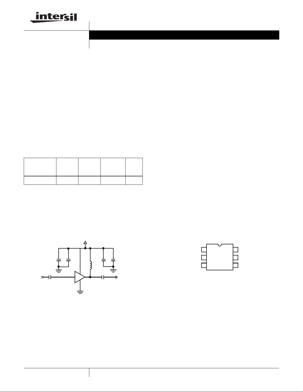
Typical Application Circuit Pinout
+3.3V
0.1µF
68pF 68pF
100pF
3
1, 2, 5
100pF
100nH
4
6
1
0.1µF
CAUTION: These devices are sensitive to electrostatic discharge; follow proper IC Handling Procedures.
1-888-INTERSIL or 1-888-468-3774
6 LD SC-70
GND
1
GND
2
3
IN
| Intersil (and design) is a registered trademark of Intersil Americas Inc.
All other trademarks mentioned are the property of their respective owners.
Copyright © Intersil Americas Inc. 2006. All Rights Reserved.
6
OUT
5
GND
4
VSP
Page 2
ISL55005
Absolute Maximum Ratings (T
Supply Voltage from VSP to GND . . . . . . . . . . . . . . . . . . . . . . . . 6V
Input Voltage . . . . . . . . . . . . . . . . . . . . . . . V
Power Dissipation . . . . . . . . . . . .See Packging Information Section
Ambient Operating Temperature . . . . . . . . . . . . . . . .-40°C to +85°C
= 25°C)
A
+ +0.3V to GND -0.3V
S
Storage Temperature. . . . . . . . . . . . . . . . . . . . . . . .-65°C to +125°C
Operating Junction Temperature . . . . . . . . . . . . . . . . . . . . . .+125°C
ESD Rating
Human Body Model (Per MIL-STD-883 Method 3015.7). . .3000V
Machine Model (Per EIAJ ED-4701 Method C-111). . . . . . . .300V
CAUTION: Stresses above those listed in “Absolute Maximum Ratings” may cause permanent damage to the device. This is a stress only rating and operation of the
device at these or any other conditions above those indicated in the operational sections of this specification is not implied.
IMPORTANT NOTE: All parameters having Min/Max specifications are guaranteed. Typ values are for information purposes only. Unless otherwise noted, all test s are
at the specified temperature and are pulsed tests, therefore: T
= TC = T
J
A
Electrical Specifications VSP = +3.3V, Zrsc = Zload = 50Ω, TA = 25°C, unless otherwise specified.
PARAMETER DESCRIPTION CONDITIONS MIN TYP MAX UNIT
Gt Small Signal Gain 1.0GHz 16.2 17.2 18.2 dB
1.5GHz 16.0 17.0 18.0 dB
2.0GHz 15.6 16.6 17.6 dB
P1dB Output Power at 1dB Compression 1.0GHz 5.5 7.5 9.5 dBm
2.0GHz 4.9 6.4 7.9 dBm
OIP3 Output Third Order Intercept Point 1.0GHz 18.0 dBm
2.0GHz 17.3 dBm
BW 3dB Bandwidth 3dB below Gain @ 500MHz 3.0 GHz
IRL Input Return Loss 1.0GHz Zrsc = 75Ω, Zload = 50Ω 14.5 dB
ORL Output Return Loss 1.0GHz Zrsc = 75Ω, Zload = 50Ω 17.6 dB
RISOL Reverse Isolation 2.0GHz 21.8 dB
NF Noise Figure 2.0GHz 3.6 dB
ID Device Operating Current 17.5 20.6 23.5 mA
Device Test Setup
Agilent _8753ES
VNA
CONNECTORLESS
PLATFORM
DC BLOCK DUT BIAS TEE
PICOSECOND LABS
MODEL 5508-110
50Ω 50Ω
PIN 3 PIN 6
INPUT
REFERENCE
PLANE
3.3V
OUTPUT
REFERENCE
PLANE
PICOSECOND LABS
MODEL 5542
I
1
3.3V
POWER
SUPPLY
50Ω50Ω
I
2
I
DEVICE
2
FN6199.0
May 22, 2006
Page 3

ISL55005
Typical Performance Curves Z
20
16
12
8
IRL (dB)
4
0
0.5 1.0 1.5 2.0 2.5 3.0
Frequency (GHz)
= 75Ω, Z
src
load
= 50Ω
20
16
12
8
ORL (dB)
4
0
0.5 1.0 1.5 2.0 2.5 3.0
Frequency (GHz)
FIGURE 1. INPUT RETURN LOSS vs FREQUENCY FIGURE 2. OUTPUT RETURN LOSS vs FREQUENCY
Typical Performance Curves 50Ω environment
(dB)
S
21
18.0
17.2
16.4
15.6
14.8
(dB)
S
11
-8.0
-8.6
-9.2
-9.8
-10.4
14.0
0.5 1.0 1.5 2.0 2.5 3.0
FREQUENCY (GHz)
-11.0
0.5 1.0 1.5 2.0 2.5 3.0
FREQUENCY (GHz)
FIGURE 3. |S21| vs FREQUENCY FIGURE 4. |S11| vs FREQUENCY
-21.0
-21.4
-21.8
(dB)
-22.2
12
S
-22.6
-23.0
0.5 1.0 1.5 2.0 2.5 3.0
FREQUENCY (GHz)
-9.0
-9.8
-10.6
(dB)
-11.4
22
S
-12.2
-13.0
0.5 1.0 1.5 2.0 2.5 3.0
FREQUENCY (GHz)
FIGURE 5. |S12| vs FREQUENCY FIGURE 6. |S22| vs FREQUENCY
3
FN6199.0
May 22, 2006
Page 4

ISL55005
Typical Performance Curves 50Ω environment (Continued)
21
8.0
20
19
(dB m )
18
3
OIP
17
16
0.5 1.0 1.5 2.0 2.5 3.0
FREQUENCY (GHz)
7.6
7.2
6.8
(dBm)
6.4
1dBm Output Compression Point
6.0
0.5 1.0 1.5 2.0 2.5 3.0
FREQUENCY (GHz)
FIGURE 7. OIP3 vs FREQUENCY FIGURE 8. P1dB vs FREQUENCY
5
4
3
2
Noise Figure (dB)
1
0
0.5 1.0 1.5 2.0 2.5 3.0
FREQUENCY (GHz)
FIGURE 9. NOISE FIGURE vs FREQUENCY
9
.
1.0
0.9
1.0
3 GHz
1.0
2
.
0
4
.
0
6
.
0
6
.
0
4
.
0
2
.
0
1.2
2
.
0
0.5 GHz
4
.
0
6
.
0
1.0
6
.
0
4
.
0
2
.
0
2
.
1
4
.
1
6
.
1
8
.
1
0
.
2
0
.
3
8
.
0
0
.
1
0
.
1
8
.
0
1.4
1.6
1.8
2.0
3.0
4.0
0.5 GHz
1.0
8
.
0
2.2
0
.
1
S11
0
.
1
8
.
0
0
.
2
8
.
1
6
.
1
4
.
1
2
.
1
0
.
4
0
.
5
0
.
6
0
.
7
0
.
8
0
.
9
0
1
0
2
0
5.0
5
10
50
20
0
5
2
0
0
1
0
.
9
0
.
8
0
.
7
0
.
6
0
.
5
0
.
4
0
.
3
0
8
.
0
7
.
0
6
.
0
5
.
0
4
.
0
3
.
0
2
.
0
1
.
0
0
0.1
1
.
0
0.3
0.4
0.5
0.6
0.7
0.2
0.8
S22
3 GHz
2.2
2
.
0
3
.
0
4
.
0
5
.
0
6
.
0
7
.
0
8
.
0
9
.
0
RF Café 2002
FIGURE 10. S11 AND S22 vs FREQUENCY
4
FN6199.0
May 22, 2006
Page 5

Packaging Information
JEDEC JESD51-7 HIGH EFFECTIVE THERMAL
JEDEC JESD51-7 HIGH EFFECTIVE THERMAL
CONDUCTIVITY TEST BOARD
CONDUCTIVITY TEST BOARD
0.3
0.25
0.2
176mW
0.15
0.1
POWER DISSIPATION (W)
POWER DISSIPATION (W)
0.05
0
0
0
0
FIGURE 11. PACKAGE POWER DISSIP A TION vs AMBIENT
TEMPERATURE
S
C
θ
7
J
0
A
=
-
6
5
6
7
°
C
/
W
AMBIENT TEMPERATURE (°C)
AMBIENT TEMPERATURE (°C)
1507525 10050 12585
1507525 10050 12585
ISL55005
5
FN6199.0
May 22, 2006
Page 6

ISL55005
Small Outline Transistor Plastic Packages (SC70-6)
C
L
A2
A
SEATING
PLANE
0.20 (0.008)
C
L
b
123
e1
D
C
L
WITH
PLATING
4X θ1
C
4X θ1
M
e
456
0.10 (0.004) C
c
BASE METAL
L1
C
VIEW C
P6.049
6 LEAD SMALL OUTLINE TRANSISTOR PLASTIC PACKAGE
INCHES MILLIMETERS
SYMBOL
NOTESMIN MAX MIN MAX
A 0.031 0.043 0.80 1.10 -
C
L
E
E1
A1 0.000 0.004 0.00 0.10 A2 0.031 0.039 0.00 1.00 -
b 0.006 0.012 0.15 0.30 -
b1 0.006 0.010 0.15 0.25
c 0.003 0.009 0.08 0.22 6
C
c1 0.003 0.009 0.08 0.20 6
D 0.073 0.085 1.85 2.15 3
E 0.071 0.094 1.80 2.40 -
E1 0.045 0.053 1.15 1.35 3
e 0.0256 Ref 0.65 Ref -
e1 0.0512 Ref 1.30 Ref -
A1
SEATING
PLANE
-C-
L 0.010 0.018 0.26 0.46 4
L1 0.017 Ref. 0.420 Ref.
L2 0.006 BSC 0.15 BSC
b
b1
c1
N6 65
R 0.004 - 0.10 -
R1 0.004 0.010 0.15 0.25
o
α
0
o
8
o
0
o
8
-
Rev. 2 9/03
NOTES:
1. Dimensioning and tolerance per ASME Y14.5M-1994.
2. Package conforms to EIAJ SC70 and JEDEC MO203AB.
R1
R
GAUGE PLANE
L
α
L2
3. Dimensions D and E1 are exclusive of mold flash, protrusions,
or gate burrs.
4. Footlength L measured at reference to gauge plane.
5. “N” is the number of terminal positions.
6. These Dimensions apply to the flat section of the lead between
0.08mm and 0.15mm from the lead tip.
7. Controlling dimension: MILLIMETER. Converted inch dimensions are for reference only
VIEW C
All Intersil U.S. products are manufactured, assembled and tested utilizing ISO9000 quality systems.
Intersil Corporation’s quality certifications can be viewed at www.intersil.com/design/quality
Intersil products are sold by description only. Intersil Corporation reserves the right to make changes in circuit design, software and/or specifications at any time without
notice. Accordingly, the reader is cautioned to verify that data sheets are current before placing orders. Information furnished by Intersil is believed to be accurate and
reliable. However, no responsibility is assumed by Intersil or its subsidiaries for its use; nor for any infringements of patents or other rights of third parties which may result
from its use. No license is granted by implicat ion or oth erwise u nde r any p a tent or p at ent r ights of Intersil or its subsidiaries.
For information regarding Intersil Corporation and its products, see www.intersil.com
6
FN6199.0
May 22, 2006
 Loading...