

Page 1
®
ISL54207EVAL1Z Evaluation Board User’s
Manual
AN1358.0Application Note June 23, 2008
Description
The ISL54207EVAL1Z evaluation board is designed to
provide a quick and easy method for evaluating the
ISL54207 USB/CVBS/Audio IC.
The ISL54207 device is an unique IC. T o use this evaluation
board properly, requires a thorough knowledge of the
operation of the IC. Refer to the ISL54207 datasheet for an
understanding of the functions and features of the device.
Studying the device’s truth table along with its “Pinout”
diagram on page 2 of the ISL54207 datasheet, is the best
way to get a quick understanding of how the part works.
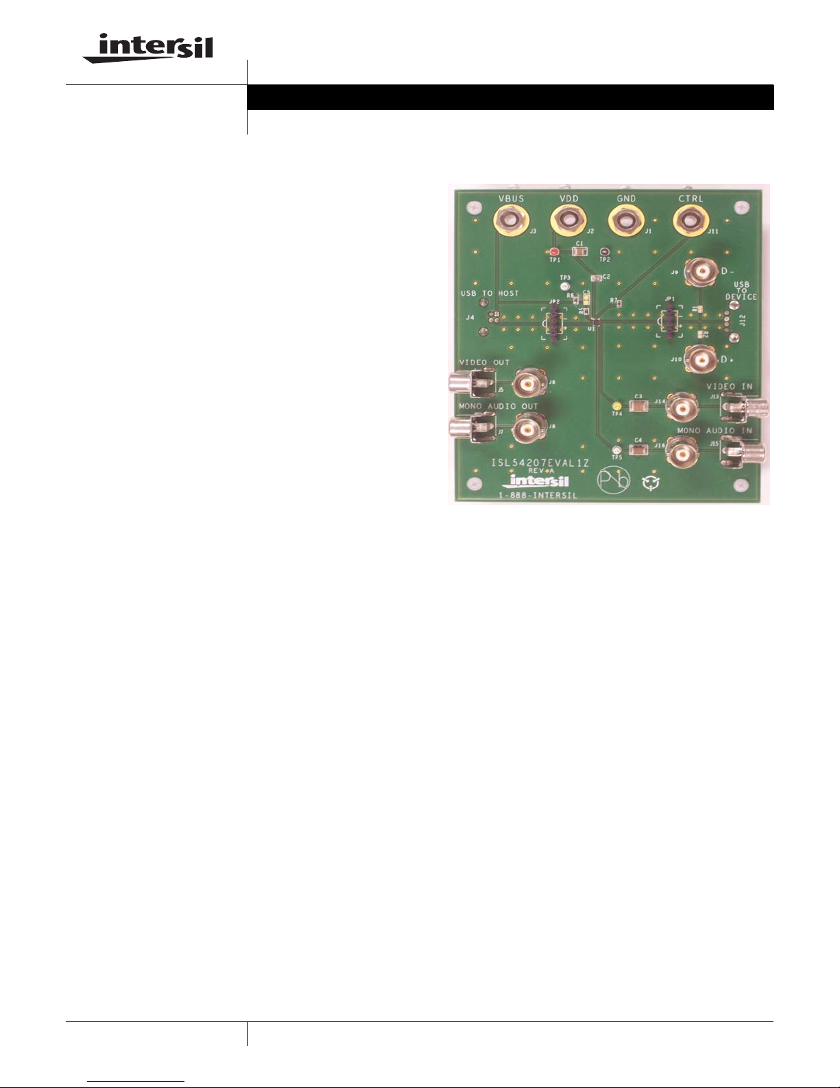
A picture of the main evaluation board is shown in Figure 1.
The ISL54207 µTQFN IC is soldered onto the evaluation
board. It is located in the center of the board and is
designated as U1.
The ISL54207 IC is a dual SPDT analog switch that was
designed to multiplex between mono audio/video (A/V)
signals or USB differential signals of a portable media player
such as digital cameras, camcorders, MP3 players and
cellphones.
The part has two modes of operation: Audio/Video mode and
USB mode. The evaluation board contains standard RCA,
BNC, and USB connectors to allow the user to easily
interface with the IC to evaluate its functions, features, and
performance in these two modes of operation.
For example, when the board is properly powered, the
video/mono audio outputs of a video MP3 player can be
connected at RCA connectors J13 (VIDEO IN) and J15
(MONO AUDIO IN) and the USB output of the player can be
connected at the USB connector J12 (USB TO DEVICE) on
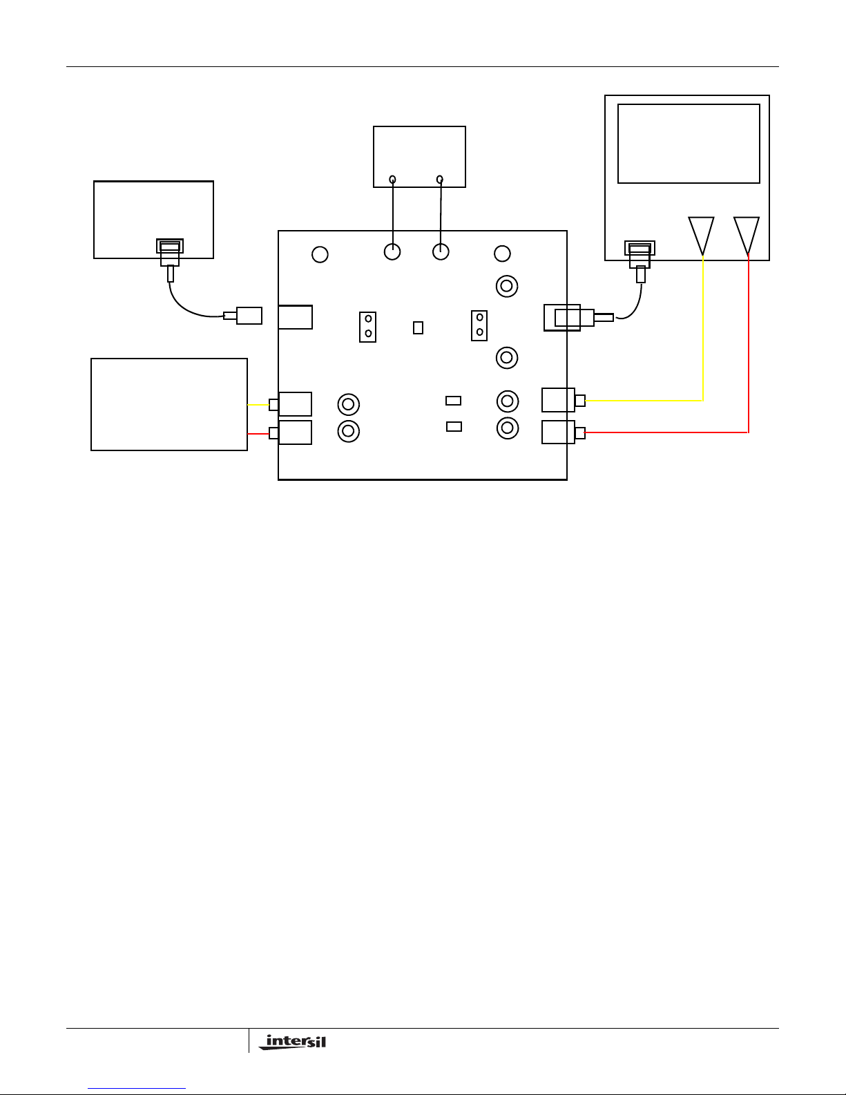
the board. See Figure 2 on page 4. A TV can be connected
at RCA jacks J5 (VIDEO OUT) and J7 (MONO AUDIO OUT)
to play the video on the TV. You can then turn-off the video,
disconnected the TV, and attach a USB cable from a
computer to USB connector J4 (USB TO HOST) to load
digital video tracks into the player.
This application note will guide the user through the process
of configuring and using the evaluation board to evaluate the
ISL54207 device in both the Audio/Video mode and the USB
mode.
Key Features
• Standard USB Connectors
• RCA Audio/Video Input Jacks and BNC Connectors
• Convenient Test Points and Connections for Test
Equipment
Picture of Evaluation Board (Top View)
FIGURE 1. ISL54207EVAL1Z EVALUATION BOARD
Board Architecture/Layout
Basic Layout of Evaluation Board
The basic layout of the main board is as follows: Refer to
Figure 1.
Power (J2), GND (J1), logic VBUS (J3) and logic CTRL (J11)
banana jack connections are at the top of the board.
Audio/Video Source RCA inputs are at the lower right side of
the board (J13 and J15). Audio/Video RCA outputs are at
the lower left side of the board (J5 and J7).
A standard “B” type USB connection to an upstream host
controller (Computer) is made at connector J4, located on
left underside of the board. A standard “A” type USB
connection to a downstream USB device is made at
connector J12, located on right underside of the board.
Located in the center of the board is the ISL54207 IC (U1).
The evaluation board has a pin 1 dot, to show how the IC
should be oriented onto the evaluation board. The IC pin 1
indicator dot needs to be aligned with the evaluation board
pin 1 dot indicator.
Note: The connectors J5 (VIDEO OUT) and J7 (MONO
AUDIO OUT) are connected in parallel to J4 (USB TO
HOST). When driving the USB input, the A/V output should
be in a high impedance state (and vice versa).
1
CAUTION: These devices are sensitive to electrostatic discharge; follow proper IC Handling Procedures.
1-888-INTERSIL or 1-888-468-3774
| Intersil (and design) is a registered trademark of Intersil Americas Inc.
All other trademarks mentioned are the property of their respective owners.
Copyright Intersil Americas Inc. 2008. All Rights Reserved
Page 2

Application Note 1358
Power Supply
The DC power supply connected at banana jacks J2 (VDD)
and J1 (GND) provides power to the evaluation board. The
IC requires a +2.7V to +3.6VDC power supply for proper
operation. The power supply should be capable of delivering
100
µA of current.
Logic Control
The state of the ISL54207 device is determined by the
voltage at the VBUS pin and the CTRL pin. Access to the
CTRL pin is through the banana jack J11 (CTRL) and access
to the VBUS pin is through the USB J4 connector or the
banana jack J3 (VBUS).
The CTRL logic control pin is 1.8V logic compatible which
allows for control via a standard
mcontroller. In a typical
application, the VBUS logic control pin will be driven by the
VBUS
(4.4V to 5.25V) of the USB Host controller. An internal
4M
W pull-down resistor on the IC will drive the logic low
when the pin is floating.
V
= Logic “0” (Low) when VBUS ≤ VDD + 0.2V or
BUS
Floating.
VBUS = Logic “1” (High) when VBUS
CTRL = Logic “0” (Low) when
CTRL = Logic “1” (High) when
If V
is floating (no USB host controller connected at the
BUS
≥ V
+ 0.8V
≤ 0.5V or floating.
≥ 1.4V
DD
J4 connector) and CTRL is HIGH (J11 connected to J2) the
part will be in the Audio/Video mode. The audio/video
switches will be ON and the USB switches will be OFF.
There will be a low impedance path from VIDEO IN to
VIDEO OUT and from MONO AUDIO IN to MONO AUDIO
OUT.
If VBUS is driven HIGH and CTRL = X (don’t care) the part
will be in the USB mode. The USB switches will be ON and
the audio/video switches will be OFF. There will be a low
impedance path from USB TO DEVICE to USB TO HOST.
If VBUS = LOW and CTRL = LOW the part will be in the Low
Power mode. In Low Power mode all switches are OPEN
and the IC will draw around 1nA of current.
When the USB connector at J4 is not connected to a USB
port on a computer, the 4MΩ pull-down will pull the VBUS
pin LOW putting the ISL54207 in the Audio/Video mode or
Low Power mode depending on the condition of the CTRL
pin. When a connection to a computer USB host is present
on J4, the voltage at the VBUS pin will be driven to 5V and
the part will automatically go into the USB mode.
Audio/Video Inputs
The evaluation board has two audio/video inputs labeled
VIDEO IN (J13) and MONO AUDIO IN (J15). Each of these
inputs have a BNC connector (J14 and J16 respectively)
wired in parallel with the RCA connector. Y ou can connect an
audio/video source or generator at either the BNC connector
or the RCA connector.
In a typical application the composite video output (NTSC or
PAL) and the mono audio output of the video source, (i.e.
TV , video MP3 Player , digital camera, cellphone, etc.), would
be connected to the RCA jacks J13 for video and J15 for
mono audio on the evaluation board.
Over a signal range of ±1V (0.707V
have an extremely low r
resistance variation (0.03Ω).
ON
) these switches
RMS
They can pass ground referenced audio/video signals up to
0.707V
3V
P-P
with very low distortion and degradation. A
RMS
signal is acceptable but performance will degrade.
The audio/video channels are AC coupled with 100µF
capacitors (C
and C4). These capacitors remove any DC
3
voltage from the audio/video signals and reference them to
ground of the device. If the audio/video source being
connected to the evaluation board already has internal
AC-coupling capacitors at the output of its drivers then the
capacitors on the evaluation board should be shorted out
(replaced with 0Ω resistors). This will prevent further
attenuation of the low frequency content of the audio signal
due to the increase of the high-pass corner frequency
resulting from the evaluation board capacitor in series with
the audio/video source capacitor.
Note: When in USB mode the audio/video source needs to
be in a high impedance state so it will not interfere with the
USB signal. Since the audio/video source inputs are
AC-coupled on the evaluation board, simply turning the
audio/video source OFF will isolate it from interfering with
the USB signal.
Audio/Video Outputs
The evaluation board has RCA type connectors labeled J5
and J7 for A/V output connections. For video playback, a TV
monitor should be connected at these connectors using a
standard A/V cable. The video input port of the TV should be
connected to VIDEO OUT (J5) and the audio input port of
the TV should be connected to MONO AUDIO OUT (J7).
The BNC connector J6 is in parallel with J5 and the D- line of
the J4 (USB TO HOST) connector. The BNC connector J8 is
in parallel with J7 and the D+ line of the J4 (USB TO HOST)
connector. These BNC connectors can be used to connect
resistive loads and/or test equipment to evaluate the
performance of the IC.
Note: When in USB mode, devices on the audio/video
outputs need to be in a high impedance state so it will not
interfere with the USB signal, since the USB and A/V
connections on the output/upstream side are all wired in
parallel.
USB Connections
A “B” type USB receptacle labeled “USB TO HOST” (J4) is
located on the left underside of the board. This receptacle
should be connected, using a standard USB cable, to the
up-stream USB host controller which is usually a PC
computer or hub. When this connection is made the
2
AN1358.0
June 23, 2008
Page 3
Application Note 1358
ISL54207 device will sense the VBUS voltage from the
computer, and will go into USB mode. High Speed USB
signals can be passed between J4 and J12.
An “A” type USB receptacle labeled USB TO DEVICE (J12)
is located on the right underside of the board. The USB
device can be plugged directly into this receptacle or through
a standard USB cable.
In USB mode the USB host controller and USB device will
be connected through the internal USB switches of the IC.
The USB switches are bi-directional which allow the host
(computer) and downstream USB device to both send and
receive data.
JP1 and JP2 permit the connection of differential probes for
monitoring of the USB signals. JP1 is used for monitoring on
the device side. JP2 is used for monitoring on the host side.
In addition, BNC connectors J9 (D-) and J10 (D+) can be
connected in parallel to J12 for monitoring the USB signals
on the device side using an oscilloscope. Normally, J9 and
J10 are not connected to the USB signal path. If the user
requires BNC connections to the USB signals on the device
side, then R
populated with 0Ω
and R2 on the evaluation board can be
1
resistors. R
and R2 are located between
1
the J9 and J10 BNC connectors.
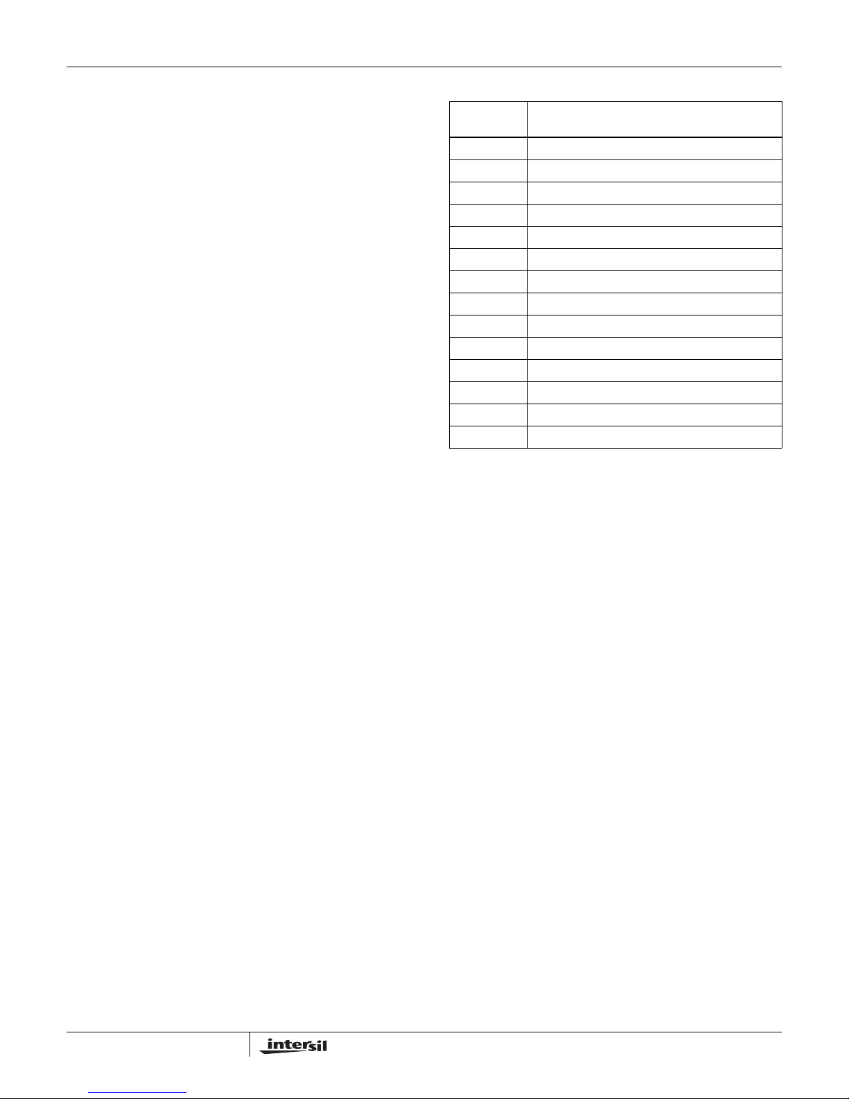
Board Component Definitions
DESIGNATOR DESCRIPTION
U1 ISL54207IRUZ IC
J1 Ground Connection
J2 V
J3 VBUS Logic Input
J4 “B” type USB Receptacle
J5, J6 VIDEO OUT Outputs
J7, J8 MONO AUDIO OUT Outputs
J9 USB (D-) BNC Connector
J10 USB (D+) BNC Connector
J11 CTRL Logic Input
J12 “A” type USB Receptacle
J13, J14 VIDEO IN Inputs
J15, J16 MONO AUDIO IN Inputs
JP1, JP2 D-/D+ Differential Probe Connection
Positive Connection
DD
Note: Before connecting the USB host controller at
connector J4, the A/V connections must be disconnected (or
set to high impedance) from the VIDEO OUT and MONO
AUDIO OUT connectors (J5-J8). This will prevent the
audio/video load from interfering with USB signal
transmission.
Application
The main purpose of the ISL54207 device is to allow the use
of a common USB and Audio/Video Connector in Personal
Media Players and other portable battery-powered
equipment. Either a TV monitor will be in the common
connector to play video or a USB cable from a computer will
be in the common connector to transmit digital data, such as
music videos or MP3 songs into the memory of the Media
Player.
3
AN1358.0
June 23, 2008
Page 4
Application Note 1358
COMPUTER
USB PORT
TV MONITOR
AV VIDEO
AV AUDIO
DC POWER
SUPPLY
+3.3V
+
VBUS
USB TO HOST
J4
VIDEO OUT
J5
J7
MONO AUDIO OUT
FIGURE 2. BASIC EVALUATION TEST SETUP BLOCK DIAGRAM
VDD
J3
JP2
ISL54207EVAL1Z EVALUATION BOARD
J2
J6
J8
GND
U1
-
J1
JP1
C3
C4
CTRL
J11
J9
J10
J14
J16
MONO AUDIO IN
USB
DEVICE
J12
VIDEO IN
J13
J15
TO
VIDEO MP3 PLAYER
VIDEO
DRIVER
USB PORT
COMPOSITE VIDEO
MONO AUDIO
AUDIO
DRIVER
Using The Board (Refer to Figure 2)
Lab Equipment
The equipment, external supplies and signal sources
needed to operate the board are listed below:
1. +3V to 5V DC Power Supply
2. Audio/Video Media Player with USB connector (video
MP3, digital camera, camcorder) or Audio/Video
Generator
3. TV Monitor or Audio/Video Analyzer/Oscilloscope
4. Two standard USB cables
5. Computer with USB port
Initial Board Setup Procedure
1. Attach the main evaluation board to the DC power supply
at J2 (V
negative terminal at J1. The supply should be capable of
delivering 3V to 5V and 100µ
voltage to 3.3V.
2. Connect the media player’s composite video source to
the J13 RCA connector or the J14 BNC connector and
the mono audio source to the J15 RCA connector or J16
BNC connector. Set the media player to output either
NTSC or PAL composite video signal.
3. Connect the USB port of the media player to the USB “A”
type receptacle, J12 (USB TO DEVICE).
) and J1 (GND). Positive terminal at J2 and
DD
A of current. Set the supply
Audio/Video Mode Operation
1. Connect the TV monitor AV video input at J5 (VIDEO
OUT) and the AV audio input at J7 (MONO AUDIO OUT).
No USB cable should be connected at the J4 (USB TO
HOST) connector.
2. Set the TV to receive the video signal through its AV input
and set to the appropriate channel.
3. Connect J11 (CTRL) to J2 (VDD). You will now be in
Audio/Video mode (3Ω NC switches are ON).
4. Turn the audio/video media player ON. You should hear
and see the video on the TV screen.
5. Y ou can observe the audio/video signals at the output of
the IC on an oscilloscope or audio/video analyzer by
using the J6 and J8 BNC connectors or appropriate test
points.
USB Mode Operation
1. Turn OFF the audio/video from the media player.
2. Disconnect the TV monitor from J5 and J7 RCA
connectors.
3. Connect a USB cable from host (PC computer) to the
USB “B” type receptacle, J4 (USB TO HOST). You will
now be in USB mode (5Ω NO switches are ON).
4. You should now be able to send and receive data
between the host and USB device.
5. Remove the 0Ω resistors R
signal quality performance (i.e. eye diagram, etc.) of the
high speed USB signal. Removal of these resistors
and R4 when evaluating the
3
4
AN1358.0
June 23, 2008
Page 5
Application Note 1358
disconnects the RCA connectors (J5 and J7) and the
BNC connectors (J6 and J8) from the USB differential
lines. These components when connected will degrade
the USB signal. These components will not be there in an
actual application. Note: R
and R4 are located on the
3
underside of the board.
If you disconnect the USB cable from J4 the IC will return to
Audio mode. You can now plug the TV monitor into J5 and
J7, turn the audio/video of the player ON to once again play
the music video or movie.
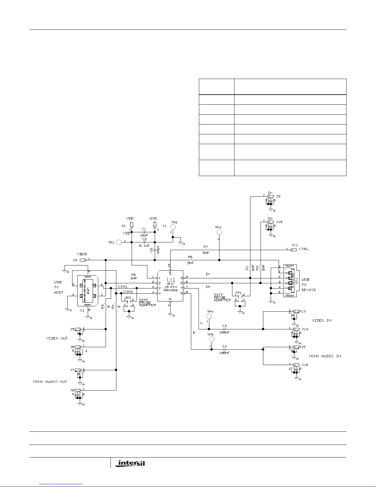
Board Schematic
USB
TO
HOST
VIDEO OUT
MONO A UDIO OUT
VDD
J2
1
VDD
1
TP1
VBUS
1
J3
A
MOUNT
897-30-004-90-000
2
3
3
4
4
A
J4
J5
432
A
J6
5
4
3
A
J7
432
A
J8
5
3
4
A
2
USB
1
1
MOUNT
65
A
1
1
2
1
1
2
0
R3
DNP
COM1
COM2
JP2
1
3
0
R4
C1
10UF
GND
C2
TP2
J1
1
1
0.1UF
C5
OPEN
10
R5
2
4
A
1
2
3
4
DIFF ADAPTER
PROBE
ADAPTER
1
2
3
46
10
U1
QFN
10 PIN
PACKAGE
5
5
Tes t Points
The evaluation board has various test points for ease of
connecting probes to make measurements. The test points
available are described in Table 1.
TABLE 1. TEST POINT DESCRIPTIONS
DESIGNATOR DESCRIPTION
TP1 V
TP2 Ground Test Point
TP3 V
TP4 VIDEO IN Test Point
TP5 MONO AUDIO IN Test Point
JP1 D-/D+ Differential Probe Connection - USB Device
JP2 D-/D+ Differential Probe Connection - HOST Side
TP3
A
R6
DNP
9
9
8
8
7
7
6
A
R
1
R7
DNP
D-
D+
DIFF
PROBE
TP4
1
L
TP5
C3
100UF
1
C4
100UF
test point
DD
Test Point
BUS
Side of Switch
of Switch
R2
R1
DNP
JP1
2
1
4
3
A
1
1
DNP
D-
J9
5
2
3
4
A
D+
J10
5
2
3
4
A
J11
1
CTRL
MOUNT
5
1
1
USB TYPE A
2
2
J12
USB
3
3
4
6
A
MOUNT
TO
4
DEVICE
1
J13
432
VIDEO IN
A
1
J14
5
2
3
4
A
1
J15
432
MONO AUDIO IN
A
1
J16
5
2
4
3
A
IN
Intersil Corporation reserves the right to make changes in circuit design, software and/or specifications at any time without notice. Accordingly, the reader is cautioned to
verify that the Application Note or Technical Brief is current before proceeding.
For information regarding Intersil Corporation and its products, see www.intersil.com
5
AN1358.0
June 23, 2008
 Loading...