

Page 1
®
HIN202E, HIN206E, HIN207E, HIN208E,
HIN211E, HIN213E, HIN232E
Data Sheet August 2002
+/-15kV, ESD-Protected, +5V Powered,
RS-232 Transmitters/Receivers
The HIN202E - HIN232E family of RS-232
transmitters/receivers interface circuits meet all ElA highspeed RS-232E and V.28 specifications, and are particularly
suited for those applications where ±12V is not available. A
redesigned transmitter circuit improves data rate and slew
rate, which makes this suitable for ISDN and high speed
modems. The transmitter outputs and receiver inputs are
protected to ±15kV ESD (Electrostatic Discharge). They
require a single +5V power supply and feature onboard
charge pump voltage converters which generate +10V and
-10V supplies from the 5V supply. The family of devices
offers a wide variety of high-speed RS-232
transmitter/receiver combinations to accommodate various
applications (see Selection Table).
The HIN206E, HIN211E and HIN213E feature a low power
shutdown mode to conserve energy in battery powered
applications. In addition, the HIN213E provides two active
receivers in shutdown mode allowing for easy “wakeup”
capability.
The drivers feature true TTL/CMOS input compatibility, slew
rate-limited output, and 300Ω power-off source impedance.
The receivers can handle up to ±30V input, and have a 3kΩ
to 7kΩ input impedance. The receivers also feature
hysteresis to greatly improve noise rejection.
FN4315.10
Features
• High Speed ISDN Compatible . . . . . . . . . . . . . 230kbits/s
• ESD Protection for RS-232 I/O Pins to ±15kV (IEC1000)
• Meets All RS-232E and V.28 Specifications
• Requires Only 0.1µF or Greater External Capacitors
• Two Receivers Active in Shutdown Mode (HIN213E)
• Requires Only Single +5V Power Supply
• Onboard Voltage Doubler/Inverter
• Low Power Consumption (Typ) . . . . . . . . . . . . . . . . . 5mA
• Low Power Shutdown Function (Typ) . . . . . . . . . . . . .1µA
• Three-State TTL/CMOS Receiver Outputs
• Multiple Drivers
- ±10V Output Swing for +5V Input
-300Ω Power-Off Source Impedance
- Output Current Limiting
- TTL/CMOS Compatible
• Multiple Receivers
- ±30V Input Voltage Range
-3kΩ to 7kΩ Input Impedance
- 0.5V Hysteresis to Improve Noise Rejection
Applications
• Any System Requiring High-Speed RS-232
Communications Port
- Computer - Portable, Mainframe, Laptop
- Peripheral - Printers and Terminals
- Instrumentation, UPS
- Modems, ISDN Terminal Adaptors
Selection Table
NUMBER OF
NUMBER OF
PART
NUMBER
HIN202E +5V 2 2 4 Capacitors NO/NO 0
HIN206E +5V 4 3 4 Capacitors YES/YES 0
HIN207E +5V 5 3 4 Capacitors NO/NO 0
HIN208E +5V 4 4 4 Capacitors NO/NO 0
HIN211E +5V 4 5 4 Capacitors YES/YES 0
HIN213E +5V 4 5 4 Capacitors YES/YES 2
HIN232E +5V 2 2 4 Capacitors NO/NO 0
POWER SUPPLY
VOLTAGE
RS-232
DRIVERS
NUMBER OF
RS-232
RECEIVERS
0.1µF
EXTERNAL
CAPACITORS
LOW POWER
SHUTDOWN/TTL
THREE-STATE
NUMBER OF
RECEIVERS
ACTIVE IN
SHUTDOWN
1
CAUTION: These devices are sensitive to electrostatic discharge; follow proper IC Handling Procedures.
1-888-INTERSIL or 321-724-7143
| Intersil (and design) is a registered trademark of Intersil Americas Inc.
Copyright © Intersil Americas Inc. 2002. All Rights Reserved
Page 2

HIN202E, HIN206E, HIN207E, HIN208E, HIN211E, HIN213E, HIN232E
Ordering Information
TEMP.
PART NO.
HIN202ECB 0 to 70 16 Ld SOIC (W) M16.3
HIN202ECBN 0 to 70 16 Ld SOIC (N) M16.15
HIN202ECBN-T 0 to 70 Tape and Reel
HIN202ECP 0 to 70 16 Ld PDIP E16.3
HIN202EIB -40 to 85 16 Ld SOIC (W) M16.3
HIN202EIB-T -40 to 85 Tape and Reel
HIN202EIBN -40 to 85 16 Ld SOIC (N) M16.15
HIN202EIBN-T -40 to 85 Tape and Reel
HIN206ECB 0 to 70 24 Ld SOIC M24.3
HIN206ECB-T 0 to 70 Tape and Reel
HIN206ECP 0 to 70 24 Ld PDIP E24.3
HIN206EIA -40 to 85 24 Ld SSOP M24.209
HIN207ECA 0 to 70 24 Ld SSOP M24.209
HIN207ECA-T 0 to 70 Tape and Reel
HIN207ECB 0 to 70 24 Ld SOIC M24.3
HIN207ECB-T 0 to 70 Tape and Reel
HIN207EIB -40 to 85 24 Ld SOIC M24.3
HIN207EIB-T -40 to 85 Tape and Reel
HIN208ECA 0 to 70 24 Ld SSOP M24.209
HIN208ECA-T 0 to 70 Tape and Reel
HIN208ECB 0 to 70 24 Ld SOIC M24.3
HIN208ECB-T 0 to 70 Tape and Reel
HIN208EIA -40 to 85 24 Ld SSOP M24.209
HIN208EIB -40 to 85 24 Ld SOIC M24.3
RANGE (oC) PACKAGE PKG. NO.
Ordering Information (Continued)
TEMP.
o
PART NO.
HIN208EIP -40 to 85 24 Ld PDIP E24.3
HIN211ECA 0 to 70 28 Ld SSOP M28.209
HIN211ECA-T 0 to 70 Tape and Reel
HIN211ECB 0 to 70 28 Ld SOIC M28.3
HIN211EIA -40 to 85 28 Ld SSOP M28.209
HIN211EIB -40 to 85 28 Ld SOIC M28.3
HIN213ECA 0 to 70 28 Ld SSOP M28.209
HIN213ECA-T 0 to 70 Tape and Reel
HIN213EIA -40 to 85 28 Ld SSOP M28.209
HIN213EIA-T -40 to 85 Tape and Reel
HIN213EIB -40 to 85 28 Ld SOIC M28.3
HIN232ECA 0 to 70 16 Ld SSOP M16.209
HIN232ECA-T 0 to 70 Tape and Reel
HIN232ECB 0 to 70 16 Ld SOIC (W) M16.3
HIN232ECBN 0 to 70 16 Ld SOIC (N) M16.15
HIN232ECP 0 to 70 16 Ld PDIP E16.3
RANGE (
C) PACKAGE PKG. NO.
2
Page 3

Pinouts
HIN202E, HIN206E, HIN207E, HIN208E, HIN211E, HIN213E, HIN232E
HIN202E (PDIP, SOIC)
TOP VIEW
HIN206E (PDIP, SOIC, SSOP)
TOP VIEW
R1
R2
0.1µF
0.1µF
T1
T2
OUT
OUT
24
T4
OUT
23
R2
IN
22
R2
OUT
21
SD
20
EN
19
T4
IN
18
T3
IN
17
R3
OUT
16
R3
IN
15
V-
14
C2-
13
C2+
T2
C1+
C1-
C2+
C2-
OUT
R2
V+
V-
1
1
2
3
4
5
6
7
8
IN
16
V
CC
15
GND
14
T1
OUT
13
R1
IN
12
R1
OUT
11
T1
IN
10
T2
IN
9
R2
OUT
T3
T1
T2
R1
OUT
OUT
OUT
R1
OUT
T2
T1
GND
V
CC
C1+
V+
C1-
2
3
4
IN
5
6
IN
7
IN
8
9
10
11
12
+5V
+5V
16
1
C1+
+
3
C1-
4
C2+
+
5
C2-
+5V
400kΩ
11
IN
+5V
400kΩ
10
IN
V
CC
+5V TO 10V
VOLTAGE INVERTER
+10V TO -10V
VOLTAGE INVERTER
T1
T2
R1
R2
5kΩ
5kΩ
V+
V-
0.1µF
+
2
6
0.1µF
+
14
7
1312
89
T1
T2
R1
R2
OUT
OUT
IN
IN
0.1µF
0.1µF
R1
R2
10
C1+
+
12
C1-
13
+
14
T1
T2
T3
T4
OUT
OUT
7
IN
6
IN
18 1
IN
19 24
IN
VOLTAGE DOUBLER
C2+
VOLTAGE INVERTER
C2-
+5V
400kΩ
+5V
400kΩ
+5V
400kΩ
+5V
400kΩ
GND
15
R3
OUT
EN
20
9
V
CC
+5V TO 10V
+10V TO -10V
T1
T2
T3
T4
R1
R2
R3
5kΩ
5kΩ
5kΩ
V+
V-
0.1µF
+
11
15
0.1µF
+
2
3
T1
OUT
T2
OUT
T3
OUT
T4
R1
R2
R3
OUT
IN
IN
IN
45
2322
1617
21
SD
GND
8
3
Page 4
HIN202E, HIN206E, HIN207E, HIN208E, HIN211E, HIN213E, HIN232E
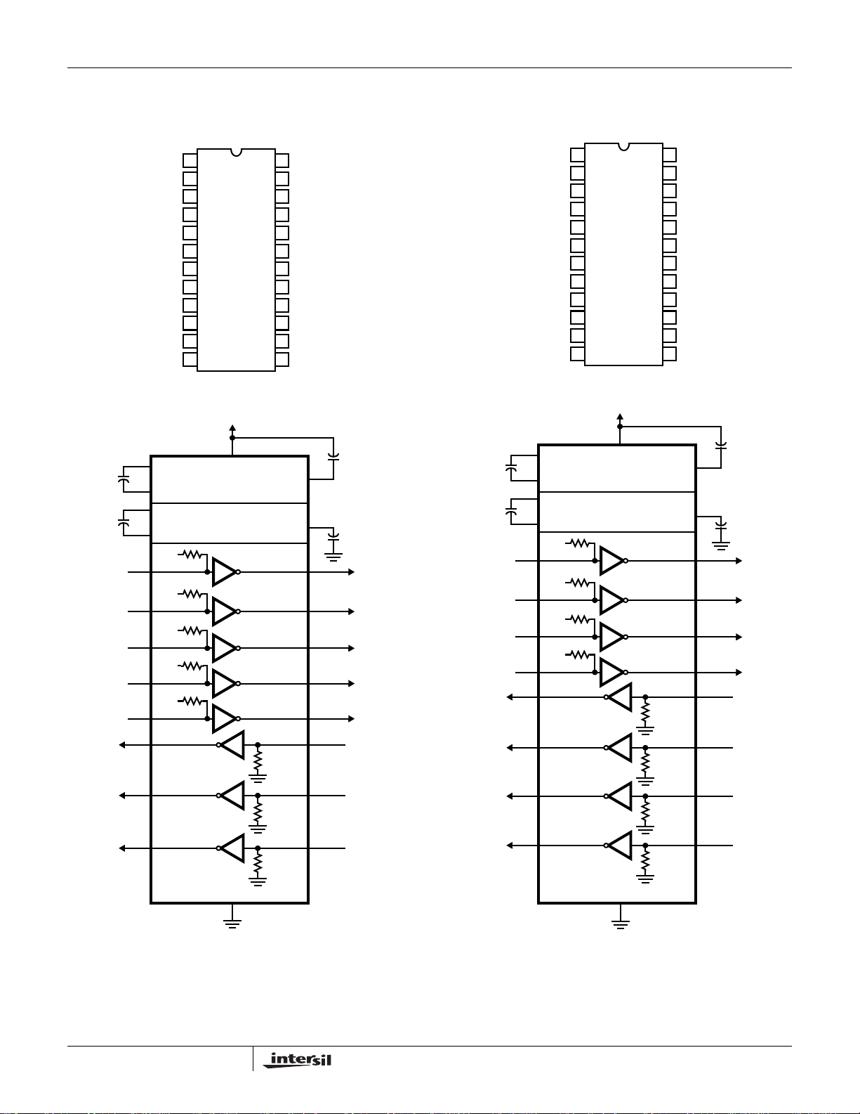
Pinouts (Continued)
HIN207E (SOIC, SSOP)
TOP VIEW
HIN208E (PDIP, SOIC, SSOP)
TOP VIEW
R1
R2
R3
0.1µF
0.1µF
T1
T2
T3
T4
T5
OUT
OUT
OUT
T3
1
OUT
T1
2
OUT
T2
3
OUT
R1
4
IN
R1
5
OUT
T2
6
IN
T1
7
IN
8
GND
V
9
CC
C1+
10
V+
11
C1-
12
TOP VIEW
+5V
10
C1+
+
12
C1-
13
+
14
IN
IN
18 1
IN
19 24
IN
21 20
IN
VOLTAGE DOUBLER
C2+
VOLTAGE INVERTER
C2-
+5V
400kΩ
7
+5V
400kΩ
6
+5V
400kΩ
+5V
400kΩ
+5V
400kΩ
9
V
CC
+5V TO 10V
+10V TO -10V
T1
T2
T3
T4
T5
R1
R2
R3
5kΩ
5kΩ
5kΩ
T2
1
24
T4
OUT
R2
23
IN
R2
22
OUT
T5
21
IN
T5
20
OUT
T4
19
IN
T3
18
IN
R3
17
OUT
R3
16
IN
V-
15
14
C2-
13
C2+
T1
R2
R1
OUT
OUT
R2
OUT
T1
OUT
R1
GND
V
CC
C1+
V+
C1-
2
3
IN
4
5
IN
6
7
IN
8
9
10
11
12
T3
24
OUT
R3
23
IN
R3
22
OUT
T4
21
IN
T4
20
OUT
T3
19
IN
T2
18
IN
R4
17
OUT
R4
16
IN
V-
15
C2-
14
C2+
13
+5V
V+
V-
10
0.1µF
+
11
15
0.1µF
+
2
3
45
2322
1617
T1
T2
T3
T4
T5
R1
R2
R3
OUT
OUT
OUT
OUT
OUT
IN
IN
IN
R1
R2
R3
R4
0.1µF
0.1µF
T1
T2
T3
T4
OUT
OUT
OUT
OUT
IN
IN
IN
IN
C1+
+
12
C1-
13
C2+
+
14
C2-
+5V
400kΩ
5
+5V
400kΩ
18
+5V
400kΩ
19 24
+5V
400kΩ
21 20
V
CC
+5V TO 10V
VOLTAGE DOUBLER
+10V TO -10V
VOLTAGE INVERTER
T1
T2
T3
T4
R1
R2
R3
R4
5kΩ
5kΩ
5kΩ
5kΩ
V+
V-
9
0.1µF
+
11
15
0.1µF
+
2
1
76
34
2322
1617
T1
T2
T3
T4
R1
R2
R3
R4
OUT
OUT
OUT
OUT
IN
IN
IN
IN
GND
GND
8
8
4
Page 5

HIN202E, HIN206E, HIN207E, HIN208E, HIN211E, HIN213E, HIN232E
Pinouts (Continued)
HIN211E (SOIC, SSOP)
T3
1
OUT
T1
2
OUT
3
T2
OUT
R2
4
IN
R2
5
OUT
T2
6
IN
T1
7
IN
R1
8
OUT
R1
9
IN
GND
10
V
11
CC
C1+
12
13
V+
14
C1-
TOP VIEW
HIN213E (SOIC, SSOP)
TOP VIEW
T4
T3
1
R2
R1
T1
T2
OUT
OUT
OUT
R2
OUT
T2
T1
OUT
R1
GND
V
CC
C1+
V+
C1-
2
3
4
IN
5
6
IN
7
IN
8
9
IN
10
11
12
13
14
28
T4
OUT
R3
27
IN
R3
26
OUT
SD
25
24
EN
R4
23
IN
R4
22
OUT
T4
21
IN
20
T3
IN
R5
19
OUT
R5
18
IN
V-
17
16
C2-
15
C2+
28
OUT
R3
27
IN
R3
26
OUT
SD
25
EN
24
23
R4
IN
R4
22
OUT
T4
21
IN
20
T3
IN
R5
19
OUT
R5
18
IN
V-
17
16
C2-
15
C2+
NOTE: R4 and R5 active in shutdown.
R1
R2
R3
R4
R5
0.1µF
0.1µF
T1
T2
T3
T4
OUT
OUT
OUT
OUT
OUT
EN
+5V
12
C1+
+
14
C1-
15
+
16
IN
IN
20 1
IN
21 28
IN
VOLTAGE DOUBLER
C2+
VOLTAGE INVERTER
C2-
+5V
400kΩ
7
+5V
400kΩ
6
+5V
400kΩ
+5V
400kΩ
11
V
CC
+5V TO 10V
+10V TO -10V
T1
T2
T3
T4
8
R1
R2
R3
R4
24
R5
GND
10
5kΩ
5kΩ
5kΩ
5kΩ
5kΩ
V+
V-
+5V
0.1µF
+
13
17
0.1µF
+
2
3
9
45
2726
2322
1819
25
T1
T2
T3
T4
R1
R2
R3
R4
R5
OUT
OUT
OUT
OUT
IN
IN
IN
IN
IN
SD
0.1µF
0.1µF
T1
T2
T3
T4
R1
R2
R3
R4
R5
12
C1+
+
14
C1-
15
+
16
7
IN
6
IN
20 1
IN
21 28
IN
EN
8
24
OUT
OUT
OUT
OUT
OUT
VOLTAGE DOUBLER
C2+
VOLTAGE INVERTER
C2-
+5V
400kΩ
+5V
400kΩ
+5V
400kΩ
+5V
400kΩ
11
V
CC
+5V TO 10V
+10V TO -10V
T1
T2
T3
T4
R1
R2
R3
R4
R5
5kΩ
5kΩ
5kΩ
5kΩ
5kΩ
V+
V-
0.1µF
+
13
17
0.1µF
+
2
3
9
45
2726
2322
1819
25
SD
T1
T2
T3
T4
R1
R2
R3
R4
R5
OUT
OUT
OUT
OUT
IN
IN
IN
IN
IN
GND
10
5
S
Page 6

HIN202E, HIN206E, HIN207E, HIN208E, HIN211E, HIN213E, HIN232E
Pinouts (Continued)
HIN232E (PDIP, SOIC, SSOP)
1
C1+
2
V+
3
C1-
4
C2+
5
C2-
6
V-
7
T2
OUT
8
R2
IN
TOP VIEW
+5V
16
1
C1+
+
16
V
CC
15
GND
14
T1
OUT
13
R1
IN
12
R1
OUT
11
T1
IN
10
T2
IN
9
R2
OUT
0.1µF
0.1µF
T1
T2
3
C1-
4
C2+
+
5
C2-
+5V
400kΩ
11
IN
+5V
400kΩ
10
IN
V
CC
+5V TO 10V
VOLTAGE INVERTER
+10V TO -10V
VOLTAGE INVERTER
T1
T2
V+
V-
0.1µF
+
2
6
0.1µF
+
14
7
T1
T2
OUT
OUT
R1
OUT
R1
R2
OUT
R2
GND
15
Pin Descriptions
PIN FUNCTION
V
CC
V+ Internally generated positive supply (+10V nominal).
V- Internally generated negative supply (-10V nominal).
GND Ground Lead. Connect to 0V.
C1+ External capacitor (+ terminal) is connected to this lead.
C1- External capacitor (- terminal) is connected to this lead.
C2+ External capacitor (+ terminal) is connected to this lead.
C2- External capacitor (- terminal) is connected to this lead.
T
IN
T
OUT
R
IN
R
OUT
EN
, EN Receiver Enable Input. With EN = 5V (HIN213E EN=0V), the receiver outputs are placed in a high impedance state.
SD, SD
NC No Connect. No connections are made to these leads.
Power Supply Input 5V ±10%, (5V ±5% HIN207E).
Transmitter Inputs. These leads accept TTL/CMOS levels. An internal 400kΩ pull-up resistor to V
CC
Transmitter Outputs. These are RS-232 levels (nominally ±10V).
Receiver Inputs. These inputs accept RS-232 input levels. An internal 5kΩ pull-down resistor to GND is connected to each input.
Receiver Outputs. These are TTL/CMOS levels.
Shutdown Input. With SD = 5V (HIN213E SD = 0V), the charge pump is disabled, the receiver outputs are in a high impedance
state (except R4 and R5 of HIN213E) and the transmitters are shut off.
1312
5kΩ
89
5kΩ
R1
R2
IN
IN
is connected to each lead.
6
Page 7

HIN202E, HIN206E, HIN207E, HIN208E, HIN211E, HIN213E, HIN232E
Absolute Maximum Ratings Thermal Information
VCC to Ground. . . . . . . . . . . . . . . . . . . . . . (GND -0.3V) < VCC < 6V
V+ to Ground . . . . . . . . . . . . . . . . . . . . . . . .(V
V- to Ground. . . . . . . . . . . . . . . . . . . . . . . .-12V < V- < (GND +0.3V)
-0.3V) < V+ < 12V
CC
Input Voltages
T
. . . . . . . . . . . . . . . . . . . . . . . . . . . . . -0.3V < VIN < (V+ +0.3V)
IN
R
. . . . . . . . . . . . . . . . . . . . . . . . . . . . . . . . . . . . . . . . . . . . ±30V
IN
Output Voltages
T
. . . . . . . . . . . . . . . . . . . .(V- -0.3V) < V
OUT
R
. . . . . . . . . . . . . . . . . (GND -0.3V) < V
OUT
TXOUT
RXOUT
< (V+ +0.3V)
< (V+ +0.3V)
Short Circuit Duration
T
. . . . . . . . . . . . . . . . . . . . . . . . . . . . . . . . . . . . . . Continuous
OUT
R
. . . . . . . . . . . . . . . . . . . . . . . . . . . . . . . . . . . . . . Continuous
OUT
ESD Classification . . . . . . . . . . . . . . . . . . . . See Specification Table
Thermal Resistance (Typical, Note 1)
16 Ld SOIC (N) Package . . . . . . . . . . . . . . . . . . . . . 110
16 Ld SOIC (W) Package. . . . . . . . . . . . . . . . . . . . . 100
16 Ld SSOP Package . . . . . . . . . . . . . . . . . . . . . . . 155
16 Ld PDIP Package . . . . . . . . . . . . . . . . . . . . . . . . 90
24 Ld SOIC Package . . . . . . . . . . . . . . . . . . . . . . . . 75
24 Ld SSOP Package . . . . . . . . . . . . . . . . . . . . . . . 135
24 Ld PDIP Package . . . . . . . . . . . . . . . . . . . . . . . . 75
28 Ld SOIC Package . . . . . . . . . . . . . . . . . . . . . . . . 70
28 Ld SSOP Package . . . . . . . . . . . . . . . . . . . . . . . 100
Maximum Junction Temperature (Plastic Package) . . . . . . . . 150
Maximum Storage Temperature Range. . . . . . . . . . -65
Maximum Lead Temperature (Soldering 10s) . . . . . . . . . . . . . 300
(SOIC and SSOP - Lead Tips Only)
Operating Conditions
Temperature Range
HIN2XXECX. . . . . . . . . . . . . . . . . . . . . . . . . . . . . . . . 0
HIN2XXEIX. . . . . . . . . . . . . . . . . . . . . . . . . . . . . . . -40
CAUTION: Stresses above those listed in “Absolute Maximum Ratings” may cause permanent damage to the device. This is a stress only rating and operation of the
device at these or any other conditions above those indicated in the operational sections of this specification is not implied.
NOTE:
is measured with the component mounted on an evaluation PC board in free air.
1. θ
JA
o
C to 70oC
o
C to 85oC
θ
(oC/W)
JA
o
C to 150oC
o
o
C
C
Electrical Specifications Test Conditions: V
Range
= +5V ±10%, (VCC = +5V ±5% HIN207E); C1-C4 = 0.1µF; TA = Operating Temperature
CC
PARAMETER TEST CONDITIONS MIN TYP MAX UNITS
SUPPLY CURRENTS
Power Supply Current, I
CC
Shutdown Supply Current, I
(SD) TA = 25oC HIN206E, HIN211E - 1 10 µA
CC
No Load,
T
= 25oC
A
LOGIC AND TRANSMITTER INPUTS, RECEIVER OUTPUTS
Input Logic Low, V
Input Logic High, V
Transmitter Input Pullup Current, I
lL
lH
P
TTL/CMOS Receiver Output Voltage Low, V
TTL/CMOS Receiver Output Voltage High, V
TTL/CMOS Receiver Output Leakage EN = V
TIN, EN, SD, EN, SD --0.8V
T
IN
EN
, SD, EN, SD 2.4 - - V
TIN = 0V - 15 200 µA
OLIOUT
OH
= 1.6mA (HIN202E, HIN232E, I
I
= -1mA 3.5 4.6 - V
OUT
CC
RECEIVER INPUTS
RS-232 Input Voltage Range, V
Receiver Input Impedance, R
Receiver Input Low Threshold, V
Receiver Input High Threshold, V
Receiver Input Hysteresis, V
IN
IN
(H-L) VCC = 5V,
IN
(L-H) VCC = 5V,
IN
HYST
TA = 25oC, VIN = ±3V 3.0 5.0 7.0 kΩ
T
= 25oC
A
T
= 25oC
A
VCC = 5V, No Hysteresis in Shutdown Mode 0.2 0.5 1.0 V
HIN202E - 8 15 mA
HIN206E - HIN208E, HIN211E,
-1120mA
HIN213E
HIN232E - 5 10 mA
HIN213E - 15 50 µA
2.0 - - V
= 3.2mA) - 0.1 0.4 V
OUT
, EN = 0, 0V < R
OUT
< V
CC
-0.5±10 µA
-30 - +30 V
Active Mode - 1.2 - V
Shutdown Mode HIN213E R4 and R5 - 1.5 - V
Active Mode - 1.7 2.4 V
Shutdown Mode HIN213E R4 and R5 - 1.5 2.4 V
7
Page 8
HIN202E, HIN206E, HIN207E, HIN208E, HIN211E, HIN213E, HIN232E
Electrical Specifications Test Conditions: V
= +5V ±10%, (VCC = +5V ±5% HIN207E); C1-C4 = 0.1µF; TA = Operating Temperature
CC
Range (Continued)
PARAMETER TEST CONDITIONS MIN TYP MAX UNITS
TIMING CHARACTERISTICS
Output Enable Time, t
Output Disable Time, t
EN
DIS
Transmitter, Receiver Propagation Delay, t
HIN206E, HIN211E, HIN213E - 600 - ns
HIN206E, HIN211E, HIN213E - 200 - ns
HIN213E SD = 0V, R4, R5 - 4.0 40 µs
PD
HIN213E SD = V
, R1 - R5 - 0.5 10 µs
CC
All except HIN213E - 0.5 10 µs
Transition Region Slew Rate, SR
T
RL = 3kΩ, CL = 1000pF Measured from +3V to -3V
or -3V to +3V, 1 Transmitter Switching (Note 2)
32045V/µs
TRANSMITTER OUTPUTS
Output Voltage Swing, T
Output Resistance, R
OUT
OUT
RS-232 Output Short Circuit Current, I
SC
Transmitter Outputs, 3kΩ to Ground ±5 ±9 ±10 V
VCC = V+ = V- = 0V, V
T
Shorted to GND - ±10 - mA
OUT
= ±2V 300 - - Ω
OUT
ESD PERFORMANCE
RS-232 Pins
(T
, RIN)
OUT
Human Body Model - ±15 - kV
IEC1000-4-2 Contact Discharge - ±8-kV
IEC1000-4-2 Air Gap (Note 3) - ±15 - kV
All Other Pins Human Body Model - ±2-kV
NOTES:
2. Guaranteed by design.
3. Meets Level 4.
8
Page 9
HIN202E, HIN206E, HIN207E, HIN208E, HIN211E, HIN213E, HIN232E
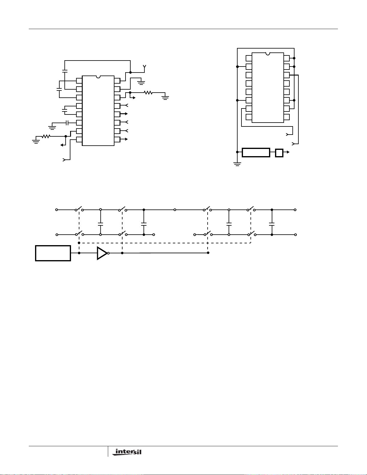
Test Circuits (HIN232E)
0.1µF
C3
0.1µF
C1
0.1µF
C2
3kΩ
T2
OUTPUT
RS-232
±30V INPUT
V
CC
GND
-
+
+
-
+
-
+
0.1µF C4
+4.5V TO
+5.5V INPUT
OUT
IN
T1
R1
R2
V
CC
GND
OUT
R1
OUT
T1
T2
OUT
16
15
14
13
IN
12
11
IN
10
IN
9
3kΩ
T1 OUTPUT
RS-232 ±30V INPUT
TTL/CMOS OUTPUT
TTL/CMOS INPUT
TTL/CMOS INPUT
TTL/CMOS OUTPUT
C1+
1
V+
2
C1-
3
C2+
4
C2-
5
-
V-
6
T2
7
8
R2
R
OUT
C1+
1
V+
2
C1-
3
C2+
4
C2-
5
V-
6
T2
7
R2
8
= VIN/I
V
= ±2V
IN
OUT
IN
T1
R1
R2
V
GND
OUT
R1
OUT
T1
T2
OUT
T2
CC
IN
IN
IN
OUT
T1
A
16
15
14
13
12
11
10
9
OUT
FIGURE 1. GENERAL TEST CIRCUIT FIGURE 2. POWER-OFF SOURCE RESISTANCE
CONFIGURATION
VOLTAGE DOUBLER
S1
S3
C1+
C1
S2
+
C1
-
-
S4
+
C3
-
V+ = 2V
CC
V
CC
GND
VOLTAGE INVERTER
S5
S7
C2+
C2-
S6
+
C2
-
S8
+
C4
-
GND
- = - (V+)
V
RC
OSCILLATOR
FIGURE 3. CHARGE PUMP
Detailed Description
The HIN2XXE family of high-speed RS-232
transmitters/receivers are powered by a single +5V power
supply, feature low power consumption, and meet all ElA
RS232C and V.28 specifications. The circuit is divided into
three sections: the charge pump, transmitter, and receiver.
Charge Pump
An equivalent circuit of the charge pump is illustrated in
Figure 3. The charge pump contains two sections: the
voltage doubler and the voltage inverter. Each section is
driven by a two phase, internally generated clock to
generate +10V and -10V. The nominal clock frequency is
125kHz. During phase one of the clock, capacitor C1 is
charged to V
added to V
V
. During phase two, C2 is also charged to 2VCC, and
CC
then during phase one, it is inverted with respect to ground
to produce a signal across C4 equal to -2V
pump accepts input voltages up to 5.5V. The output
. During phase two, the voltage on C1 is
CC
, producing a signal across C3 equal to twice
CC
. The charge
CC
impedance of the voltage doubler section (V+) is
approximately 200Ω, and the output impedance of the
voltage inverter section (V-) is approximately 450Ω. A typical
application uses 0.1µF capacitors for C1-C4, however, the
value is not critical. Increasing the values of C1 and C2 will
lower the output impedance of the voltage doubler and
inverter, increasing the values of the reservoir capacitors, C3
and C4, lowers the ripple on the V+ and V- supplies.
During shutdown mode (HIN206E, HIN211E and HIN213E)
the charge pump is turned off, V+ is pulled down to V
CC
, V-
is pulled up to GND, and the supply current is reduced to
less than 10µA. The transmitter outputs are disabled and the
receiver outputs (except for HIN213E, R4 and R5) are
placed in the high impedance state.
Transmitters
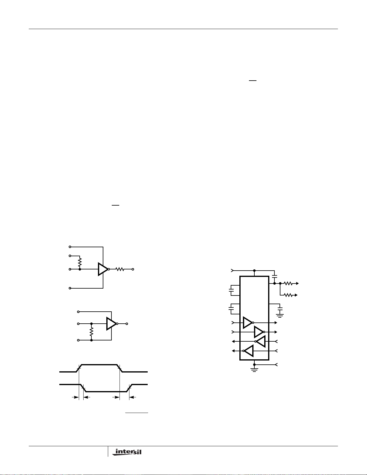
The transmitters are TTL/CMOS compatible inverters which
translate the inputs to RS-232 outputs. The input logic
threshold is about 26% of V
1 at the input results in a voltage of between -5V and V- at
, or 1.3V for VCC = 5V. A logic
CC
9
Page 10
HIN202E, HIN206E, HIN207E, HIN208E, HIN211E, HIN213E, HIN232E
the output, and a logic 0 results in a voltage between +5V
and (V+ -0.6V). Each transmitter input has an internal 400kΩ
pullup resistor so any unused input can be left unconnected
and its output remains in its low state. The output voltage
swing meets the RS-232C specifications of ±5V minimum
with the worst case conditions of: all transmitters driving 3kΩ
minimum load impedance, V
= 4.5V, and maximum
CC
allowable operating temperature. The transmitters have an
internally limited output slew rate which is less than 30V/µs.
The outputs are short circuit protected and can be shorted to
ground indefinitely. The powered down output impedance is
a minimum of 300Ω with ±2V applied to the outputs and
V
= 0V.
CC
Receivers
The receiver inputs accept up to ±30V while presenting the
required 3kΩ to 7kΩ input impedance even if the power is off
(V
= 0V). The receivers have a typical input threshold of
CC
1.3V which is within the ±3V limits, known as the transition
region, of the RS-232 specifications. The receiver output is
0V to V
greater than 2.4V and high whenever the input is floating or
driven between +0.8V and -30V. The receivers feature 0.5V
hysteresis (except during shutdown) to improve noise
rejection. The receiver Enable line EN
when unasserted, disables the receiver outputs, placing
them in the high impedance mode. The receiver outputs are
also placed in the high impedance state when in shutdown
mode (except HIN213E R4 and R5).
. The output will be low whenever the input is
CC
, (EN on HIN213E)
V+
V
GND < T
-30V < R
T
IN
OR
R
IN
T
OUT
OR
R
OUT
CC
T
XIN
XIN
V-
XIN
t
PHL
< V
400kΩ
CC
300Ω
FIGURE 4. TRANSMITTER
V
CC
R
XIN
< +30V
GND
5kΩ
GND < V
FIGURE 5. RECEIVER
t
PLH
V- < V
R
ROUT
OUT
T
OUT
TOUT
< V
< V+
CC
V
V
OL
OL
HIN213E Operation in Shutdown
The HIN213E features two receivers, R4 and R5, which
remain active in shutdown mode. During normal operation
the receivers propagation delay is typically 0.5µs. This
propagation delay may increase slightly during shutdown.
When entering shut down mode, receivers R4 and R5 are
not valid for 80µs after SD
= VIL. When exiting shutdown
mode, all receiver outputs will be invalid until the charge
pump circuitry reaches normal operating voltage. This is
typically less than 2ms when using 0.1µF capacitors.
Application Information
The HIN2XXE may be used for all RS-232 data terminal and
communication links. It is particularly useful in applications
where ±12V power supplies are not available for
conventional RS-232 interface circuits. The applications
presented represent typical interface configurations.
A simple duplex RS-232 port with CTS/RTS handshaking is
illustrated in Figure 7. Fixed output signals such as DTR
(data terminal ready) and DSRS (data signaling rate select)
is generated by driving them through a 5kΩ resistor
connected to V+.
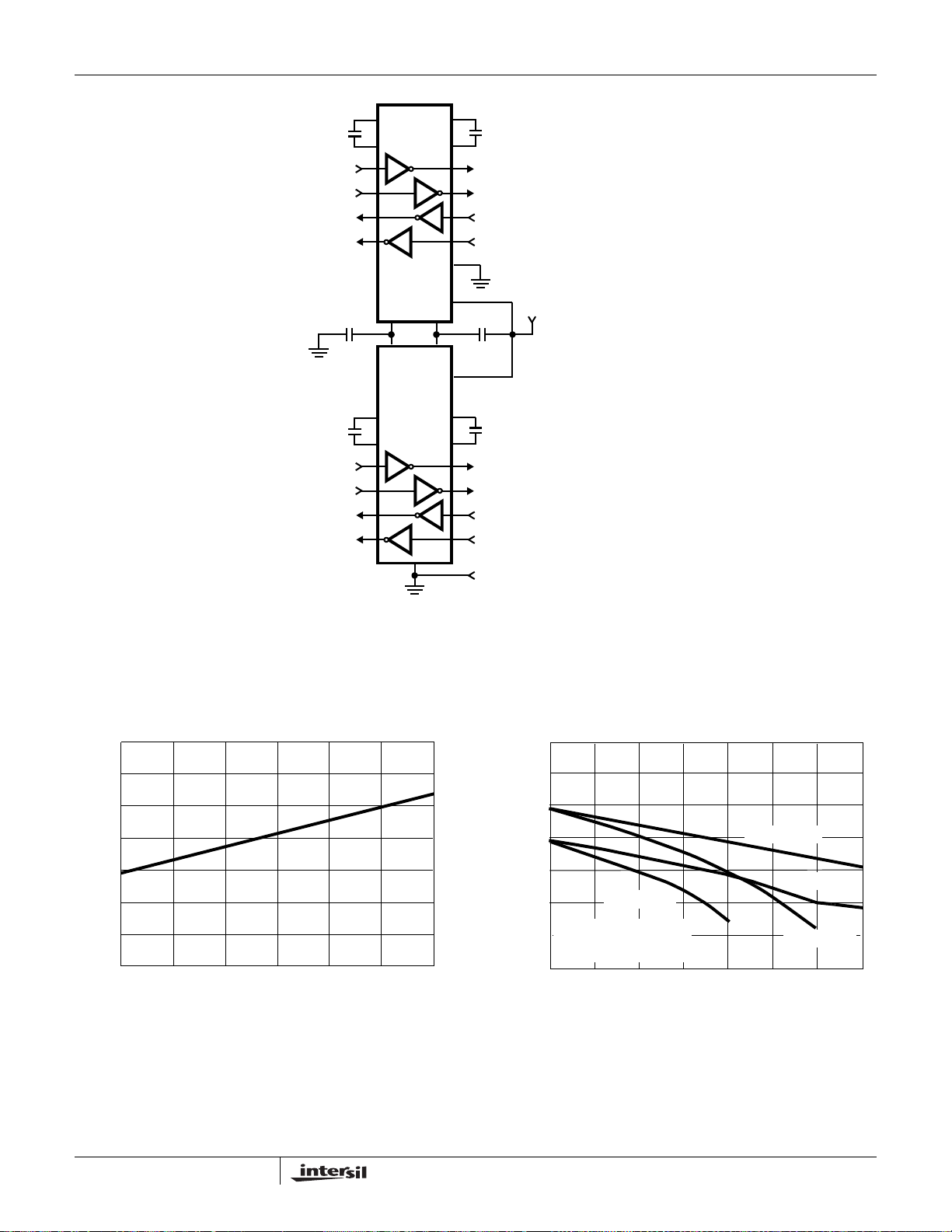
In applications requiring four RS-232 inputs and outputs
(Figure 8), note that each circuit requires two charge pump
capacitors (C1 and C2) but can share common reservoir
capacitors (C3 and C4). The benefit of sharing common
reservoir capacitors is the elimination of two capacitors and
the reduction of the charge pump source impedance which
effectively increases the output swing of the transmitters.
+5V
16
1
+
C1
C2
TD
RTS
RD
CTS
3
-
+
-
11
10
12
4
5
9
HIN232E
T1
R2
R1
0.1µF
0.1µF
INPUTS
OUTPUTS
TTL/CMOS
FIGURE 7. SIMPLE DUPLEX RS-232 PORT WITH CTS/RTS
HANDSHAKING
T2
-
+
6
-
+
14
TD (2) TRANSMIT DATA
7
RTS (4) REQUEST TO SEND
13
RD (3) RECEIVE DATA
8
CTS (5) CLEAR TO SEND
SIGNAL GROUND (7)15
CTR (20) DATA
TERMINAL READY
DSRS (24) DATA
SIGNALING RATE
SELECT
RS-232
INPUTS AND OUTPUTS
t
AVERAGE PROPAGATION DELAY =
PHL + tPLH
2
FIGURE 6. PROPAGATION DELAY DEFINITION
10
Page 11
HIN202E, HIN206E, HIN207E, HIN208E, HIN211E, HIN213E, HIN232E
INPUTS
OUTPUTS
TTL/CMOS
INPUTS
OUTPUTS
TTL/CMOS
C1
0.1µF
C1
0.1µF
DSRS
TD
RTS
RD
CTS
0.2µF
DTR
DCD
R1
R1
R1
T2
T2
4
+
C2
5
0.1µF
-
14
TD (2) TRANSMIT DATA
7
RTS (4) REQUEST TO SEND
13
RD (3) RECEIVE DATA
8
CTS (5) CLEAR TO SEND
15
V
16
26
2
CC
C3
+
-
0.2µF
V
16
CC
4
+
C2
5
0.1µF
-
14
DTR (20) DATA TERMINAL READY
7
DSRS (24) DATA SIGNALING RATE SELECT
13
DCD (8) DATA CARRIER DETECT
8
R1 (22) RING INDICATOR
+5V
RS-232
INPUTS AND OUTPUTS
1
+
C4
+
+
HIN232E
3
-
-
T1
11
10
12
R2
9
-
V- V+
6
HIN232E
1
3
T1
11
10
12
R2
9
FIGURE 8. COMBINING TWO HIN232Es FOR 4 PAIRS OF RS-232 INPUTS AND OUTPUTS
Typical Performance Curves
12
10
8
6
4
V- SUPPLY VOLTAGE (V)
2
0
3.5 4.0 4.5 6.0
V
CC
SIGNAL GROUND (7)15
0.1µF
5.0 5.53.0
12
10
8
6
4
SUPPLY VOLTAGE (|V|)
TA = 25oC
2
TRANSMITTER OUTPUTS
OPEN CIRCUIT
0
V- (VCC = 4V)
|I
LOAD
| (mA)
V+ (VCC = 5V)
V+ (VCC = 4V)
V- (VCC = 5V)
302520151050
35
FIGURE 9. V- SUPPLY VOLTAGE vs V
11
CC
FIGURE 10. V+, V- OUTPUT VOLTAGE vs LOAD
Page 12
HIN202E, HIN206E, HIN207E, HIN208E, HIN211E, HIN213E, HIN232E
Die Characteristics
DIE DIMENSIONS:
128 mils x 77 mils
METALLIZATION:
Type: Al
Thickness: 10k
Å ±1kÅ
SUBSTRATE POTENTIAL
GND
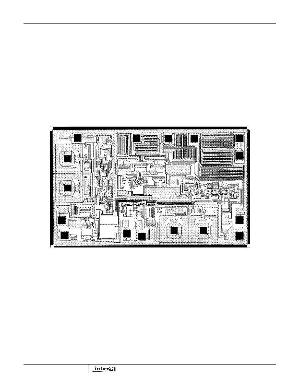
Metallization Mask Layout
V-
PIN 6
PIN 7
T2
OUT
C2-
PIN 5
HIN232E
PAS SIVATI ON:
Type: Nitride over Silox
Nitride Thickness: 8k
Silox Thickness: 7kÅ
TRANSISTOR COUNT:
185
PROCESS:
CMOS Metal Gate
C2+
PIN 4
C1-
PIN 3
Å
PIN 2 V+
PIN 1 C1+
IN
OUT
OUT
PIN 8R2
PIN 9T3
PIN 10R2
PIN 11
T2
IN
PIN 12
T1
IN
PIN 13
R1
OUT
PIN 14
R1
IN
PIN 15
T1
OUT
PIN 16
GND
PIN 17 V
CC
12
Page 13
HIN202E, HIN206E, HIN207E, HIN208E, HIN211E, HIN213E, HIN232E
Dual-In-Line Plastic Packages (PDIP)
N
D1
-C-
E1
-B-
A1
A2
E
A
L
e
C
C
L
e
A
C
e
B
INDEX
AREA
BASE
PLANE
SEATING
PLANE
D1
B1
12 3 N/2
-AD
e
B
0.010 (0.25) C AM BS
NOTES:
1. Controlling Dimensions: INCH. In case of conflict between English and
Metric dimensions, the inch dimensions control.
2. Dimensioning and tolerancing per ANSI Y14.5M-1982.
3. Symbols are defined in the “MO Series Symbol List” in Section 2.2 of
Publication No. 95.
4. Dimensions A, A1 and L are measured with the package seated in JEDEC seating plane gauge GS-3.
5. D, D1, and E1 dimensions do not include mold flash or protrusions.
Mold flash or protrusions shall not exceed 0.010 inch (0.25mm).
6. E and are measured with the leads constrained to be perpendic-
7. e
e
A
ular to datum .
and eC are measured at the lead tips with the leads unconstrained.
B
e
must be zero or greater.
C
-C-
8. B1 maximum dimensions do not include dambar protrusions. Dambar
protrusions shall not exceed 0.010 inch (0.25mm).
9. N is the maximum number of terminal positions.
10. Corner leads (1, N, N/2 and N/2 + 1) for E8.3, E16.3, E18.3, E28.3,
E42.6 will have a B1 dimension of 0.030 - 0.045 inch (0.76 - 1.14mm).
E16.3 (JEDEC MS-001-BB ISSUE D)
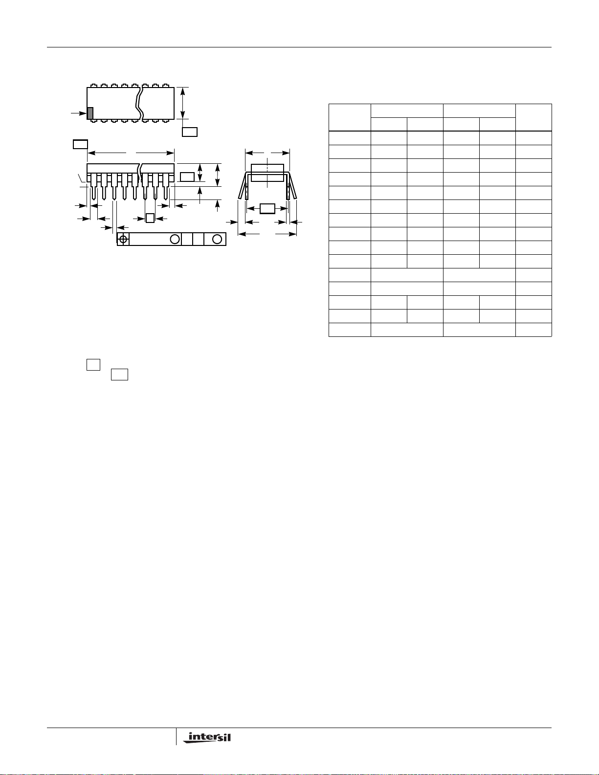
16 LEAD DUAL-IN-LINE PLASTIC PACKAGE
INCHES MILLIMETERS
SYMBOL
A - 0.210 - 5.33 4
A1 0.015 - 0.39 - 4
A2 0.115 0.195 2.93 4.95 -
B 0.014 0.022 0.356 0.558 -
B1 0.045 0.070 1.15 1.77 8, 10
C 0.008 0.014 0.204 0.355 -
D 0.735 0.775 18.66 19.68 5
D1 0.005 - 0.13 - 5
E 0.300 0.325 7.62 8.25 6
E1 0.240 0.280 6.10 7.11 5
e 0.100 BSC 2.54 BSC -
e
A
e
B
0.300 BSC 7.62 BSC 6
- 0.430 - 10.92 7
L 0.115 0.150 2.93 3.81 4
N16 169
NOTESMIN MAX MIN MAX
Rev. 0 12/93
13
Page 14
HIN202E, HIN206E, HIN207E, HIN208E, HIN211E, HIN213E, HIN232E
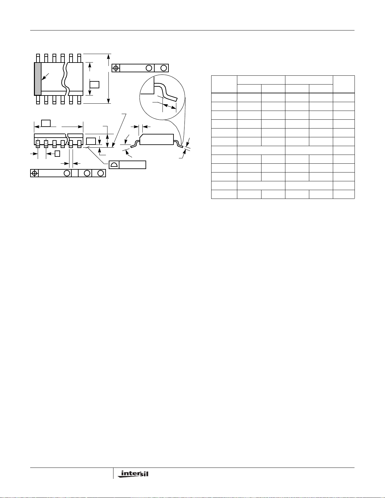
Small Outline Plastic Packages (SOIC)
N
INDEX
AREA
123
SEATING PLANE
-AD
e
B
0.25(0.010) C AM BS
M
E
-B-
A
-C-
0.25(0.010) BM M
H
α
µ
A1
0.10(0.004)
L
h x 45
o
C
NOTES:
1. Symbols are defined in the “MO Series Symbol List” in Section 2.2 of
Publication Number 95.
2. Dimensioning and tolerancing per ANSI Y14.5M-1982.
3. Dimension “D” does not include mold flash, protrusions or gate burrs.
Mold flash, protrusion and gate burrs shall not exceed 0.15mm (0.006
inch) per side.
4. Dimension “E” does not include interlead flash or protrusions. Interlead
flash and protrusions shall not exceed 0.25mm (0.010 inch) per side.
5. The chamfer on the body is optional. If it is not present, a visual index
feature must be located within the crosshatched area.
6. “L” is the length of terminal for soldering to a substrate.
7. “N” is the number of terminal positions.
8. Terminal numbers are shown for reference only.
9. The lead width “B”, as measured 0.36mm (0.014 inch) or greater above
the seating plane, shall not exceed a maximum value of 0.61mm
(0.024 inch).
10. Controlling dimension: MILLIMETER. Converted inch dimensions are
not necessarily exact.
M16.15 (JEDEC MS-012-AC ISSUE C)
16 LEAD NARROW BODY SMALL OUTLINE PLASTIC
PACKAGE
INCHES MILLIMETERS
SYMBOL
A 0.0532 0.0688 1.35 1.75 -
A1 0.0040 0.0098 0.10 0.25 -
B 0.013 0.020 0.33 0.51 9
C 0.0075 0.0098 0.19 0.25 -
D 0.3859 0.3937 9.80 10.00 3
E 0.1497 0.1574 3.80 4.00 4
e 0.050 BSC 1.27 BSC -
H 0.2284 0.2440 5.80 6.20 -
h 0.0099 0.0196 0.25 0.50 5
L 0.016 0.050 0.40 1.27 6
N16 167
o
α
0
o
8
o
0
o
8
Rev. 0 12/93
NOTESMIN MAX MIN MAX
-
14
Page 15
HIN202E, HIN206E, HIN207E, HIN208E, HIN211E, HIN213E, HIN232E
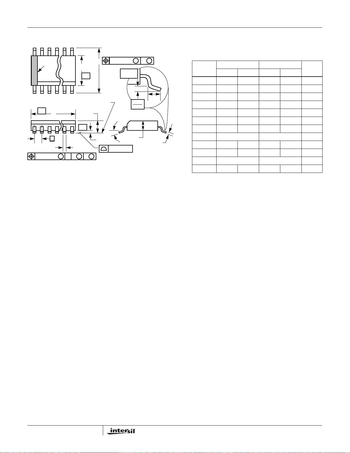
Small Outline Plastic Packages (SSOP)
N
INDEX
AREA
123
SEATING PLANE
-AD
e
B
0.25(0.010) C AM BS
M
E
-B-
A
-C-
0.25(0.010) BM M
H
α
µ
A1
0.10(0.004)
GAUGE
PLANE
0.25
0.010
A2
L
C
NOTES:
1. Symbols are defined in the “MO Series Symbol List” in Section 2.2 of
Publication Number 95.
2. Dimensioning and tolerancing per ANSI Y14.5M-1982.
3. Dimension “D” does not include mold flash, protrusions or gate burrs.
Mold flash, protrusion and gate burrs shall not exceed 0.20mm (0.0078
inch) per side.
4. Dimension “E” does not include interlead flash or protrusions. Interlead
flash and protrusions shall not exceed 0.20mm (0.0078 inch) per side.
5. The chamfer on the body is optional. If it is not present, a visual index
feature must be located within the crosshatched area.
6. “L” is the length of terminal for soldering to a substrate.
7. “N” is the number of terminal positions.
8. Terminal numbers are shown for reference only.
9. Dimension “B” does not include dambar protrusion. Allowable dambar
protrusion shall be 0.13mm (0.005 inch) total in excess of “B” dimension at maximum material condition.
10. Controlling dimension: MILLIMETER. Converted inch dimensions are
not necessarily exact.
M16.209 (JEDEC MO-150-AC ISSUE B)
16 LEAD SHRINK SMALL OUTLINE PLASTIC PACKAGE
INCHES MILLIMETERS
SYMBOL
A - 0.078 - 2.00 -
A1 0.002 - 0.05 - -
A2 0.065 0.072 1.65 1.85 -
B 0.009 0.014 0.22 0.38 9
C 0.004 0.009 0.09 0.25 -
D 0.233 0.255 5.90 6.50 3
E 0.197 0.220 5.00 5.60 4
e 0.026 BSC 0.65 BSC -
H 0.292 0.322 7.40 8.20 -
L 0.022 0.037 0.55 0.95 6
N16 167
o
α
0
o
8
o
0
NOTESMIN MAX MIN MAX
o
8
Rev. 2 3/95
-
15
Page 16
HIN202E, HIN206E, HIN207E, HIN208E, HIN211E, HIN213E, HIN232E
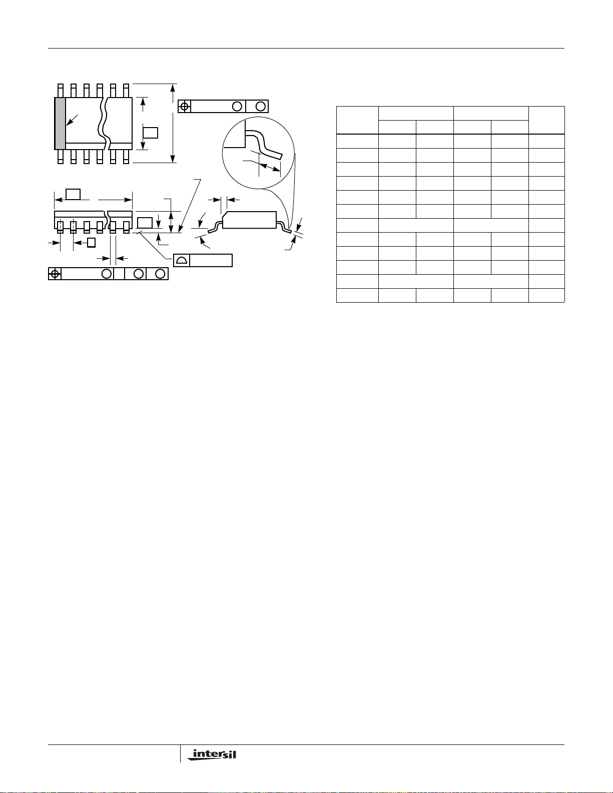
Small Outline Plastic Packages (SOIC)
N
INDEX
AREA
123
SEATING PLANE
-AD
e
B
0.25(0.010) C AM BS
M
E
-B-
A
-C-
0.25(0.010) BM M
H
α
µ
A1
0.10(0.004)
L
h x 45
o
C
NOTES:
1. Symbols are defined in the “MO Series Symbol List” in Section 2.2 of
Publication Number 95.
2. Dimensioning and tolerancing per ANSI Y14.5M-1982.
3. Dimension “D” does not include mold flash, protrusions or gate burrs.
Mold flash, protrusion and gate burrs shall not exceed 0.15mm (0.006
inch) per side.
4. Dimension “E” does not include interlead flash or protrusions. Interlead
flash and protrusions shall not exceed 0.25mm (0.010 inch) per side.
5. The chamfer on the body is optional. If it is not present, a visual index
feature must be located within the crosshatched area.
6. “L” is the length of terminal for soldering to a substrate.
7. “N” is the number of terminal positions.
8. Terminal numbers are shown for reference only.
9. The lead width “B”, as measured 0.36mm (0.014 inch) or greater above
the seating plane, shall not exceed a maximum value of 0.61mm (0.024
inch)
10. Controlling dimension: MILLIMETER. Converted inch dimensions are
not necessarily exact.
M16.3 (JEDEC MS-013-AA ISSUE C)
16 LEAD WIDE BODY SMALL OUTLINE PLASTIC PACKAGE
INCHES MILLIMETERS
SYMBOL
A 0.0926 0.1043 2.35 2.65 -
A1 0.0040 0.0118 0.10 0.30 -
B 0.013 0.0200 0.33 0.51 9
C 0.0091 0.0125 0.23 0.32 -
D 0.3977 0.4133 10.10 10.50 3
E 0.2914 0.2992 7.40 7.60 4
e 0.050 BSC 1.27 BSC -
H 0.394 0.419 10.00 10.65 -
h 0.010 0.029 0.25 0.75 5
L 0.016 0.050 0.40 1.27 6
N16 167
o
α
0
o
8
o
0
o
8
Rev. 0 12/93
NOTESMIN MAX MIN MAX
-
16
Page 17
HIN202E, HIN206E, HIN207E, HIN208E, HIN211E, HIN213E, HIN232E
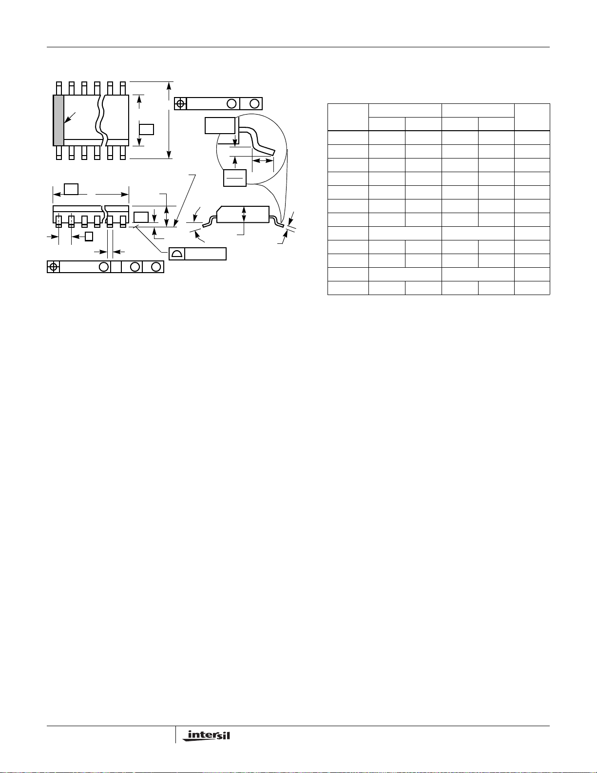
Shrink Small Outline Plastic Packages (SSOP)
N
INDEX
AREA
123
SEATING PLANE
-AD
e
B
0.25(0.010) C AM BS
M
E
-B-
A
-C-
0.25(0.010) BM M
H
α
µ
A1
0.10(0.004)
GAUGE
PLANE
0.25
0.010
A2
L
C
NOTES:
1. Symbols are defined in the “MO Series Symbol List” in Section 2.2 of
Publication Number 95.
2. Dimensioning and tolerancing per ANSI Y14.5M-1982.
3. Dimension “D” does not include mold flash, protrusions or gate burrs.
Mold flash, protrusion and gate burrs shall not exceed 0.20mm
(0.0078 inch) per side.
4. Dimension “E” does not include interlead flash or protrusions. Interlead flash and protrusions shall not exceed 0.20mm (0.0078 inch) per
side.
5. The chamfer on the body is optional. If it is not present, a visual index
feature must be located within the crosshatched area.
6. “L” is the length of terminal for soldering to a substrate.
7. “N” is the number of terminal positions.
8. Terminal numbers are shown for reference only.
9. Dimension “B” does not include dambar protrusion. Allowable dambar
protrusion shall be 0.13mm (0.005 inch) total in excess of “B” dimension at maximum material condition.
10. Controlling dimension: MILLIMETER. Converted inch dimensions
are not necessarily exact.
M24.209 (JEDEC MO-150-AG ISSUE B)
24 LEAD SHRINK SMALL OUTLINE PLASTIC PACKAGE
INCHES MILLIMETERS
SYMBOL
A - 0.078 - 2.00 -
A1 0.002 - 0.05 - -
A2 0.065 0.072 1.65 1.85 -
B 0.009 0.014 0.22 0.38 9
C 0.004 0.009 0.09 0.25 -
D 0.312 0.334 7.90 8.50 3
E 0.197 0.220 5.00 5.60 4
e 0.026 BSC 0.65 BSC -
H 0.292 0.322 7.40 8.20 -
L 0.022 0.037 0.55 0.95 6
N24 247
o
α
0
o
8
o
0
NOTESMIN MAX MIN MAX
o
8
Rev. 1 3/95
-
17
Page 18
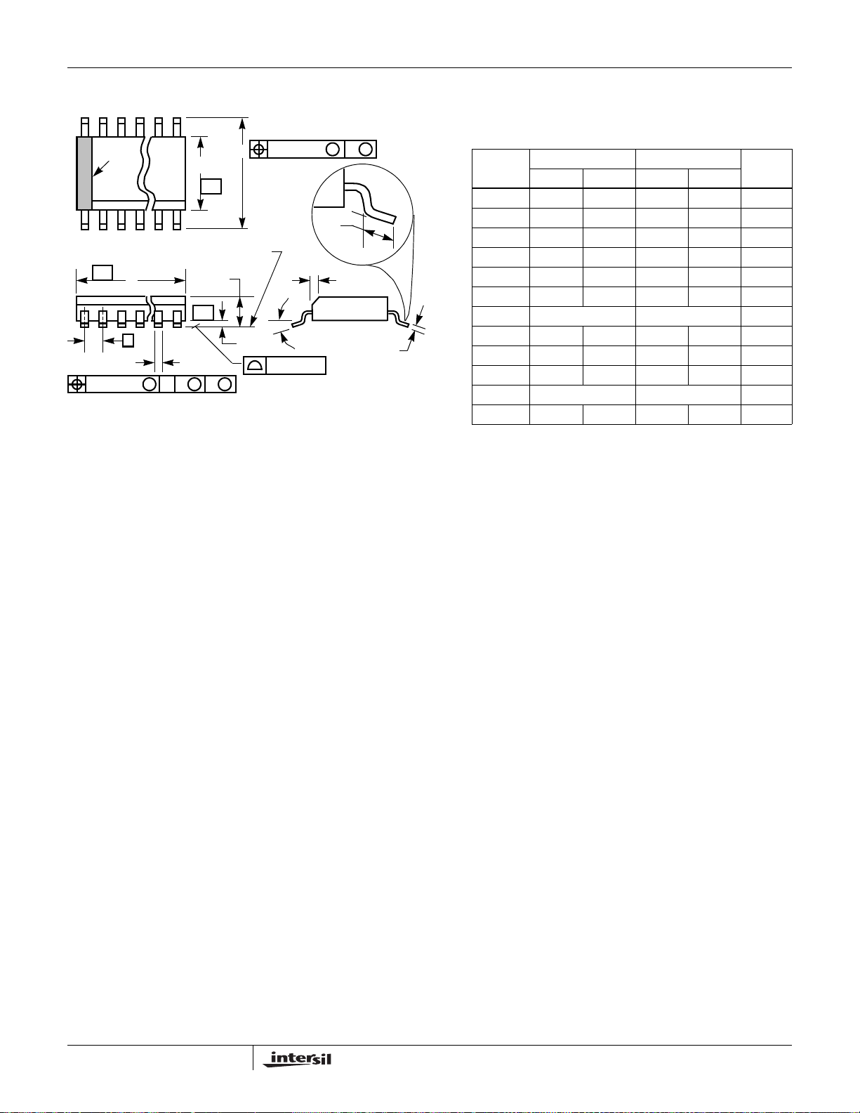
HIN202E, HIN206E, HIN207E, HIN208E, HIN211E, HIN213E, HIN232E
Small Outline Plastic Packages (SOIC)
N
INDEX
AREA
123
SEATING PLANE
-AD
e
B
0.25(0.010) C AM BS
M
E
-B-
A
-C-
0.25(0.010) BM M
H
α
µ
A1
0.10(0.004)
L
h x 45
o
C
NOTES:
1. Symbols are defined in the “MO Series Symbol List” in Section 2.2 of
Publication Number 95.
2. Dimensioning and tolerancing per ANSI Y14.5M-1982.
3. Dimension “D” does not include mold flash, protrusions or gate burrs.
Mold flash, protrusion and gate burrs shall not exceed 0.15mm
(0.006 inch) per side.
4. Dimension “E” does not include interlead flash or protrusions. Interlead flash and protrusions shall not exceed 0.25mm (0.010 inch) per
side.
5. The chamfer on the body is optional. If it is not present, a visual index
feature must be located within the crosshatched area.
6. “L” is the length of terminal for soldering to a substrate.
7. “N” is the number of terminal positions.
8. Terminal numbers are shown for reference only.
9. The lead width “B”, as measured 0.36mm (0.014 inch) or greater
above the seating plane, shall not exceed a maximum value of
0.61mm (0.024 inch)
10. Controlling dimension: MILLIMETER. Converted inch dimensions
are not necessarily exact.
M24.3 (JEDEC MS-013-AD ISSUE C)
24 LEAD WIDE BODY SMALL OUTLINE PLASTIC PACKAGE
INCHES MILLIMETERS
SYMBOL
A 0.0926 0.1043 2.35 2.65 -
A1 0.0040 0.0118 0.10 0.30 -
B 0.013 0.020 0.33 0.51 9
C 0.0091 0.0125 0.23 0.32 -
D 0.5985 0.6141 15.20 15.60 3
E 0.2914 0.2992 7.40 7.60 4
e 0.05 BSC 1.27 BSC -
H 0.394 0.419 10.00 10.65 -
h 0.010 0.029 0.25 0.75 5
L 0.016 0.050 0.40 1.27 6
N24 247
o
α
0
o
8
o
0
o
8
Rev. 0 12/93
NOTESMIN MAX MIN MAX
-
18
Page 19
HIN202E, HIN206E, HIN207E, HIN208E, HIN211E, HIN213E, HIN232E
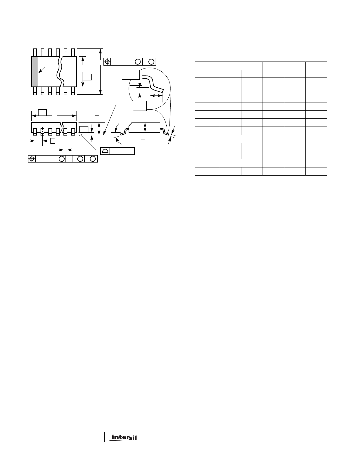
Shrink Small Outline Plastic Packages (SSOP)
N
INDEX
AREA
123
SEATING PLANE
-AD
e
B
0.25(0.010) C AM BS
M
E
-B-
A
-C-
0.25(0.010) BM M
H
α
µ
A1
0.10(0.004)
GAUGE
PLANE
0.25
0.010
A2
L
C
NOTES:
1. Symbols are defined in the “MO Series Symbol List” in Section 2.2
of Publication Number 95.
2. Dimensioning and tolerancing per ANSI Y14.5M-1982.
3. Dimension “D” does not include mold flash, protrusions or gate
burrs. Mold flash, protrusion and gate burrs shall not exceed
0.20mm (0.0078 inch) per side.
4. Dimension “E” does not include interlead flash or protrusions. Interlead flash and protrusions shall not exceed 0.20mm (0.0078 inch)
per side.
5. The chamfer on the body is optional. If it is not present, a visual index feature must be located within the crosshatched area.
6. “L” is the length of terminal for soldering to a substrate.
7. “N” is the number of terminal positions.
8. Terminal numbers are shown for reference only.
9. Dimension “B” does not include dambar protrusion. Allowable dambar protrusion shall be 0.13mm (0.005 inch) total in excess of “B”
dimension at maximum material condition.
10. Controlling dimension: MILLIMETER. Converted inch dimensions
are not necessarily exact.
M28.209 (JEDEC MO-150-AH ISSUE B)
28 LEAD SHRINK SMALL OUTLINE PLASTIC PACKAGE
INCHES MILLIMETERS
SYMBOL
A - 0.078 - 2.00 -
A1 0.002 - 0.05 - -
A2 0.065 0.072 1.65 1.85 -
B 0.009 0.014 0.22 0.38 9
C 0.004 0.009 0.09 0.25 -
D 0.390 0.413 9.90 10.50 3
E 0.197 0.220 5.00 5.60 4
e 0.026 BSC 0.65 BSC -
H 0.292 0.322 7.40 8.20 -
L 0.022 0.037 0.55 0.95 6
N28 287
o
α
0
o
8
o
0
o
8
Rev. 1 3/95
NOTESMIN MAX MIN MAX
-
19
Page 20
HIN202E, HIN206E, HIN207E, HIN208E, HIN211E, HIN213E, HIN232E
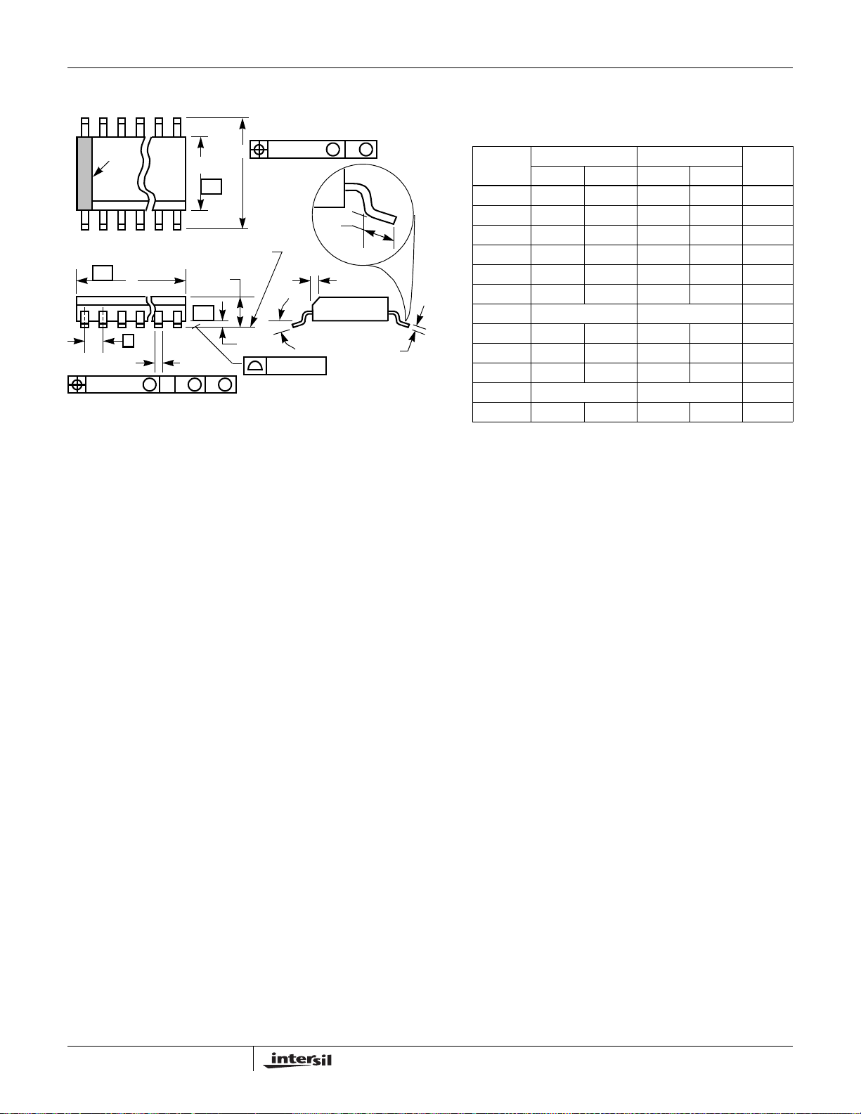
Small Outline Plastic Packages (SOIC)
N
INDEX
AREA
123
SEATING PLANE
-AD
e
B
0.25(0.010) C AM BS
M
E
-B-
A
-C-
0.25(0.010) BM M
H
α
µ
A1
0.10(0.004)
L
h x 45
o
NOTES:
1. Symbols are defined in the “MO Series Symbol List” in Section 2.2
of Publication Number 95.
2. Dimensioning and tolerancing per ANSI Y14.5M-1982.
3. Dimension “D” does not include mold flash, protrusions or gate
burrs. Mold flash, protrusion and gate burrs shall not exceed
0.15mm (0.006 inch) per side.
4. Dimension “E” does not include interlead flash or protrusions. Interlead flash and protrusions shall not exceed 0.25mm (0.010
inch) per side.
5. The chamfer on the body is optional. If it is not present, a visual
index feature must be located within the crosshatched area.
6. “L” is the length of terminal for soldering to a substrate.
7. “N” is the number of terminal positions.
8. Terminal numbers are shown for reference only.
9. The lead width “B”, as measured 0.36mm (0.014 inch) or greater
above the seating plane, shall not exceed a maximum value of
0.61mm (0.024 inch)
10. Controlling dimension: MILLIMETER. Converted inch dimensions are not necessarily exact.
M28.3 (JEDEC MS-013-AE ISSUE C)
28 LEAD WIDE BODY SMALL OUTLINE PLASTIC PACKAGE
INCHES MILLIMETERS
SYMBOL
A 0.0926 0.1043 2.35 2.65 -
A1 0.0040 0.0118 0.10 0.30 -
B 0.013 0.0200 0.33 0.51 9
C 0.0091 0.0125 0.23 0.32 -
D 0.6969 0.7125 17.70 18.10 3
E 0.2914 0.2992 7.40 7.60 4
e 0.05 BSC 1.27 BSC -
H 0.394 0.419 10.00 10.65 -
C
h 0.01 0.029 0.25 0.75 5
L 0.016 0.050 0.40 1.27 6
N28 287
o
α
0
o
8
o
0
o
8
Rev. 0 12/93
NOTESMIN MAX MIN MAX
-
20
Page 21
HIN202E, HIN206E, HIN207E, HIN208E, HIN211E, HIN213E, HIN232E
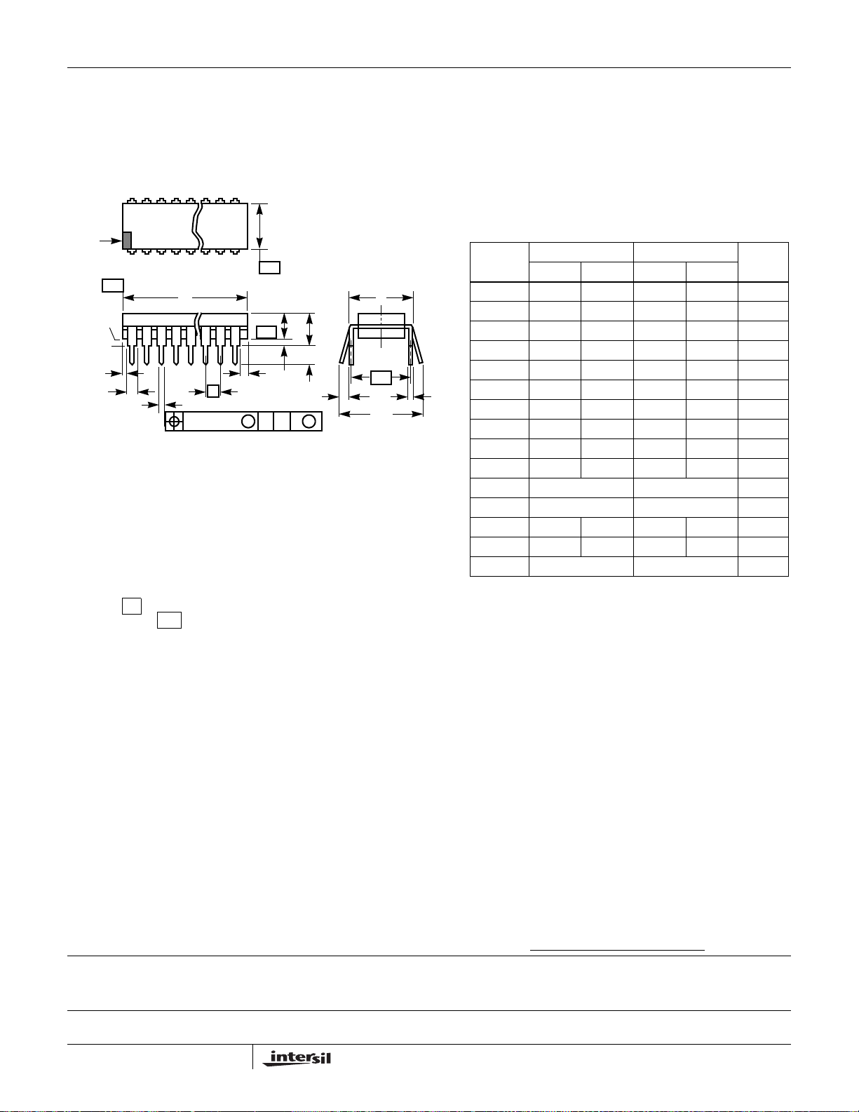
Dual-In-Line Plastic Packages (PDIP)
File Number
N
D1
-C-
E1
-B-
A1
A2
E
A
L
e
C
C
L
e
A
C
e
B
INDEX
AREA
BASE
PLANE
SEATING
PLANE
D1
B1
12 3 N/2
-AD
e
B
0.010 (0.25) C AM BS
NOTES:
1. Controlling Dimensions: INCH. In case of conflict between English and
Metric dimensions, the inch dimensions control.
2. Dimensioning and tolerancing per ANSI Y14.5M-1982.
3. Symbols are defined in the “MO Series Symbol List” in Section 2.2 of
Publication No. 95.
4. Dimensions A, A1 and L are measured with the package seated in
JEDEC seating plane gauge GS-3.
5. D, D1, and E1 dimensions do not include mold flash or protrusions.
Mold flash or protrusions shall not exceed 0.010 inch (0.25mm).
6. E and are measured with the leads constrained to be perpendic-
7. e
e
A
ular to datum .
and eC are measured at the lead tips with the leads unconstrained.
B
e
must be zero or greater.
C
-C-
8. B1 maximum dimensions do not include dambar protrusions. Dambar
protrusions shall not exceed 0.010 inch (0.25mm).
9. N is the maximum number of terminal positions.
10. Corner leads (1, N, N/2 and N/2 + 1) for E8.3, E16.3, E18.3, E28.3,
E42.6 will have a B1 dimension of 0.030 - 0.045 inch (0.76 - 1.14mm).
E24.3 (JEDEC MS-001-AF ISSUE D)
24 LEAD NARROW BODY DUAL-IN-LINE PLASTIC
PACKAGE
INCHES MILLIMETERS
SYMBOL
A - 0.210 - 5.33 4
A1 0.015 - 0.39 - 4
A2 0.115 0.195 2.93 4.95 -
B 0.014 0.022 0.356 0.558 -
B1 0.045 0.070 1.15 1.77 8
C 0.008 0.014 0.204 0.355 -
D 1.230 1.280 31.24 32.51 5
D1 0.005 - 0.13 - 5
E 0.300 0.325 7.62 8.25 6
E1 0.240 0.280 6.10 7.11 5
e 0.100 BSC 2.54 BSC -
e
A
e
B
0.300 BSC 7.62 BSC 6
- 0.430 - 10.92 7
L 0.115 0.150 2.93 3.81 4
N24 249
NOTESMIN MAX MIN MAX
Rev. 0 12/93
All Intersil products are manufactured, assembled and tested utilizing ISO9000 quality systems.
Intersil Corporation’s quality certifications can be viewed at website www.intersil.com/design/quality
Intersil products are sold by description only. Intersil Corporation reserves the right to make changes in circuit design and/or specifications at any time without notice.
Accordingly, the reader is cautioned to verify that data sheets are current before placing orders. Information furnished by Intersil is believed to be accurate and reliable. However, no responsibility is assumed by Intersil or its subsidiaries for its use; nor for any infringements of patents or other rights of third parties which may result from its use. No
license is granted by implication or otherwise under any patent or patent rights of Intersil or its subsidiaries.
For information regarding Intersil Corporation and its products, see web site www.intersil.com
21
 Loading...