

Intersil ISL54200EVAL1Z User Manual
®
ISL54200EVAL1Z Evaluation Board
User’s Manual
Application Note June 13, 2007
Description
The ISL54200EVAL1Z evaluation board is designed to
provide a quick and easy method for evaluating the
ISL54200 USB Switch IC.
The ISL54200 device is a unique IC. To use this evaluation
board properly requires a thorough knowledge of the
operation of the IC. Refer to the data sheet for an
understanding of the functions and features of the device.
Studying the device’s truth-table along with its pin-out
diagram on page 2 of the data sheet is the best way to get a
quick understanding of how the part works.
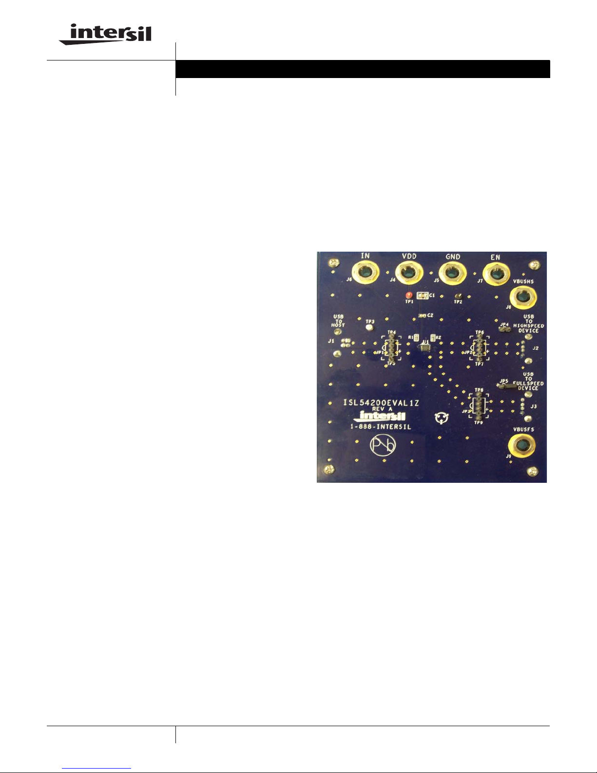
A picture of the main evaluation board is shown in Figure 1.
The ISL54200
board. It is located in the center of the board and is
designated as U1.
The evaluation board contains USB connectors to allow the
user to easily interface with the IC to evaluate its functions,
features, and performance. For example, with the board
properly powered and configured as shown in Figure 2 you
can control the logic pins, IN and EN, to switch between a
high-speed device and a full-speed device while connected
to a single USB host (computer).
μTQFN IC is soldered onto the evaluation
AN1330.0
Features
• Standard USB Connectors
• Standard Banana Jacks for Power, Ground, V
Logic Connections
• Jumpers to allow a device to be powered through the Host
Controller
• Convenient Test Points and Connections for Test
Equipment
BUS
and
Picture of Evaluation Board (Top View)
In a typical application, the ISL54200 dual SPDT device is
used to select between two different USB transceiver
sections of a media player. Logic control from a
determines which section to connect to the computer. To
change channels, the following sequence would possibly be
followed:
1. A signal would be sent to take the EN pin Low, to open all
switches. The off-isolation of the ISL54200 device would
allow the present active channel to properly disconnect
from the computer.
2. The IN pin would be set to select the other USB channel.
3. The EN pin would then be taken High to close the
switches to make the connection between the computer
and the other USB section of the player.
This application note will guide the user through the process
of configuring and using the evaluation board to evaluate the
ISL54200 device.
µprocessor
FIGURE 1. ISL54200EVAL1Z EVALUATION BOARD
1
CAUTION: These devices are sensitive to electrostatic discharge; follow proper IC Handling Procedures.
1-888-INTERSIL or 1-888-468-3774
| Intersil (and design) is a registered trademark of Intersil Americas Inc.
All other trademarks mentioned are the property of their respective owners.
Copyright Intersil Americas Inc. 2007. All Rights Reserved

Application Note 1330
Board Architecture/Layout
Basic Layout of Evaluation Board
The basic layout of the main board is as follows: Refer to
Figure 1.
• Power and Ground connections are at the top of the board
at banana jacks (J4 and J5).
• Logic connections, IN and EN, are at the top of the board
at banana jacks (J6 and J7).
• USB connection to an upstream host controller
(Computer) is made at J1, located on the left under-side of
the board.
• USB connections to downstream USB devices are made
at connectors J2 and J3, located on right under-side of the
board.
•V
• Located in the center of the board is the ISL54200 IC (U1).
IC Power Supply
A DC power supply connected at banana jacks J4 (VDD)
and J5 (GND) provides power to the ISL54200 IC. The IC
requires a 3.3VDC to 5VDC power supply for proper
operation. The power supply should be capable of delivering
100µA of current.
V
A DC power supply connected at banana jacks J8
(VBUSHS) and J9 (VBUSFS) provides the V
required by the USB devices. The devices require a DC
power supply in the range of 4.4V to 5.25V for proper
operation. The power supply should be capable of delivering
100µA of current.
The J8 banana jack is connected to the VBUS pin of the J2
“A” type USB receptacle. The J9 banana jack is connected
to the VBUS pin of the J3 “A” type receptacle.
The V
controller (computer) by installing a jumper at either JP4 or
JP5.
With a jumper at JP4, the V
to the J2 connector. With this jumper installed, no DC supply
should be connected at the J8 (VBUSHS) banana jack.
With a jumper at JP5, the V
to the J3 connector. With this jumper installed, no DC supply
should be connected at the J9 (VBUSFS) banana jack.
voltage for the USB devices are made through
BUS
banana jacks J8 and J9. Optionally, V
devices can be connected to the Host Controller V
for the USB
BUS
BUS
through jumpers JP4 and JP5.
The eval board has a pin 1 dot, to show how the IC should
be oriented on to the evaluation board. The IC pin 1
indicator dot needs to be aligned with the evaluation board
pin 1 dot indicator.
Power Supply
BUS
voltage
BUS
voltage can be provide from the USB host
BUS
voltage from J1 gets routed
BUS
voltage from J1 gets routed
BUS
Logic Control
The state of the ISL54200 device is determined by the
voltage at the IN pin and the EN pin. Access to the IN pin is
through the banana jack J6 (IN) and access to the EN pin is
through the banana jack J7 (EN).
If IN is driven Low (to ground) and EN = High (>1.4V), the
full-speed (FS) switches will be ON. In this state, the USB
host controller (computer) connected at J1 will be connected
through to the USB device connected at J3 and data will be
able to be transmitted between the computer and the device.
If IN is driven High (>1.4V) and EN = High (>1.4V), the
high-speed (HS) switches will be ON. In this state, the USB
host controller (computer) connected at J1 will be connected
through to the USB device connected at J2 and data will be
able to be transmitted between the computer and the device.
If EN = Low (driven to ground or floating), all switches will be
OFF. Neither device will be connected through to the host
controller.
In a typical application, the ISL54200 dual SPDT device is
used to select between two different USB transceiver
sections of a media player. Logic control from a
µprocessor
determines which section to connect to the computer. To
change channels, the following sequence would possibly be
followed:
1. A signal would be sent to take the EN pin Low, to open all
switches. The off-isolation of the ISL54200 device would
allow the present active channel to properly disconnect
from the computer.
2. Then the IN pin would be set to select the other USB
channel.
3. The EN pin would then be taken High to close the
switches to make the connection between the computer
and the other USB section of the player.
USB Connections
A “B” type USB receptacle labeled “USB TO HOST” (J1) is
located on the left under-side of the board. This receptacle
should be connected, using a standard USB cable, to the
upstream USB host controller, which is usually a PC
computer or hub. When this connection is made, the
ISL54200 device will connect the computer through to the
USB device determined by the voltage at the IN logic control
pin.
An “A” type USB receptacle labeled “USB TO HIGHSPEED
DEVICE” (J2) is located on the right under-side of the board.
The USB device can be plugged directly into this receptacle
or through a standard USB cable.
An “A” type USB receptacle labeled “USB TO FULLSPEED
DEVICE” (J3) is located on the right under-side of the board.
The USB device can be plugged directly into this receptacle
or through a standard USB cable.
2
AN1330.0
June 13, 2007
 Loading...