

Page 1

®
ISL41387EVAL1Z User’s Manual
Application Note May 30, 2006
Description
The ISL41387 evaluation board is RoHS compliant, and
provides a quick and easy method for evaluating this Dual
Protocol IC. The eval board also accommodates the
ISL41334; see the “ISL41334EVAL1Z User’s Manual” for
details.
This board was designed to allow the user to evaluate all the
features available on the ISL81387 and ISL41387 products.
The ISL41387 is the full featured version (see “Features”
below), where the QFN package’s increased pin count gives
the user access to functionality not available on the pin
limited ISL81387. The same die is used in both products, so
other than minor package effects, evaluating the QFN
packaged ISL41387 is a reasonable substitute for evaluating
the ISL81387.
By changing jumper positions the user can quickly set the
board to evaluate any of the ISL41387’s many modes and
features, and the input states can also be set via jumpers.
Refer to the data sheet for complete details regarding the
functions and features of this device. These dual protocol
ICs feature many modes, so studying the device’s truth-table
along with its operating circuits and detailed description is
the best way to gain an understanding of how the part works.
Features
• QFN Version Demonstrates All Enhanced Features:
Logic Supply Pin (VL)
Three RS-485 Speed Options - 115kbps/460kbps/20Mbps
Active Low RS-485 Rx Enable for Simple Direction Control
• Quick Configuration Using Jumpers
• State of All Inputs Can be Set by Jumper Positions
• No Bus Termination Resistors; Allows RS-232 or RS-485
Evaluation
• Simple Operation Requires Only One, 5V, Power Supply
Important Notes
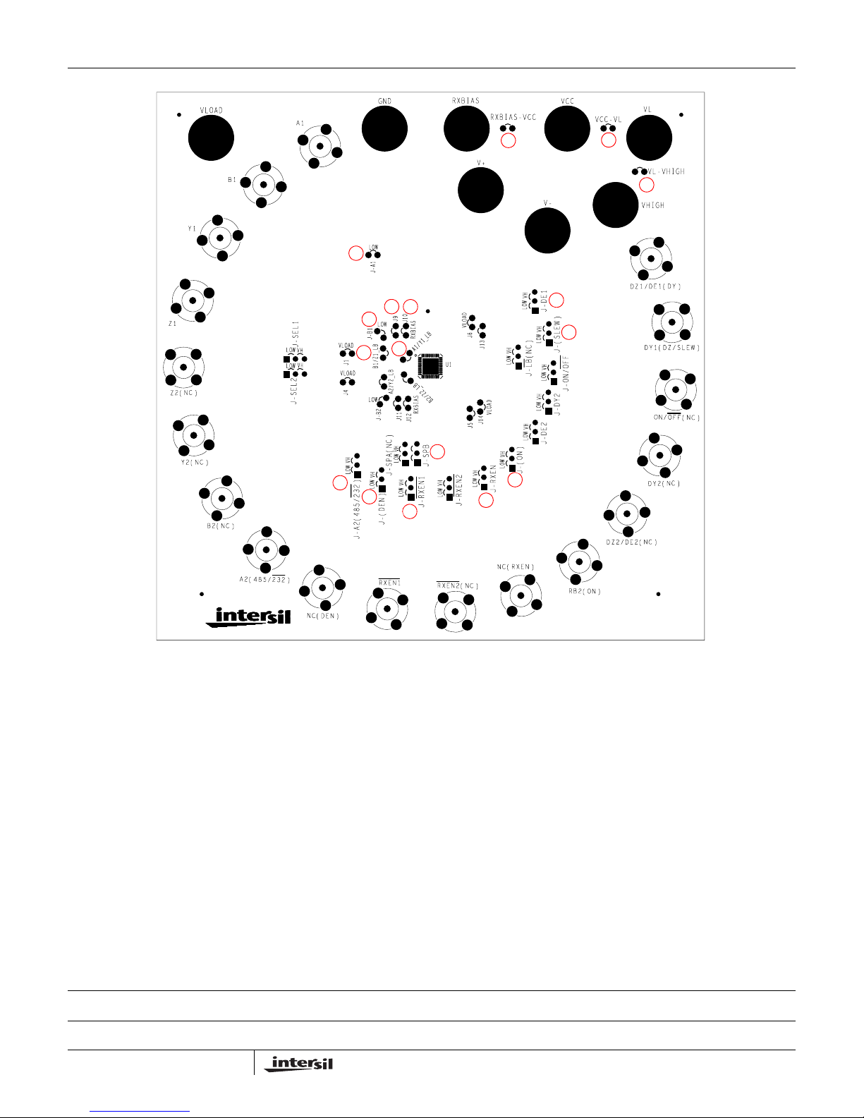
To facilitate locating jumpers on this board, Figure 3 is a
jumper locator and, in this Application Note, the (#) following
a jumper mention corresponds to the red jumper number on
the locator. See the “Jumper Definitions” section for a
description of the function of each jumper.
The base board is used to evaluate both the ISL41334
(2 port) and ISL41387 (1 port) products, so the jumper and
connector names reflect the functionality of both products.
Due to space limitations some jumper labels are
abbreviated, but the corresponding BNC connector has the
full label.
AN1248.1
In most cases, a name that applies to both products contains
no parenthesis (e.g., “B1”), a name that applies to only the
ISL41334 is followed by “(NC)” (e.g., “B2 (NC)”), and a name
that applies to only the ISL41387 is preceded by “NC” and/or
has the name in parenthesis (e.g., “NC (DEN)” or “(DEN)”).
Note that on “Rev . A” of these boards the following minor errors
have been noted, and are corrected on subsequ ent revisions:
• Jumper labels “J-SELX” (not numbered) should be
“J-SELX (NC)” because they are not used for the
ISL41387
• Jumper label “J-RXEN2
“J-RXEN2
• Jumper label “J-RXEN” (11) should be “J-(RXEN)”
because it is only used for the ISL41387
• Jumper label “J-DE2” (not numbered) should be “J-DE2
(NC)” because it is not used for the ISL41387
• Jumper label “J-DY2” (not numbered) should be “J-DY2
(NC)” because it is not used for the ISL41387
• Jumper label “J-ON/OFF
“J-ON/OFF
• Jumper label “J-(SLEW)” (13) should be “J-DY1 (SLEW)”
• Jumper label “J-DE1” (14) should be “J-DZ1/DE1 (DY)”.
It is important to note that the ISLX1387 don’t follow the
RS-485 convention whereby the inverting I/O is labeled
“B/Z”, and the noninverting I/O is “A/Y”. Thus, the 1387 A/Y
(B/Z) pins connect to the B/Z (A/Y) pins of generic
RS-485/422 ICs.
Input signals that are likely to be driven by a generator
connect to a BNC connector, and there is a 50Ω termination
resistor to GND when the jumper is in the “LOW” position.
(NC)” because it is not used for the ISL41387
(NC)” because it is not used for the ISL41387
” (not numbered) should be
” (not numbered) should be
Default Configuration
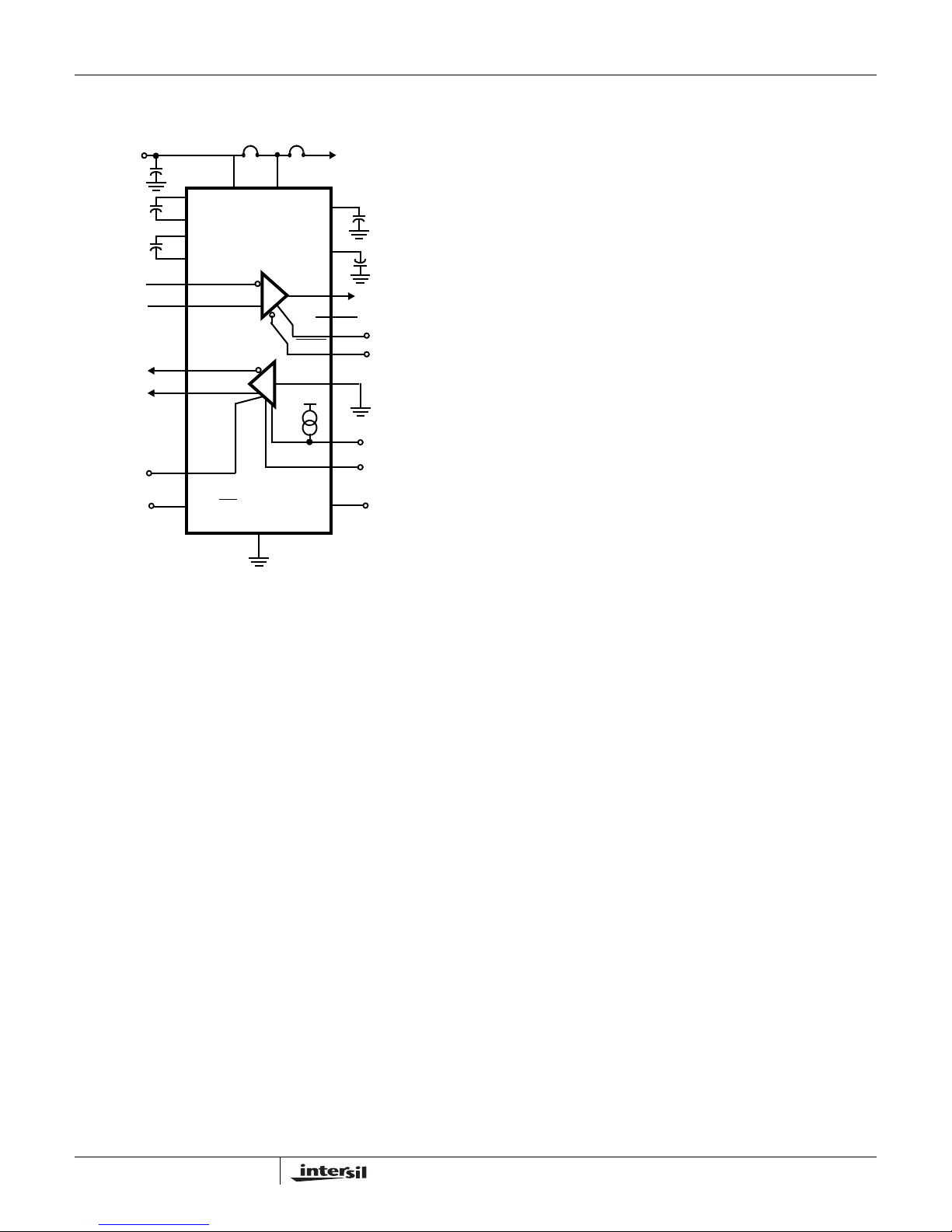
As delivered (see “Functional Diagram”), the board is
configured for powered-up (not SHDN) RS-485 mode, driver
enabled, via DEN, and set for high speed (20Mbps)
operation, driver input (DY) low, Rx enabled via the RXEN
line, Rx inputs floating, and V
this configuration, the jumpers are installed as follows
(unlisted jumpers are not installed, and (#) indicates the
jumper number on the Figure 3 jumper locator):
A2 (485/232
RXEN1
(DZ/SLEW) (13) = VH; DZ1/DE1(DY) (14) = LOW;
RXBIAS-V
V
-VHIGH (17) = installed.
L
Note that there are no differential termination resistors on
either the Rx inputs nor the Tx outputs. If these resistors are
desired, they can be added at positions R9 and R7,
respectively.
) (7) =VH; (DEN)(8) =VH; SPB(9) =VH;
(10) =VH; (RXEN)(11) = VH; (ON) (12) =VH;
(15) = installed; VCC-VL(16) = installed;
CC
shorted to VCC. To achieve
L
1
CAUTION: These devices are sensitive to electrostatic discharge; follow proper IC Handling Procedures.
1-888-INTERSIL or 1-888-468-3774
| Intersil (and design) is a registered trademark of Intersil Americas Inc.
All other trademarks mentioned are the property of their respective owners.
Copyright Intersil Americas Inc. 2006. All Rights Reserved
Page 2
Application Note 1248
Functional Diagram (Default Configuration)
+5V
C
0.1μF
C
0.1μF
A1
B1
Y1
Z1
V
V
(16)
+
0.1μF
37
1
+
38
36
2
+
35
2
3
4
5
12
H
11 21
H
C1+
V
C1C2+
C2-
DEN
485 / 232
34
CC
GND
V
L
R
D
15, 16
31
(17)
V+
V-
RXEN
RXEN
D
Y
SLEW
SPB
ON
VHIGH (VH )
1
C
+
0.1μF
19
C
0.1μF
+
30
R
A
29
R
B
20
V
17
V
28
27
V
14
V
V
3
4
H
H
H
H
H
VL - The logic supply voltage that sets the ISL41387’s Rx
output V
points; the “VCC-VL” (16) jumper shorts this jack to V
remove this jumper if supplying a voltage other than V
levels, and the logic and Tx input switching
OH
CC
CC
, so
.
Getting Started
Connect a 5V, 500mA minimum, power supply to the VCC
and GND banana jacks. It is recommended that an ammeter
be used between the supply and the board, so that I
be monitored. Ensure that the “RXBIAS-VCC” (15),
“VCC-VL” (16) and “VL-VHIGH” (17) jumpers are installed in
the upper right hand corner of the board.
External Loopback Via Jumpers
T o evaluate the Rx and Tx performance at the same time, an
external loopback can be implemented simply by installing
jumpers “A1/Y1_LB (5) and “B1/Z1_LB (6). In this
configuration, the Tx output lines connect to the
corresponding Rx input lines, so the data driven on the Tx
input(s) appears at the Rx output(s). In RS-485 mode, data
driven on DY loops back through A and B to R
mode, DY loops back to R
, and DZ loops back to RB.
A
For RS-485 mode, installing resistors R7 and R9 allows
evaluation of performance with the Tx driving a double
terminated load.
A
can
CC
. In RS-232
Supply Banana Jacks
There are eight banana jacks at the top of the board for
power supply connections, but only V
required connections. The function and use of each jack
(from left to right) is:
VLOAD - This is a load voltage driving the load resistors
connected to the Rx and Tx outputs (Tx resistors - R5 and
R6 - not populated); used mostly during output enable and
disable time characterizations.
GND - Common connection for any supplies used.
RXBIAS - A voltage that can be applied to any or all Rx
inputs via jumpers “J9” and “J10” (3 & 2); the “RXBIAS-VCC”
(15) jumper shorts this jack to V
supplying a voltage other than V
CC
CC
V+ - Used to monitor the positive charge pump voltage in
RS-232 mode.
V- - Used to monitor the negative charge pump voltage in
RS-232 mode.
VCC - The 5V supply connection.
VHIGH - Connects to all the “VH” positions on the jumpers to
define the high level voltage for logic and Tx inputs; the
“VL-VHIGH” (17) jumper shorts this jack to V
this jumper if supplying a voltage other than V
and GND are
CC
, so remove this jumper if
.
, so remove
L
.
L
Basic RS-485 DC Evaluation
General Observations
should be approximately 1.6mA.
I
CC
Measure V+ and V- at the banana jacks - V+ = VCC and
V- = GND, indicating that the charge pumps are off for low
power and low noise.
R
is high - due to the “full failsafe” Rx - while RB is always
A
tri-stated because it is unused in RS-485 mode.
Note that this board isn’t populated with differential
termination resistors on either the Rx inputs nor the Tx
outputs. If these resistors are desired, they can be added at
positions R9 and R7, respectively.
Receiver Tests
The “full failsafe” nature of the Rx can be evaluated by
manipulating the “A1” (1) and “B1” (4) input jumpers. In the
default configuration, A1 and B1 float, but RA (measure at
the “RB1(RA)” test point to the right of jumper (1)) remains
high due to the failsafe “open” functionality. Installing
jumpers “A1” (1) and “B1” (4) ef fectively shorts the two inputs
together (i.e., V
the Rx is also failsafe “shorted”. The combination of failsafe
“open” and “shorted” yields a “full-failsafe” Rx.
To switch the Rx output state leave the “B1” (4) jumper
installed, remove the “A1” (1) jumper, and install the A1 Rx
bias jumper, “J10” (2). The “RXBIAS-VCC” (15) jumper now
drives the A1 input voltage to V
=0). RA still remains high, indicating that
ID
, which switches RA low.
CC
2
AN1248.1
May 30, 2006
Page 3

Application Note 1248
Removing the “RXBIAS-VCC” (15) jumper , and connecting a
power supply between the “RXBIAS” banana jack and GND
now sets the Rx differential input voltage, via “A1”, and
varying this supply switches the Rx output state. For
example, with the RXBIAS supply = 0V (V
=0V) the
ID
output is high, and increasing RXBIAS to at least +200mV
(V
= -200mV) switches RA low.
ID
To disable the Rx output via the active high RXEN pin,
ensure that the “RXEN1
” (10) jumper is in the “VH” position,
and move jumper “(RXEN)” (11) to the “LOW” position. To
disable the Rx output via the active low RXEN
pin, ensure
that the “(RXEN)” jumper is in the “LOW” position, and move
jumper “RXEN1
” to the “VH” position.
Return the “RXEN1” and “(RXEN)” jumpers to the “VH”
position, remove the “RXBIAS” power supply and jumpers
“J10” and “B1”, and reinstall the “RXBIAS-VCC” jumper.
Driver Tests
Tx DC output levels are independent of Tx speed setting. In
the default configuration, the driver input, DY, is low, so the
Tx noninverting output, Z1, is low, while the inverting output,
Y1, is high. To switch the output states, simply move the
“DZ1/DE1 (DY) (14) jumper to the “VH” position. In either
state, note the exceptionally large differential voltage (V
of ≈3.5V. To evaluate the double terminated V
OD
OD
(≈3.3V),
install resistors R7 and R9, and configure the board for
“external loopback”, as described previously (i.e., install
jumpers (5) and (6)).
To disable the Tx output via the active high DEN pin, move
the “(DEN)” (8) jumper from the “VH” to the “LOW” position.
When finished, return the “DZ1/DE1 (DY)” and “(DEN)”
jumpers to the “LOW” and “VH” positions respectively, and
remove the “external loopback” jumpers.
Internal Loopback
To configure the ISL41387 for internal loopback mode,
simply move the “(ON)” (12) jumper to the “LOW” position,
while ensuring that the “(DEN)” (8) and “(RXEN)” (11)
jumpers are set to “VH”. Note that I
increases by ≈1.4mA,
CC
due to the enabling of the loopback receivers. RA is now low
due to the Tx outputs internally driving the Rx. You can
repeat the previous Rx switching tests to confirm that the
external Rx input pins now have no affect on RA.
The internal loopback receivers are not RS-485/422
compliant, so internal loopback can’t be used to create a
half duplex transceiver.
Low Power SHDN
With the “(ON)” (12) jumper still in the “LOW” position, move
the “(DEN)” (8) and “(RXEN)” (11) jumpers to the “LOW”
position, while ensuring that the “RXEN1
” (10) jumper is set
to “VH”. This setting places the ISL41387 into shutdown
(SHDN), which disables the Tx and Rx outputs, and places
the IC in its lowest power mode. Note that I
drops to less
CC
than 5µA.
Return jumpers “(ON)”, “(DEN)”, and “(RXEN)” to the “VH”
position.
Basic RS-485 AC Evaluation
Remember that there aren’t any differential term resistors,
so if they are desired they must be added at positions R7 for the Tx - and R9 for the Rx.
Receiver Tests
Before starting, ensure that the jumpers are back in the
default positions. Note that the RS-485 Rx operates at high
speed, regardless of the Tx speed selection.
Add jumper “B1” (4) to connect that input to GND, and add
jumper “A1” (1) to engage the 50Ω term. Connect a
generator to the “A1” BNC, and set it for a -1.5V to +1.5V
swing. Monitoring test points “TP6” (input), and “RB1 (RA)”
(output) with a scope allows the Rx prop delays and skews
to be measured. If desired, you can load the Rx output with a
1kΩ resistor by adding jumper “J6” (not numbered), located
below test point “RB1 (RA)”. This resistor terminates to the
“VLOAD” banana jack (upper left hand corner), allowing the
)
resistor to be terminated to GND by shorting “VLOAD” to
GND, or terminated to any voltage by connecting “VLOAD”
to an external supply.
You can also measure the Rx enable/disable time to/from a
low output state via the active high RXEN pin. From the
previous jumper configuration, leave the “B1” and “J6”
jumpers installed, remove the “A1” jumper, and install the A1
Rx bias jumper, “J10” (2). Connect the “VLOAD” jack to V
CC
switch the “(RXEN)” (11) jumper to the low position to
engage the 50Ω term, set the generator to swing from 0V to
3V, and move the generator to the “NC (RXEN)” BNC.
Monitoring test points “TP12” (input), and “RB1 (RA)”
(output) with a scope allows the Rx enable and disable times
to be measured. To evaluate the Rx enable/disable time
to/from a high output state, simply remove “J10”, and
connect “VLOAD” to GND.
To evaluate the Rx enable/disable times using the active low
RXEN
pin, repeat the previous test but leave the “(RXEN)”
jumper in the “LOW” position, move the “RXEN1
” (10)
jumper to the “LOW” position to connect the 50Ω term, and
connect the generator to the “RXEN1
” BNC.
Tx Speed Selection
Before performing any Tx switching tests, ensur e th at the
jumpers are in their default positions, and then configure the
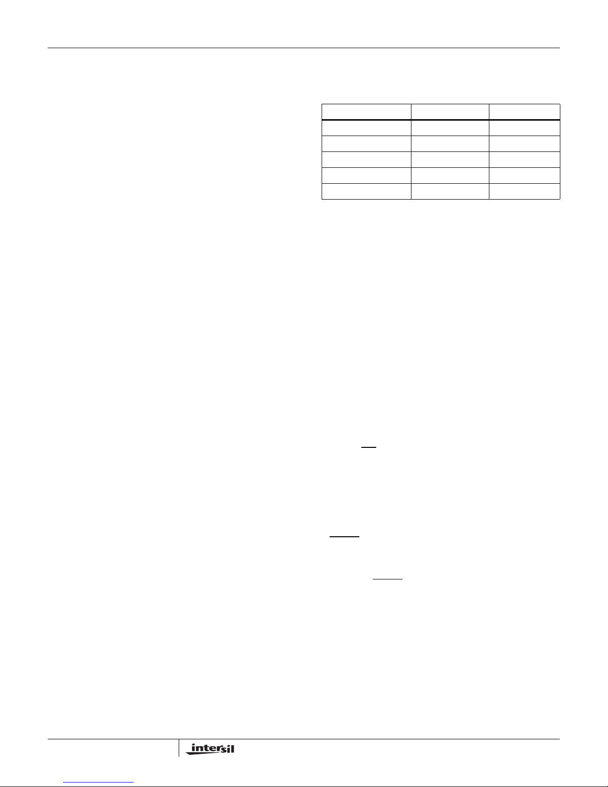
“DZ/(SLEW)” (13) and “SPB” (9) jumpers for the desired Tx
speed setting. Table 1 details the jumper settings for each of
the speed options.
,
3
AN1248.1
May 30, 2006
Page 4
Application Note 1248
TABLE 1. JUMPER SETTINGS FOR Tx SPEED SELECTION
DATA RATE J-(DZ/SLEW)
(13) J-SPB (9)
115kbps “LOW” “LOW”
460kbps “LOW” “VH”
20Mbps “VH” “LOW” or “VH”
Driver Tests
There are no driver loads on this board, so if loading is
desired a differential load resistor, and/or differential load
capacitor may be added at position “R7”. Alternatively, single
ended loads (Y or Z to GND) may be added at positions “C4”
and “C2”.
Ensure that the “DZ1/DE1 (DY)” (14) jumper is in the “LOW”
position to engage the 50Ω term resistor, connect the
generator to the “DZ1/DE1 (DY)” BNC, and set the swing for
0 to 3V. Monitoring test points “TP18” (input), and “TP5” and
“TP2” (Y and Z outputs respectively) with a scope allows the
Tx prop delays, skews, and transition times to be measured.
To view the differential waveform, use the scope’s math
function to generate “Z-Y”.
To measure the Tx output enable and disable times, start
with the previous jumper configuration and move the
“DEN” (8) jumper to the “LOW” position to engage its 50Ω
term resistor. Connect the generator to the “NC (DEN)” BNC,
and set the swing for 0 to 3V. Monitoring test points “TP9”
(input), and “TP5” and “TP2” (Y and Z outputs respectively)
with a scope allows the enable and disable times to be
measured. Note that some form of termination resistor must
be used to pull the disabled outputs to a known state; a
differential termination resistor at “R7” is the easiest
approach.
Evaluating Driver and Receiver Combined Performance
Performance through a cascaded Tx and Rx can easily be
evaluated, utilizing the external loopback function, by
installing jumpers “A1/Y1_LB (5) and “B1/Z1_LB (6). In this
configuration, the Tx output lines connect to the
corresponding Rx input lines, so the data driven on the Tx
input (DY) appears at the Rx output (RA).
Installing resistors R7 and R9 allows evaluation of the
performance with the Tx driving a double terminated load.
Interconnecting Driver and Receiver with a Cable
To evaluate the performance of the Tx and Rx
interconnected by a cable, start with the default
configuration, connect single wire of a twisted pair between
test points “TP2” and “TP1”, and connect the other wire in
the pair between “TP5” and “TP6”. Ensure that the
“DZ1/DE1 (DY)” (14) jumper is in the “LOW” position to
engage the 50Ω term resistor, connect the generator to the
“DZ1/DE1 (DY)” BNC, and set the swing for 0 to 3V.
Monitoring test points “TP18” (input), and test point
“RB1(RA)” illustrates the overall input to output performance.
Installing resistors R7 and R9 allows evaluation of the
performance with the Tx driving a double terminated cable.
Switching to RS-232 Mode
To set the board for RS-232 evaluation, start with the
jumpers in the “default configuration”, and move jumper
“A2 (485/232
)” (7) to the “LOW” position. If RS-485
termination resistors (“R7” or “R9”) were added, ensure that
they have been removed. Note that the RS-232 data rate is
fixed at 500kbps, so the “SPB” (9) jumper has no affect
(connect it high to minimize SHDN I
), and that the
CC
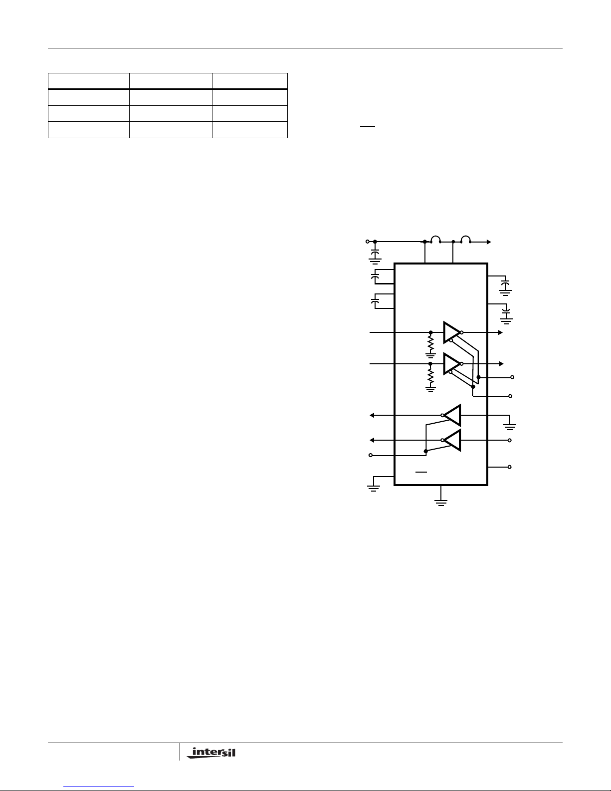
“SLEW” pin becomes the second driver input, DZ. Figure 1
illustrates the 41387 configuration in this mode.
5kΩ
5kΩ
(16)
34
V
CC
GND
+5V
C
0.1μF
C
0.1μF
A1
B1
Y1
Z1
V
+
0.1μF
37
1
2
H
C1+
+
38
C1-
36
C2+
+
35
C2-
2
329
4
5
12
DEN
11
485 / 232
FIGURE 1. DEFAULT RS-232 CONFIGURATION
V
L
R
R
D
D
15, 16
31
(17)
RXEN
ON
V+
V-
D
Y
D
Z
VHIGH (VH )
1
C
+
0.1μF
19
C
0.1μF
+
30
R
A
R
B
20
RXEN
17
V
28
27
V
21
V
3
4
V
H
H
H
H
Basic RS-232 DC Evaluation
General Observations
Note that V+ and V- now pump up to approximately +6V and
-7V, respectively, and the charge pump operation increases
I
to 3.8mA. Also note that RS-232 drivers and receivers
CC
are inverting by definition.
Before starting, ensure that resistors R7 and R9 are
removed, if they have been previously installed.
Receiver Tests
In the default configuration of Figure 1, RB (measure at the
“RA1 (RB)” test point to the left of jumper (14)) and RA
(measure at the “RB1(RA)” test point to the right of
4
AN1248.1
May 30, 2006
Page 5

Application Note 1248
jumper (1)) are high due to the A1 and B1 5kΩ input
resistors to GND.
To switch the Rx output states, install the A1 and B1 Rx bias
jumpers, “J10” (2) and “J9” (3). The “RXBIAS-VCC” (15)
jumper now drives the Rx input voltages to V
CC
, which
switches RA and RB low. Removing the “RXBIAS-VCC”
jumper and connecting a power supply between the
“RXBIAS” banana jack and GND, allows this supply to set
the Rx input voltages, in case the user wants to evaluate the
Rx switching points.
To disable the Rx outputs via the active high RXEN pin,
remove “J10” (2) and “J9” (3), and switch the “(RXEN)” (11)
jumper to the “LOW” position (make sure the “RXEN1
” (10)
jumper is in the “VH” position). To disable the Rx outputs via
the active low RXEN1
pin, move jumper “RXEN1” to the
“VH” position (make sure the “(RXEN)” jumper is in the
“LOW” position).
Return the “RXEN1
” and “(RXEN)” jumpers to the “VH”
position, remove the “RXBIAS” power supply, and reinstall
the “RXBIAS-VCC” (15) jumper.
Driver Tests
The RS-232 Tx outputs, Y and Z, are high (≈6.5V) and low
(≈ -7V), respectively, in the default configuration. To switch
the output states, simply switch the “DY1 (DZ/SLEW)” (13)
and “DZ1/DE1 (DY)” (14) jumpers (note Rev. A label errors)
to the opposite states. To evaluate the loaded driver output
voltages, configure the port for “external loopback”, as
described previously (i.e., install jumpers (5) and (6)). Each
driver output is now loaded by an Rx input resistor (≈5kΩ),
and the output voltages still exceed ±6.2V.
The driver outputs can be disabled by moving the
“(DEN)” (8) jumper to the “LOW” position.
Remove the “external loopback” jumpers when finished,
switch the “DY1(DZ/SLEW)” and “(DEN)” jumpers to the
“VH” position, and move the “DZ1/DE1 (DY)” jumper back to
the “LOW” position.
Internal Loopback
To configure the ISL41387 for internal loopback mode,
simply move the “(ON)” (12) jumper to the “LOW” position,
while ensuring that the “(DEN)” (8) and “(RXEN)” (11)
jumpers are set to “VH”. Note that I
increases due to the
CC
enabling of the loopback receivers. RA is now low due to Tx
output Y feeding back to Rx A, while RB is high due to Z
feeding back to Rx B. You can repeat the previous Rx
switching tests to confirm th at the exter nal Rx input p ins now
have no affect on RA nor RB.
Low Power SHDN
The ISLX1387 enter the SHDN mode when
“(ON)” (12) = “LOW”, and the Tx and Rx are disabled
(“(DEN)” (8) = “LOW”, “(RXEN)” (11) = “LOW”, and
“RXEN1
(10) = “VH”), and the already low supply current
drops to as low as 5µA. SHDN disables the Tx and Rx
outputs, and disables the charge pumps, so V+ collapses to
V
, and V- collapses to GND.
CC
All but 5µA of SHDN ICC current is due to the on-chip SPB
pull-up resistor (~20µA/resistor), so SHDN I
CC
varies
depending on the ISLX1387 configuration. To evaluate the
lowest SHDN I
, ensure that the “SPB” (9) jumper is in the
CC
“VH” position.
Single Tx and Single Transceiver Modes
RS-232 mode also offers the options of selecting a single Tx
mode, or a single Tx/Rx pair mode. T o evaluate the single Tx
mode, set the “(ON)” (12) and “(RXEN)” (11) jumpers “LOW”
and “(DEN)” (8) and “RXEN1
” (10) jumpers to “VH”. To
evaluate the single Tx/Rx mode, set the “(ON)” and “(DEN)”
jumpers “LOW” and either the “RXEN1
” jumper to “LOW” or
the “(RXEN)” jumper to “VH”.
Basic AC Evaluation
Before starting, ensure that the jumpers are back in the
default RS-232 positions. Note that the RS-232 data rate is
fixed, so the speed select pins have no effect.
Receiver Tests
Add jumper “A1” (1) to engage the 50Ω term, connect a
generator to the “A1” BNC, and set it for at least a 0V to 3V
swing. Monitoring test points “TP6” (input), and “RB1(RA)”
(output) with a scope allows the Rx prop delays and skews
to be measured. If desired, you can load the Rx output with a
1kΩ resistor by adding jumper “J6” (not numbered), located
below test point “RB1 (RA)”. This resistor terminates to the
“VLOAD” banana jack (upper left hand corner), allowing the
resistor to be terminated to GND by shorting “VLOAD” to
GND, or terminated to any voltage by connecting “VLOAD”
to an external supply.
To measure the Rx enable/disable time to/from a high output
state via the active high RXEN pin, start from the previous
jumper configuration, leave the “J6” jumper installed, and
connect the “VLOAD” banana jack to GND. Remove the “A1”
jumper (Rx input is pulled low by its on-chip pull-down),
switch the “(RXEN)” (11) jumper to the low position to
engage the 50Ω term, set the generator to swing from 0V to
3V, and move the generator to the “NC (RXEN)” BNC.
Monitoring test points “TP12” (input), and “RB1 (RA)”
(output) with a scope allows the Rx enable and disable times
to be measured. To evaluate the Rx enable/disable time
to/from a low output state, install the A1 Rx bias jumper,
“J10” (2).
To evaluate the Rx enable/disable times using the active low
RXEN
pin, repeat the previous test but leave the “(RXEN)”
jumper in the “LOW” position, move the “RXEN1
jumper to the “LOW” position to connect the 50Ω term, and
connect the generator to the “RXEN1
” BNC.
” (10)
5
AN1248.1
May 30, 2006
Page 6
Application Note 1248
Driver Tests
Ensure that the “DZ1/DE1 (DY)” (14) jumper is in the “LOW”
position to engage the 50Ω term resistor, connect the
generator to the “DZ1/DE1 (DY)” BNC, and set the swing for
0 to 3V. Monitoring test points “TP18” (input) and “TP5”
(output) with a scope, allows the Tx prop delays, skews, and
transition times to be measured.
To measure the “loaded” driver performance, simply remove
the “J10” (2) jumper, and connect the “A1/Y1_LB” (5) jumper ,
which connects an Rx input, including its 5kΩ pull-down, to
the driver output.
To measure the Tx output enable/disable times to/from a
high output state, start with the previous jumper
configuration and move the “(DEN)” (8) jumper to the “LOW”
position to engage its 50Ω term resistor. Connect the
generator to the “NC (DEN)” BNC, and set the swing for 0 to
3V. Monitoring test points “TP9” (input), and “TP5” (output)
with a scope allows the enable and disable times to be
measured. Note that some form of output termination
resistor must be used to pull the disabled output to a known
state; installing the “A1/Y1_LB” jumper is the easiest
solution.
Evaluating Driver and Receiver Combined Performance
Performance through a cascaded Tx and Rx can easily be
evaluated, utilizing the external loopback function. Insure
that the “A1/Y1_LB (5) jumper is installed, that the
“(DEN)” (8) and “(RXEN)” (11) jumpers are set to the “VH”
position, and that the “DZ1/DE1(DY)” (14) jumper is in the
“LOW” position. Connect the generator to the
“DZ1/DE1(DY)” BNC, and set the swing for 0 to 3V.
Monitoring test points “TP18” (input), and “RB1 (RA)”
(output) with a scope allows evaluation of the total Tx and Rx
performance. In this configuration, the Tx output line
connects to an Rx input line, so the data driven on the Tx
input (DY) appears at the Rx output (RA).
Evaluating the Logic Supply (VL) Function
The ISL41387 includes a VL pin that powers the logic inputs
(Tx inputs and control pins) and Rx outputs, regardless of
protocol selection. These pins interface with “logic” devices
such as UARTs, ASICs, and μcontrollers, and today most of
these devices use power supplies significantly lower than
5V. Connecting the V
device limits the ISL41387’s Rx output V
reduces the Tx and control input switching points to values
compatible with the logic device’s output levels. If the logic
device is also powered by 5V, then the V
shorted to the V
Removing jumper “V
power supply to the “V
evaluate this function. V
to 1.65V, but the input switching points may not provide
enough noise margin when V
typical V
and VIL values for various VL settings so the user
IH
pin to the power supply of the logic
L
OH
pin should be
L
CC
pin.
” (16), and connecting a new
CC-VL
” banana jack allows the user to
L
can be anywhere from VCC down
L
< 1.8V. Table 2 indicates
L
to VL, and
can ascertain whether or not a particular V
voltage meets
L
his needs.
TABLE 2. VIH AND VIL vs VL FOR VCC = 5V
(V) VIH (V) VIL (V)
V
L
1.65 0.79 0.50
1.8 0.82 0.60
2.0 0.87 0.69
2.5 0.99 0.86
3.3 1.19 1.05
To evaluate the V
while monitoring a high Rx output. To evaluate the V
impact on Rx VOH, vary the VL voltage
L
effect
L
on input switching points, remove the “VL-VHIGH” (17)
jumper, connect a new supply between the “VHIGH” and
“GND” banana jacks, set the V
supply to the desired
L
voltage, move the jumper of the input to be tested to the
“VH” position, and vary the “VHIGH” supply to determine the
switching point.
Jumper Definitions
The jumpers used to evaluate the ISL41387 are:
J-A1 (1) - Connects A1 input to GND through a 50Ω resistor.
J10 (2) - Connects A1 input to the RXBIAS jack.
J9 (3) - Connects B1 input to the RXBIAS jack.
J-B1 (4) - Connects B1 input to GND through a 50Ω resistor.
A1/Y1_LB (5) - Loops output Y1 back to input A1.
B1/Z1_LB (6) - Loops output Z1 back to input B1.
J-A2(485/232) (7) - “LOW” sets the IC to RS-232 mode;
“VH” sets it to RS-485 mode.
J-(DEN) (8) - “LOW” disables RS-232 or RS-485 Tx outputs;
“VH” enables all Tx outputs.
J-SPB (9) - Used with “SLEW” to set the RS-485 Tx data
rate (see Table 1).
J-RXEN1
outputs; “VH” disables Rx outputs (iff J-(RXEN) = “LOW”).
J-(RXEN) (11) - “LOW” disables all RS-232 or RS-485 Rx
outputs (iff J-RXEN1
J-(ON) (12) - “LOW” places IC in “special features” mode
(loopback, SHDN, etc.); “VH” sets IC for normal operation.
J-DY1(DZ/SLEW) (13) - “LOW” sets the Z Tx input low in
RS-232 mode or selects the slew rate limited data rates in
RS-485 mode; “VH” sets the Z Tx input high in RS-232 mode
or selects the 20Mbps data rate in RS-485 mode.
J-DZ1/DE1(DY) (14) - “LOW” sets the Y Tx input low in
RS-232 or RS-485 Modes; “VH” sets the Y Tx input high in
either mode.
(10) - “LOW” enables all RS-232 or RS-485 Rx
= “VH”); “VH” enables Rx outputs.
6
AN1248.1
May 30, 2006
Page 7
Application Note 1248
RXBIAS-VCC (15) - Connects VCC to the “RXBIAS” jack; if
driving RXBIAS from a voltage other than V
, remove this
CC
jumper.
VCC-VL (16) - Connects V
from a voltage other than V
to the “VL” jack; if driving VL
CC
, remove this jumper.
CC
VL-VHIGH (17) - Connects VL to the “VHIGH” jack; if driving
VHIGH from a voltage other than V
, remove this jumper.
L
PCB Layout Information
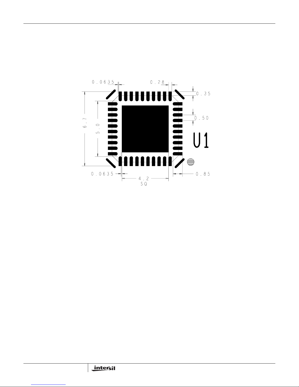
The dimensions for the QFN land pattern used on this board
are shown in Figure 2.
FIGURE 2. QFN LAND PATTERN AND DIMENSIONS (in mm)
7
AN1248.1
May 30, 2006
Page 8
Application Note 1248
15
1
3
2
4
5
6
9
7
8
10
11
14
12
16
17
13
ISL41387EVAL1Z
FIGURE 3. JUMPER LOCATOR DIAGRAM
Intersil Corporation reserves the right to make changes in circuit design, software and/or specifications at any time without notice. Accordingly, the reader is cautioned to
verify that the Application Note or Technical Brief is current before proceeding.
For information regarding Intersil Corporation and its products, see www.intersil.com
8
AN1248.1
May 30, 2006
Page 9
Application Note 1248
B1
TP1
J-B1
J9
A1
R1
Y1
TP5
C4
TP2
Z1
C2
VLOAD
J1
C1
R5
VHIGH
B1/Z1_LB
R6
J-SEL1
R10
VHIGH
J-SEL2
VLOAD
R11
*B2/Z2_LB
J4
C6
TP7
Z2 (NC)
C5
Y2 (NC)
TP3
C3
B2 (NC)
TP8
R4
* Labels swapped on Rev A board
RXBIAS
R9
R7
R13
RXBIAS
J11
VHIGH
R15
J-B2
TP6
1
A1/Y1_LB
2
3
4
5
6
7
8
9
10
R14
*A2/Y2_LB
RXBIAS
J12
J-A2 (485/232
VHIGH
R20
RXBIAS
R3
V+
J10
J-A1
VLOAD
RXBIAS
VLOAD
C26
C27
RXBIAS
C24
C25
C15
P-VCC
GND
VCC
C9
RXBIAS-VCC
C7
C8 C11
C10
VCC-VL
40
39 38 37 36 35 34 33 32 31
NC NC NCC1- C1+ C2+ C2- V
NC V
CC
V+
GND
GND V-
11 12 13 14 15 16 17 18 19 20
VHIGH
J-SPB
VHIGH
J-SPA (NC)
V-
VHIGH
J-RXEN1
TP4
A2 (485/232)
)
@
(to pin 27)
J-(SLEW)
TP20
DY1 (DZ/SLEW)
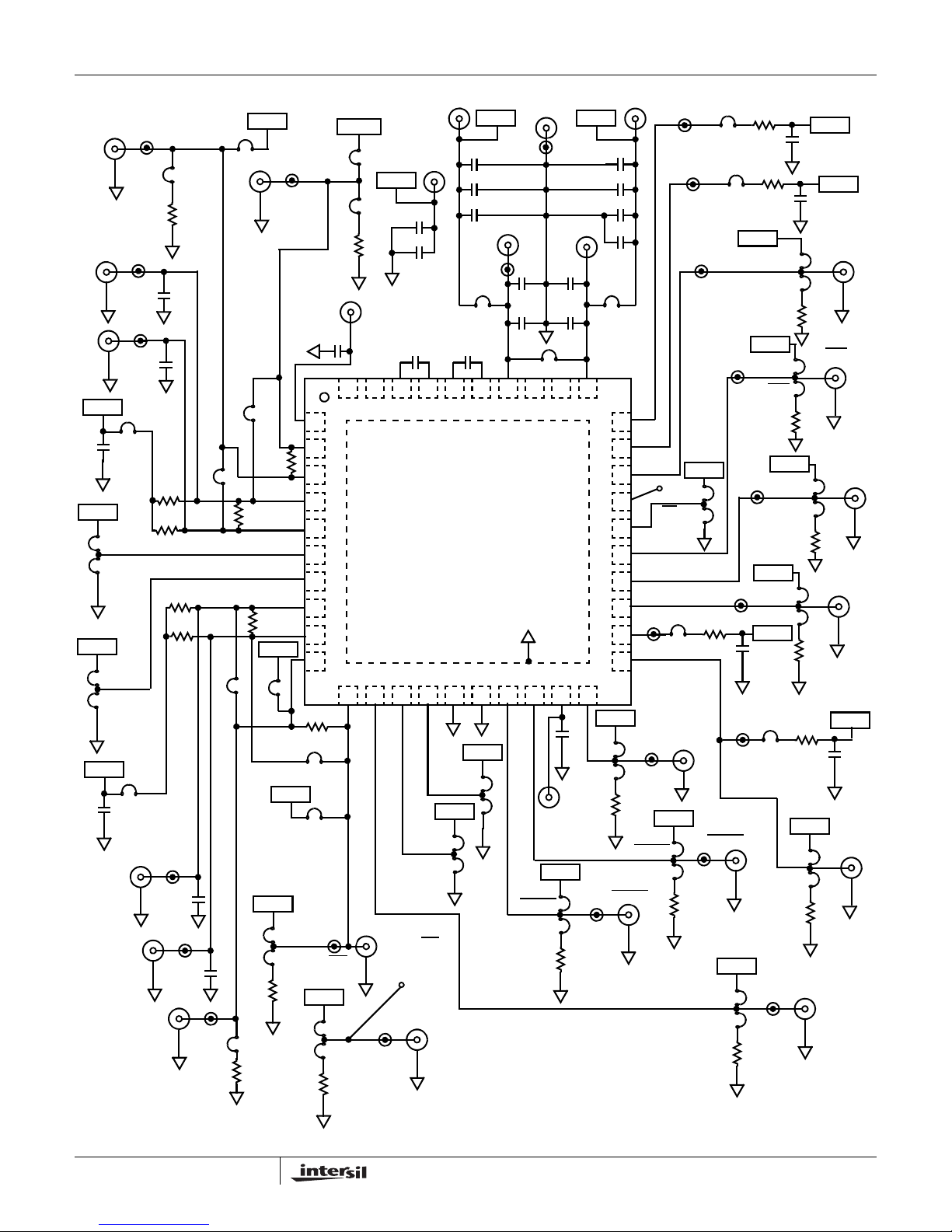
R1, 3, 4, 8, 12, 15-18, 20, 24-26, 28 = 49.9Ω
R5, 6, 10, 11 = 499Ω (NOT POPULATED)
R7, 9 = 121Ω (NOT POPULATED)
R13, 14 = 121Ω
R19, 22, 23, 27 = 1kΩ
C1, 6-8,10-14, 16, 18-21, 23-26 = 0.1μF
C2-5 = 0.1μF (NOT POPULATED)
C9, 15, 17, 22, 27 = 10μF
P-GND
VL
C22
C13
C12
J-RXEN
R16
VHIGH
VL-VHIGH
L
VHIGH
TP11
VHIGH
C14
C23
C16
C17
30
29
28
27
26
25
24
23
22
21
R18
J-RXEN2
RXEN1
RB1(RA)
@
J-LB (NC)
RA2(NC)
NC (RXEN)
TP12
VHIGH
RA1(RB)
TP18
VHIGH
J14
TP10
R17
J-(DEN)
J6
J13
VHIGH
TP16
J-ON/OFF
TP19
TP21
R23
C20
TP17
RXEN2 (NC)
VHIGH
R12
R19
R22
J-DE1
VHIGH
VHIGH
VHIGH
J-DE2
VLOAD
J5
J-(ON)
TP9
C18
C19
ON/OFF (NC)
R25
J-DY2
DZ2/DE2 (NC)
R28
R27
VHIGH
VLOAD
VLOAD
R24
DY2 (NC)
R8
VLOAD
C21
RB2 (ON)
R26
NC (DEN)
DZ1/DE1 (DY)
9
AN1248.1
May 30, 2006
 Loading...