

Page 1
®
ISL28470EVAL1Z Evaluation
Board User’s Guide
Application Note February 12, 2007
Introduction
The ISL28470EVAL1Z evaluation board is a design platform
containing all the circuitry needed to characterize critical
performance parameters of the ISL28470 Quad
Instrumentation Amplifier using a variety of user defined test
circuits.
The ISL28470 is a quad channel instrumentation amplifier
optimized for 2.4V to 5V single supplies. The device features
an Input Range Enhancement Circuit (IREC) which
maintains CMRR performance for input voltages equal to the
positive supply and down to 50mV above the negative
supply rail. The input signal is capable of swinging above the
positive supply rail and to the negative supply with only a
slight degradation of the CMRR performance. The output
operation is rail to rail. The ISL28270 is compensated for a
minimum gain of 100.
Reference Documents
• ISL28470 Data Sheet, FN6260
Evaluation Board Key Features
The ISL28470EVAL1Z is designed to be operated from a
single supply (+2.4VDC to +5VDC), or from split supplies
(±1.2VDC to ±2/5V). The board is configured for 4
independent instrumentation amplifiers connected for a
closed loop gain of 101 with inverting and non-inverting high
impedance terminated with 100k resistors to ground. Each
amplifier contains it’s own VREF input to establish an input
common mode reference. An ENABLE
provided for each amplifier to be used to save power by
powering the device down.
select switch is
AN1289.0
GND V-V+
VP
J
3
V+
R
C
2
++
11
0
4
22
R
D
2
C
9
11
0.1µF 0.1µF
J
2
R
2
22
1
004.7µF 4.7µF
C
D
1
C
10
J
1
V-
1
R
0
3
VM
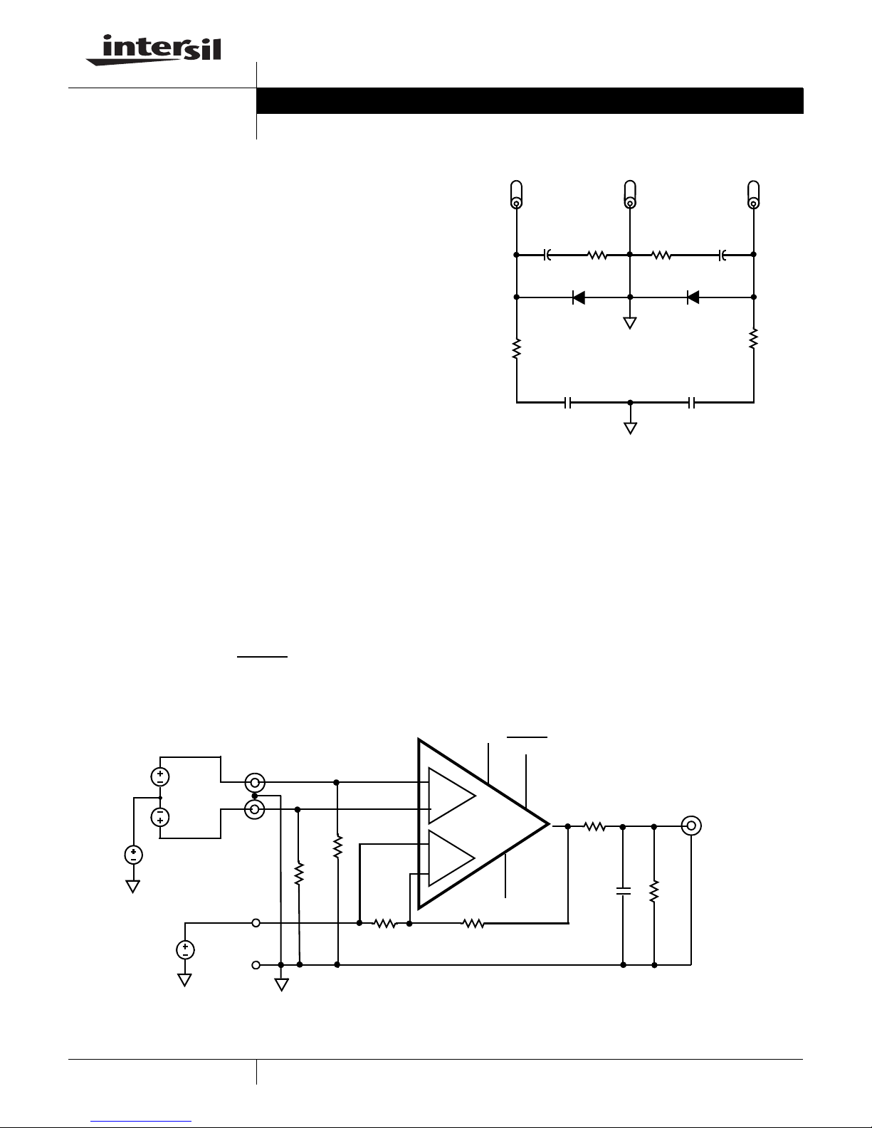
FIGURE 1. POWER SUPPLY CIRCUIT
Power Supplies (Refer to Figure 1)
External power connections are made through the +V, -V
and Ground connections on the evaluation board. For single
supply operation, the -V and Ground pins are tied together to
the power supply negative terminal. For split supplies, +V
and -V terminals connect to their respective power supply
terminals. De-coupling capacitors, C
ground through R
R
are 0Ω but can be changed by the user to provide power
4
and R2, 0Ω resistors. Resistors R3 and
1
supply filtering, or to reduce the voltage rate-of-rise to less
than ±1V/µs. Anti-reverse diodes D
circuit in the case of accidental polarity reversal.
and C2, connect to
1
and D2 protect the
1
IN+(x)
IN+
IN-
IN-(x)
VCM
VREF(x)
VREF
GND
1
VP
ENABLE
IN+
+
IN-
-
100kΩ
100kΩ
R
1kΩ
FB+
+
FB-
-
G
R
F
100kΩ
-V
VM
FIGURE 2. BASIC AMPLIFIER CONFIGURATION
CAUTION: These devices are sensitive to electrostatic discharge; follow proper IC Handling Procedures.
1-888-INTERSIL or 1-888-468-3774
| Intersil (and design) is a registered trademark of Intersil Americas Inc.
All other trademarks mentioned are the property of their respective owners.
1/4 ISL28470
0Ω
10kΩ
Copyright Intersil Americas Inc. 2007. All Rights Reserved
VOUT(x)
Page 2
Application Note 1289
Amplifier Configuration (Figure 2)
The schematic of each of the 4 Op Amps with the
components supplied is shown in Figure 2. The circuit
implements a differential input instrumentation amp with a
closed loop gain of 101. The circuit can operate from a
single 2.4VDC to +5VDC supply, or from dual supplies from
±1.2VDC to ±2.5VDC.The output common mode reference
is applied to the VREF pin, and has a range from ground
(VM) to VP.
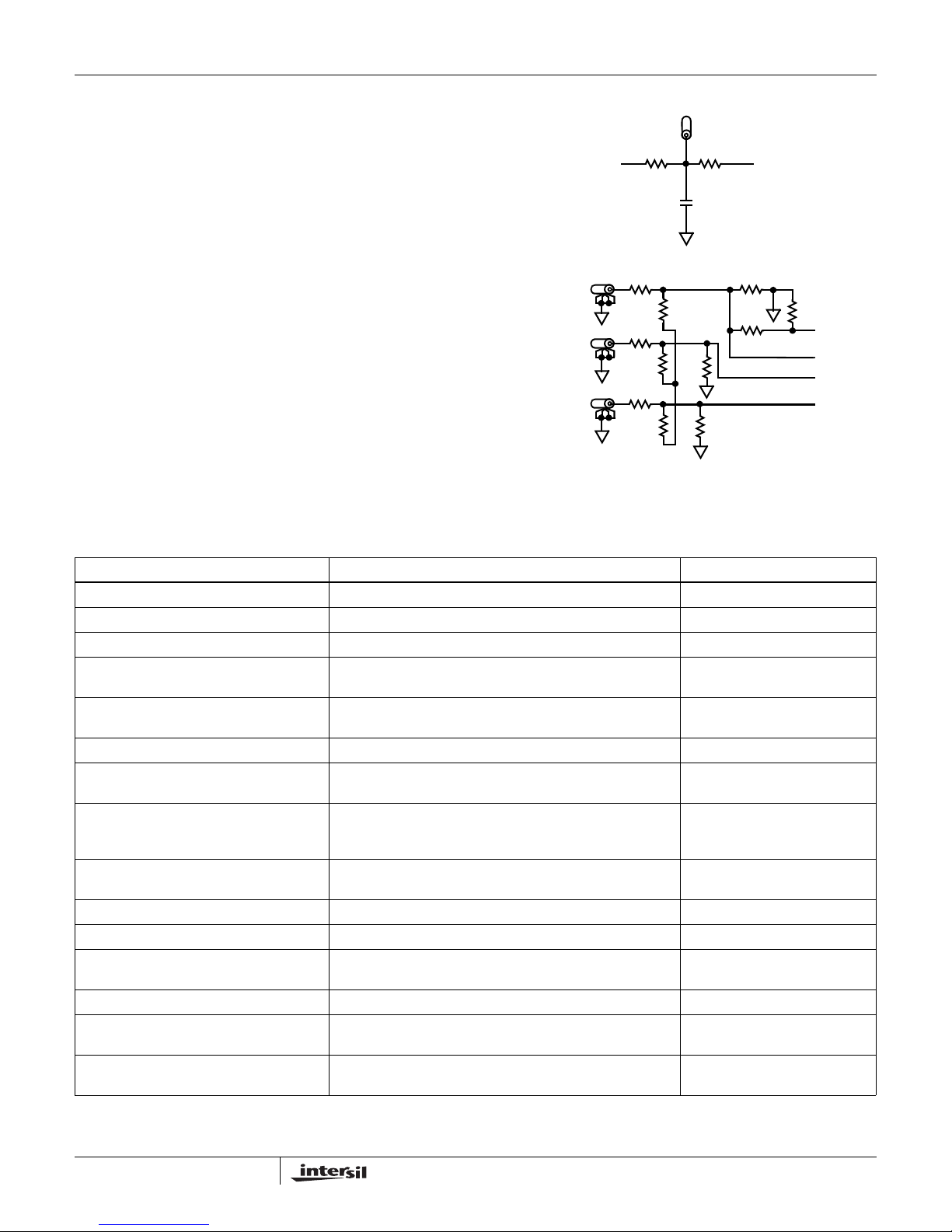
User-selectable Options (Figure 3)
Component pads are included to enable a variety of userselectable circuits to be added to the amplifier differential
inputs, the VREF input, and the amplifier feedback loop. A
voltage divider and filter option can be added to establish a
power supply tracking common mode reference at the VREF
input, or a coaxial connection to the ISL28470 FB+ pin can
be made at the FB+ BNC connector. The differential inputs
have additional resistor placements for adding input
attenuation, or to establish input DC offsets through the
VREF pin.
ISL28470EVAL1Z Components Parts List
VREFA
J
4
1
FB+A
-INA
+INA
R
J
R
8
13
DNP
J
R
9
18
0
R
19
DNP
J
R
10
21
0
R
22
DNP
R
6
C
R
3
14
0
R
100k
DNPDNP
OPEN
VREFA
20
100k
5
VREFA
R
23
V+V-
R
15
DNP
R
17
1k
R
16
DNP
FIGURE 3. COMPONENT-SELECTABLE OPTIONS
DEVICE # DESCRIPTION COMMENTS
C
, C
1
C
, C
7
C9, C
C
3-C6
C
11-C18
D
, D
1
2
8
10
2
CAP-TANTALUM, SMD, D,4.7µF, 50V, 10%, LOW ESR, ROHS Power Supply Decoupling
CAP, SMD, 0603, 0.01µF, 25V, 10%, X7R, ROHS Power Supply Decoupling
CAP, SMD, 0805, 0.1µF, 25V,10%, X7R, ROHS Power Supply Decoupling
CAP, SMD, 0805, DNP-PLACE HOLDER, ROHS Optional VREF Filter
CAP, SMD, 0805, DNP-PLACE HOLDER, ROHS Optional Amplifier Feedback Caps
DIODE-RECTIFIER, SMD, MELF, 2 Ld, 50V, 1A, GPP, ROHS Reverse Power Protection
U1 ISL28470FAZIC INSTRUMENTATION AMP, 28P, QSOP,
ROHS
R
, R14-R16, R19, R22, R24-R27, R30, R33,
13
R
35-R38,R41
R
, R73, R
71
, R21, R29, R32, R40, R43, R51, R54, R58,
R
18
R
, R63, R
60
R
, R28, R39, R
17
R
, R61, R65, R67, R70, R72, R74, R
59
, R23, R31, R34, R42, R45, R53, R56, R57,
R
20
R
, R64, R
62
R
1-R4
R
5-R12
S
1-S4
, R44, R46-R49, R52, R55, R69,
75
66
50
68
76
RESISTOR, SMD, 0603, 0.1%, MF, DNP-PLACE HOLDER User Selectable Resistors
RES, SMD, 0603, 0Ω, 1/16W, TF, ROHS 0Ω User Selectable Resistors
RES, SMD, 0603, 1k, 1/10W, 1%, TF, ROHS RG Gain Resistors
RES, SMD, 0603, 10k, 1/10W, 1%, TF, ROHS
RES, SMD, 0603, 100k, 1/10W, 1%, TF, ROHS RF Gain Resistors
RES, SMD, 0805, 0Ω, 1/8W, TF, ROHS 0Ω User Selectable Resistors
RES, SMD, 0805, DNP-PLACE HOLDER, ROHS User Selectable Resistors
SWITCH-SEALED MINI TOGGLE, TH, 3P, SP, ON/NONE/ON,
GOLD
Not Populated
Not Populated
Not Populated
Not Populated
Enable/Disable Select Switches
2
AN1289.0
February 12, 2007
Page 3
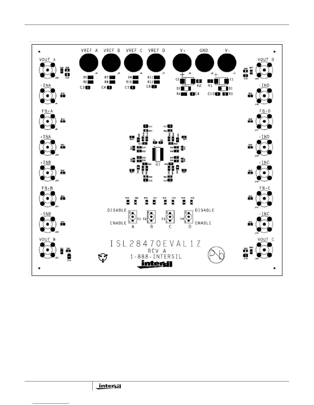
ISL28470EVAL1Z Top View
Application Note 1289
3
AN1289.0
February 12, 2007
Page 4
1
E
Application Note 1289
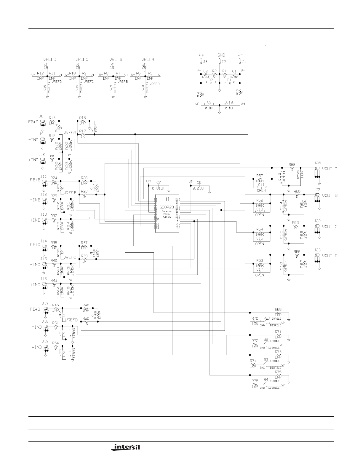
ISL28470EVAL1Z Schematic Diagram
VREFAVREFD VREFC VREFB
V-
FB+A
-INA
+INA
FB+B
-INB
+INB
FB+C
-INC
+INC
FB+D
-IND
+IND
R12
DNP
J8
J9
J10
J11
J12
J13
J14
J15
J16
J7
R11
V+ V- V+ V- V+ V-
DNP
C6
OPEN
R13
DNP
R14
R18
0
R19
R21
0
R22
R24
DNP
R25
R29
0
R30
R32
0
R33
R35
DNP
R36
R40
0
R41
R43
0
R44
J17
R46
DNP
J18
R51
0
J19
R54
0
R10
DNP
0
VREFA
R20
DNP
DNP
R23
0
VREFB
R31
DNP
DNP
R34
0
VREFC
DNP
R42
R45
DNP
0
R47
VREFD
R52
DNP
DNP
R55
100K 100K
100K
100K
100K
100K
R53
R56
J6
C5
R15
DNP
R17
100K
100K
R9
DNP
OPEN
1K
R26
DNP
R28
1K
R37
DNP
R39
1K
R48
DNP
R50
1K
R16
R27
R38
DNP
DNP
DNP
R49
J5
R8
DNPR7DNP
C4
DNP
VREFBVREFCVREFD
OPEN
R6
J4
C3
1
VP
R5
DNPDNP
OPEN
V+
VREFA
C7
0.01UF
1
2
3
4
5
6
7
8
9
10
11
12
13
14
U1
SSOP28
Generic
Pack.
M28.15
DAT
VOUT A
VOUT B
VOUT C
OPEN
1
OPEN
2
OPEN
R58
0
R63
R59
R60
0
0
DESCRIPTION
J20
10K
10K
R61
J22
10K
R65
J21
LTR
ZONE
V+
R4
VP VM
VM
C8
0.01UF
28
27
26
25
24
23
22
21
20
19
18
17
16
15
GND
J2J3
R1
R2
C2
00
D2
1
0
C9
2
0.1UF 0.1UF
D1
1VP2
C10
1
2
V-
J1
V-V+
C1
4.7UF4.7UF
2
0
R3
1
R57
100K
C11
1
OPEN
R62
100K
C13
1
OPEN
R64
100K
C15
2
1
C12
2
2
C14
C16
OPEN
R68
100K
C17
C18
R66
0
OPEN
R67
J23
VOUT D
10K
OPEN
R69
DNP
S1
3
2
ENA
ENABLE
1
DISABLE
VP
R70
10K
R71
DNP
S2
ENB
ENC
END
DISABLE
S3
S4
DISABLE
ENABLE
R73
DNP
ENABLE
DISABLE
R75
DNP
ENABLE
VP
TITLE:
VP
ISL28470EVAL1Z
ENGINEER:
ROBERT POSPISIL
REV:
DATE
0
R72
10K
R74
10K
R76
10K
Intersil Corporation reserves the right to make changes in circuit design, software and/or specifications at any time without notice. Accordingly, the reader is cautioned to
verify that the Application Note or Technical Brief is current before proceeding.
For information regarding Intersil Corporation and its products, see www.intersil.com
4
AN1289.0
February 12, 2007
 Loading...