


®
ICM7555, ICM7556
Data Sheet November 2002
General Purpose Timers
The ICM7555 and ICM7556 are CMOS RC timers providing
significantly improved performance over the standard
SE/NE555/6 and 355 timers, while at the same time being
direct replacements for those devices in most applications.
Improved parameters include low supply current, wide
operating supply voltage range, low THRESHOLD,
TRIGGER
and RESET currents, no crowbarring of the
supply current during output transitions, higher frequency
performance and no requirement to decouple CONTROL
VOLTAGE for stable operation.
Specifically, the ICM7555 and ICM7556 are stable
controllers capable of producing accurate time delays or
frequencies. The ICM7556 is a dual ICM7555, with the two
timers operating independently of each other, sharing only
V+ and GND. In the one shot mode, the pulse width of each
circuit is precisely controlled by one external resistor and
capacitor. For astable operation as an oscillator, the free
running frequency and the duty cycle are both accurately
controlled by two external resistors and one capacitor. Unlike
the regular bipolar 555/6 devices, the CONTROL VOLTAGE
terminal need not be decoupled with a capacitor. The circuits
are triggered and reset on falling (negative) waveforms, and
the output inverter can source or sin k currents large enough
to drive TTL loads, or provi de minima l offsets to dri ve CMOS
loads.
Applications
• Precision Timing
• Pulse Generation
• Sequential Timing
• Time Delay Generation
• Pulse Width Modulation
• Pulse Position Modulation
• Missing Pulse Detector
FN2867.6
Features
• Exact Equivalent in Most Cases for SE/NE555/556 or
TLC555/556
• Low Supply Current
- ICM7555. . . . . . . . . . . . . . . . . . . . . . . . . . . . . . . . 60µA
- ICM7556. . . . . . . . . . . . . . . . . . . . . . . . . . . . . . . 120µA
• Extremely Low Input Currents . . . . . . . . . . . . . . . . . 20pA
• High Speed Operation . . . . . . . . . . . . . . . . . . . . . . . 1MHz
• Guaranteed Supply Voltage Range . . . . . . . . . 2V to 18V
o
• Temperature Stability . . . . . . . . . . . . 0.005%/
C at 25oC
• Normal Reset Function - No Crowbarri ng of Suppl y During
Output Transition
• Can be Used with Higher Impedance Timing Elements
than Regular 555/6 for Longer RC Time Constants
• Timing from Microseconds through Hours
• Operates in Both Astable and Monostable Modes
• Adjustable Duty Cycle
• High Output Source/Sink Driver can Drive TTL/CMOS
• Outputs have Very Low Offsets, HI and LO
Ordering Information
PART NUMBER
ICM7555CBA (7555CBA) 0 to 70 8 Ld SOIC M8.15
ICM7555IBA (7555IBA) -25 to 85 8 Ld SOIC M8.15
ICM7555IPA -25 to 85 8 Ld PDIP E8.3
ICM7556IPD -25 to 85 14 Ld PDIP E14.3
ICM7556MJD -55 to 125 14 Ld CERDIP F14.3
TEMP.
RANGE(oC) PACKAGE PKG. NO.
Pinouts
GND
TRIGGER
OUTPUT
RESET
ICM7555 (PDIP, SOIC)
TOP VIEW
1
2
3
4
8
7
6
5
1
V
DD
DISCHARGE
THRESHOLD
CONTROL
VOLTAGE
ICM7556 (PDIP, CERDIP)
TOP VIEW
DISCHARGE
THRESH-
CONTROL
VOLTAGE
OUTPUT
TRIGGER
CAUTION: These devices are sensitive to electrostatic discharge; follow proper IC Handling Procedures.
1-888-INTERSIL or 321-724-7143
1
2
OLD
3
RESET
4
5
6
GND
7
| Intersil (and design) is a registered trademark of Intersil Americas Inc.
All other trademarks mentioned are the property of their respective owners.
Copyright © Intersil Americas Inc. 2002. All Rights Reserved
14
V
DD
DISCHARGE
13
12
THRESHOLD
CONTROL
11
VOLTAGE
RESET
10
OUTPUT
9
8
TRIGGER
ICM7555, ICM7556
Absolute Maximum Ratings Thermal Information
Supply Voltage. . . . . . . . . . . . . . . . . . . . . . . . . . . . . . . . . . . . . .+18V
Input Voltage
Trigger
, Control Voltage, Threshold,
(Note 1) . . . . . . . . . . . . . . . . . . . . . V+ +0.3V to GND -0.3V
Reset
Output Current. . . . . . . . . . . . . . . . . . . . . . . . . . . . . . . . . . . . 100mA
Thermal Resistance (Typical, Note 2) θ
14 Lead CERDIP Package . . . . . . . . . 80 24
14 Lead PDIP Package. . . . . . . . . . . . 115 N/A
8 Lead PDIP Package. . . . . . . . . . . . . 130 N/A
8 Lead SOIC Package. . . . . . . . . . . . . 170 N/A
Maximum Junction Temperature (Hermetic Package). . . . . . . . 175
Operating Conditions
Temperature Range
ICM7555C . . . . . . . . . . . . . . . . . . . . . . . . . . . . . . . . 0
ICM7555I, ICM7556I . . . . . . . . . . . . . . . . . . . . . . . -25
ICM7556M . . . . . . . . . . . . . . . . . . . . . . . . . . . . . . -55
CAUTION: Stresses above those listed in “Absolute Ma ximum Rat ings” may cause permanen t damage to the devi ce. This is a stress only ra ting and oper ation of th e
device at these or any other conditions above those indicated in the operational sections of this specification is not implied.
o
C to 70oC
o
C to 85oC
o
C to 125oC
Maximum Junction Temperature (Plastic Package) . . . . . . . 150
Maximum Storage Temperature Range . . . . . . . . . -65
Maximum Lead Temperature (Soldering 10s) . . . . . . . . . . . . 300
(SOIC - Lead Tips Only)
NOTES:
1. Due to the SCR structure inherent in the CMOS process used to fabricate these devices, connecting any terminal to a voltage greater than V+
+0.3V or less than V- -0.3V may cause destructive latchup. For this reason it is recommended that no inputs from external sources not operating
from the same power supply be applied to the device before its power supply is established. In multiple supply systems, the supply of the
ICM7555/6 must be turned on first.
is measured with the component mounted on a low effective thermal conductivity test board in free air. See Tech Brief 379 for details.
2. θ
JA
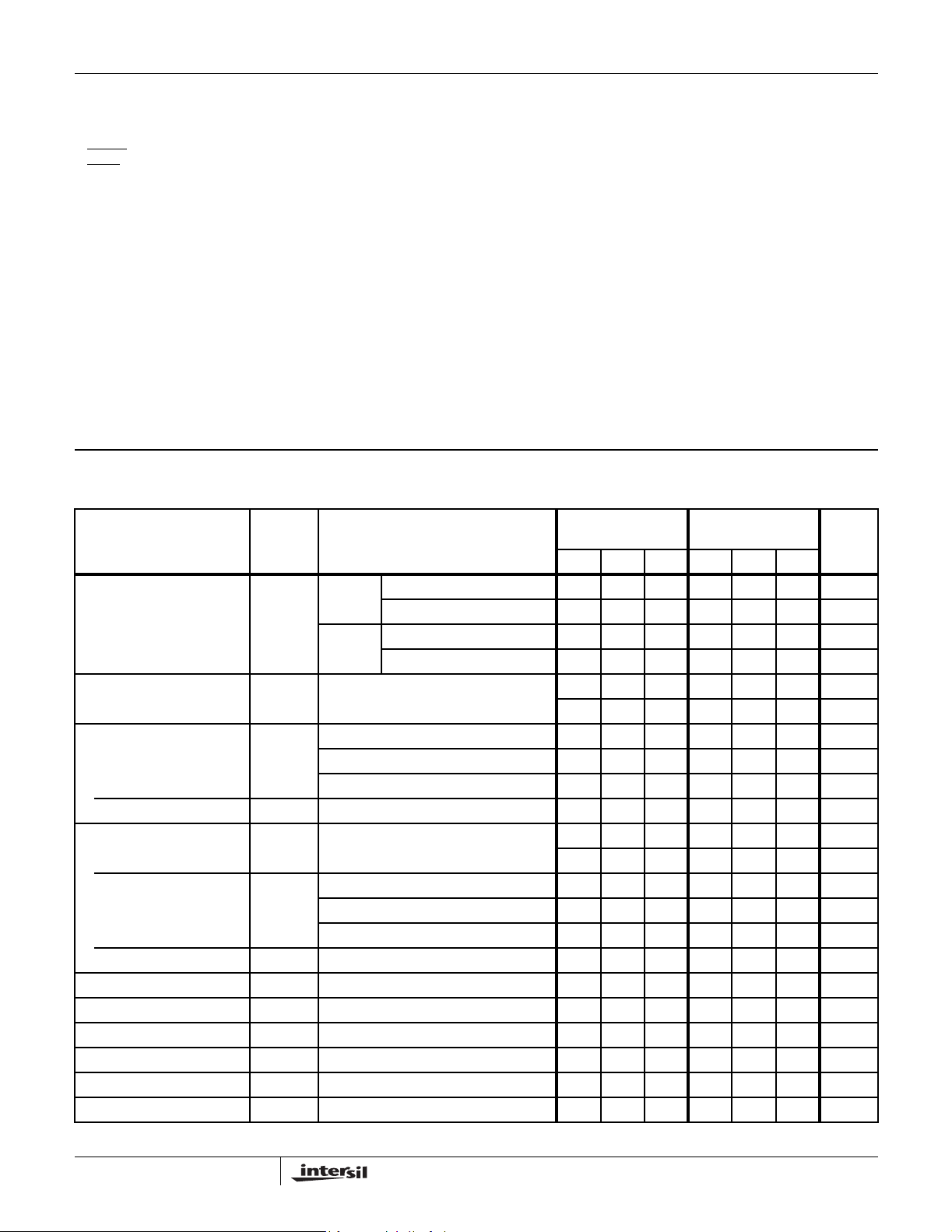
Electrical Specifications Applies to ICM7555 and ICM7556, Unless Otherwise Specified
T
= 25oC
A
PARAMETER SYMBOL TEST CONDITIONS
Static Supply Current I
Monostable Timing Accuracy R
Drift with Temperature
(Note 3)
Drift with Supply (Note 3) V
Astable Timing Accuracy R
Drift with Temperature
(Note 3)
Drift with Supply (Note 3) V
Threshold Voltage V
Trigger Voltage V
Trigger Current I
TRIGVDD
TRIG
Threshold Current I
Control Voltage V
Reset Voltage V
ICM7555 VDD = 5V - 40 200 - - 300 µA
DD
V
= 15V - 60 300 - - 300 µA
DD
ICM7556 V
= 10K, C = 0.1µF, VDD = 5V -2---- %
A
= 5V - 80 400 - - 600 µA
DD
= 15V - 120 600 - - 600 µA
V
DD
- - - 858 - 1161 µs
= 5V - - - - 150 - ppm/oC
V
DD
V
= 10V - - - - 200 - ppm/oC
DD
V
= 15V - - - - 250 - ppm/oC
DD
= 5V to 15V - 0.5 - - 0.5 - %/V
DD
= RB = 10K, C = 0.1µF, VDD = 5V -2---- %
A
- - - 1717 - 2323 µs
= 5V - - - - 150 - ppm/oC
V
DD
= 10V - - - - 200 - ppm/oC
V
DD
V
= 15V - - - - 250 - ppm/oC
DD
= 5V to 15V - 0.5 - - 0.5 - %/V
DD
VDD = 15V 62 67 71 61 - 72 % V
TH
= 15V 28 32 36 27 - 37 % V
VDD = 15V - - 10 - - 50 nA
VDD = 15V - - 10 - - 50 nA
TH
VDD = 15V 62 67 71 61 - 72 % V
CV
VDD = 2V to 15V 0.4 - 1.0 0.2 - 1.2 V
RST
(oC/W) θJC (oC/W)
JA
(NOTE 4)
-55oC TO 125oC
o
C to 150oC
UNITSMIN TYP MAX MIN TYP MAX
o
C
o
C
o
C
DD
DD
DD
2
ICM7555, ICM7556
Electrical Specifications Applies to ICM7555 and ICM7556, Unless Otherwise Specified
T
A
PARAMETER SYMBOL TEST CONDITIONS
Reset Current I
RST
Discharge Leakage I
Output Voltage V
V
Discharge Output Voltage V
Supply Voltage (Note 3) V
Output Rise Time (Note 3) t
Output Fall Time (Note 3) t
Oscillator Frequency
(Note 3)
f
MAX
NOTES:
3. These parameters are based upon characterization data and are not tested.
4. Applies only to military temperature range product (M suffix).
VDD = 15V - - 10 - - 50 nA
VDD = 15V - - 10 - - 50 nA
DIS
VDD = 15V, I
OL
= 5V, I
V
DD
VDD = 15V, I
OH
= 5V, I
V
DD
VDD = 5V, I
DIS
V
= 15V, I
DD
Functional Operation 2.0 - 18.0 3.0 - 16.0 V
DD
RL = 10M, CL = 10pF, VDD = 5V - 75 - - - - ns
R
RL = 10M, CL = 10pF, VDD = 5V - 75 - - - - ns
F
VDD = 5V, RA = 470Ω, RB = 270Ω,
= 20mA - 0.4 1.0 - - 1.25 V
SINK
= 3.2mA - 0.2 0.4 - - 0.5 V
SINK
SOURCE
SOURCE
SINK
SINK
= 0.8mA 14.3 14.6 - 14.2 - - V
= 0.8mA 4.0 4.3 - 3.8 - - V
= 15mA - 0.2 0.4 - - 0.6 V
= 15mA -----0.4 V
-1----MHz
C = 200pF
= 25oC
(NOTE 4)
-55oC TO 125oC
UNITSMIN TYP MAX MIN TYP MAX
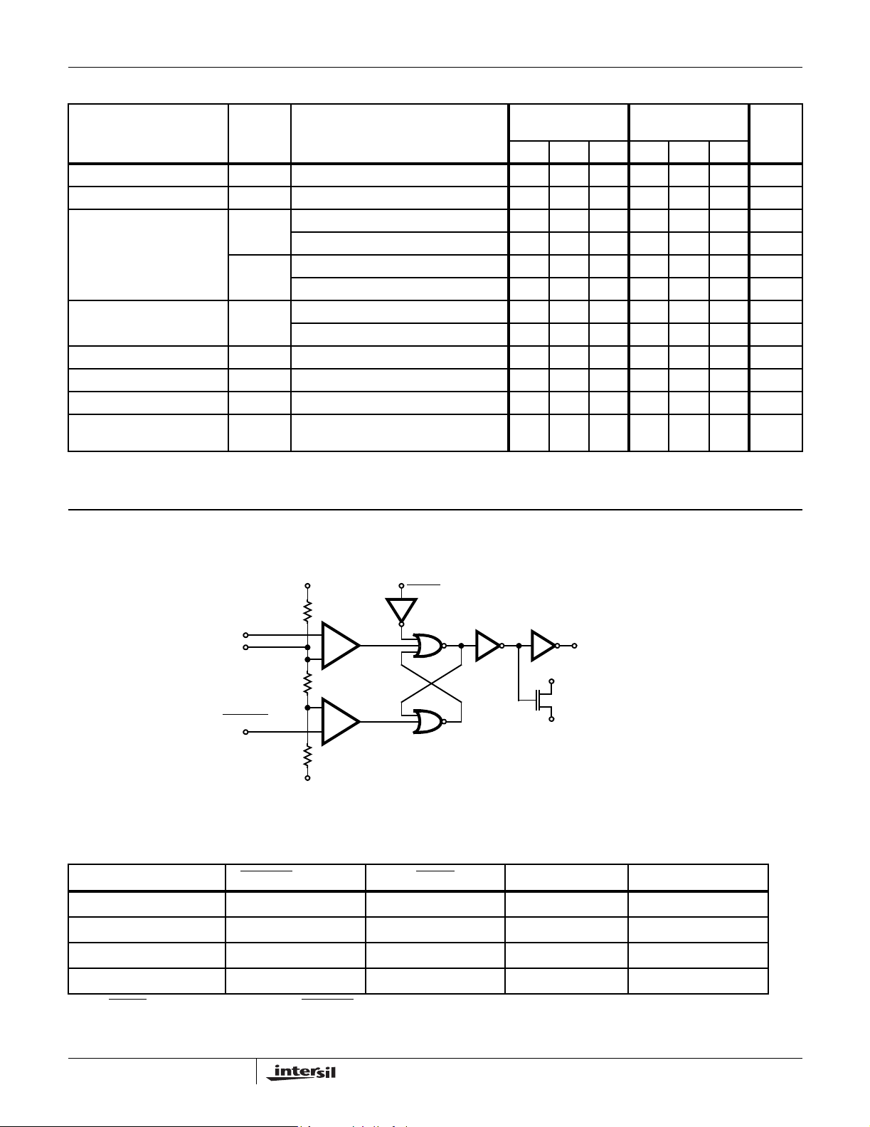
Functional Diagram
V
DD
8
R
COMPARATOR
THRESHOLD
6
5
CONTROL
VOLTAGE
TRIGGER
2
R
R
GND
A
+
-
+
-
COMPARATOR
B
1
NOTE: This functional diagram reduces the circuitry down to its simplest equivalent components. Tie down unused inputs.
THRESHOLD VOLTAGE TRIGGER
VOLTAGE RESET OUTPUT DISCHARGE SWITCH
Don’t Care Don’t Care Low Low On
2
>
/3(V+) >1/3(V+) High Low On
2
<
/3(V+) >1/3(V+) High Stable Stable
Don’t Care <
1
/3(V+) High High Off
FLIP-FLOP
4
RESET
TRUTH TABLE
OUTPUT
DRIVERS
3
7
DISCHARGE
n
1
OUTPUT
NOTE: RESET
will dominate all other inputs: TRIGGER will dominate over THRESHOLD.
3
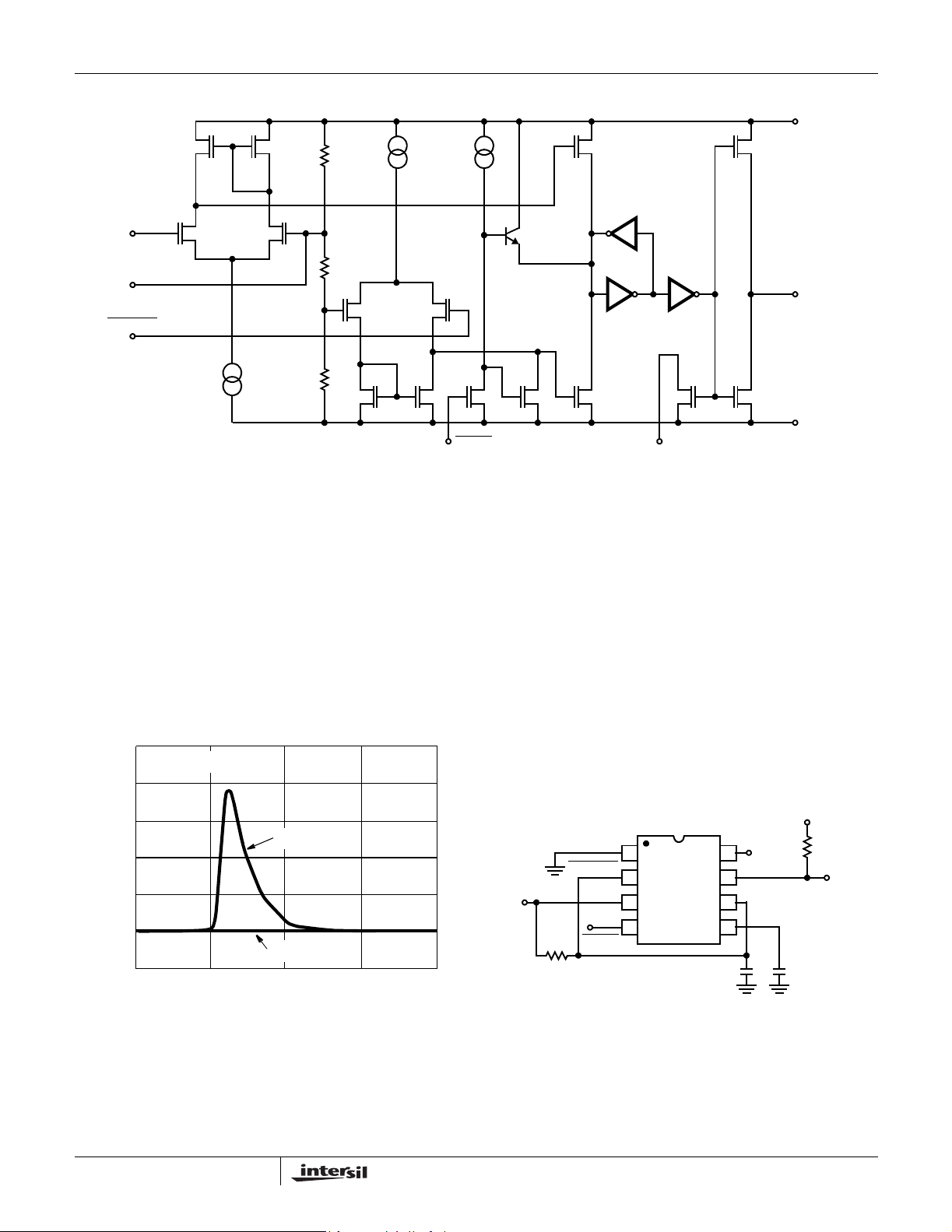
Schematic Diagram
ICM7555, ICM7556
PP P
R
V
P
DD
THRESHOLD
CONTROL
VOLTAGE
TRIGGER
R = 100kΩ ±20% (TYP)
NN
R
R
Application Information
General
The ICM7555/6 devices are, in most instances, direct
replacements for the NE/SE 555/6 devices. However, it is
possible to effect economies in the external component
count using the ICM7555/6. Because the bipolar 555/6
devices produce large crowbar currents in the output driver,
it is necessary to decouple the power supply lines with a
good capacitor close to the device. The 7555/6 devices
produce no such transients. See Figure 1.
500
400
TA = 25oC
NPN
PP
NNNNN
RESET DISCHARGE
The ICM7555/6 produces supply current spikes of only
2mA - 3mA instead of 300mA - 400mA and supply
decoupling is normally not necessary. Also, in most
instances, the CONTROL VOLTAGE decoupling capacitors
are not required since the input impedance of the CMOS
comparators on chip are very high. Thus, for many
applications 2 capacitors can be saved using an ICM7555,
and 3 capacitors with an ICM7556.
POWER SUPPLY CONSIDERATIONS
Although the supply current consumed by the ICM7555/6
devices is very low, the total system supply current can be
high unless the timing components are high impedance.
Therefore, use high values for R and low values for C in
Figures 2 and 3.
OUTPUT
NN
GND
300
SE/NE555
200
100
SUPPLY CURRENT (mA)
0
ICM7555/56
400 8006002000
TIME (ns)
FIGURE 1. SUPPLY CURRENT TRANSIENT COMPARED WITH
A STANDARD BIPOLAR 555 DURING AN OUTPUT
TRANSITION
4
OUTPUT
GND
TRIGGER
R
V
DD
RESET
1
2
3
4
FIGURE 2A. ASTABLE OPERATION
V
DD
8
DISCHARGE
7
THRESHOLD
6
5
C
V
DD
10K
CONTROL
VOLTAGE
OPTIONAL
CAPACITOR
ALTERNATE
OUTPUT