Intersil Corporation ICM7216BLPL, ICM7216DLPL Datasheet
TM
ICM7216B, ICM7216D
Data Sheet February 2002
8-Digit, Multi-Function, Frequency
Counters/Timers
The ICM7216B is a fully integrated Timer Counters with LED
display drivers. They combine a high frequency oscillator, a
decade timebase counter, an 8-decade data counter and
latches, a 7-segment decoder, digit multiplexers and 8segment and 8-digit drivers which directly drive large
multiplexed LED displays. The counter inputs have a
maximum frequency of 10MHz in frequency and unit counter
modes and 2MHz in the other modes. Both inputs are digital
inputs. In many applications, amplification and level shifting
will be required to obtain proper digital signals for these
inputs.
The ICM7216B can function as a frequency counter, period
counter, frequency ratio (fA/fB) counter, time interval counter
or as a totalizing counter. The counter uses either a 10MHz
or 1MHz quartz crystal timebase. For period and time
interval, the 10MHz timebase gives a 0.1
period average and time interval average, the resolution can
be in the nanosecond range. In the frequency mode, the
user can select accumulation times of 0.01s, 0.1s, 1s and
10s. With a 10s accumulation time, the frequency can be
displayed to a resolution of 0.1Hz in the least significant
digit. There is 0.2s between measurements in all ranges.
The ICM7216D functions as a frequency counter only, as
described above.
All versions of the ICM7216 incorporate leading zero
blanking. Frequency is displayed in kHz. In the ICM7216B,
time is displayed in
with a 12.2% duty cycle for each digit. The ICM7216B and
ICM7216D are designed for common cathode displays with
typical peak segment currents of 12mA. In the display off
mode, both digit and segment drivers are turned off,
enabling the display to be used for other functions.
µ
s. The display is multiplexed at 500Hz
µ
s resolution. In
FN3166.3
Features, All Versions
• Functions as a frequency counter (DC to 10MHz)
•Four internal gate times: 0.01s, 0.1s, 1s, 10s in frequency
counter mode
• Directly drives digits and segments of large multiplexed
LED displays (common anode and common cathode
versions)
• Single nominal 5V supply required
• Highly stable oscillator, uses 1MHz or 10MHz crystal
• Internally generated decimal points, interdigit blanking,
leading zero blanking and overflow indication
• Display off mode turns off display and puts chip into low
power mode
• Hold and reset inputs for additional flexibility
Features, ICM7216B
• Functions also as a period counter, unit counter,
frequency ratio counter or time interval counter
•1 cycle, 10 cycles, 100 cycles, 1000 cycles in period,
frequency ratio and time interval modes
µ
• Measures period from 0.5
s to 10s
Features, ICM7216D
• Decimal point and leading zero banking may be externally
selected
Ordering Information
PART
NUMBER
ICM7216BlPl -25
ICM7216DlPl -25
TEMP. RANGE
(oC) PACKAGE PKG. NO.
∞
to 85 28 Ld PDIP E28.6
∞
to 85 28 Ld PDIP E28.6
1
CAUTION: These devices are sensitive to electrostatic discharge; follow proper IC Handling Procedures.
1-888-INTERSIL or 321-724-7143
|
Intersil (and design) is a trademark of Intersil Americas Inc.
Copyright © Intersil Americas Inc. 2002. All Rights Reserved
ICM7216B
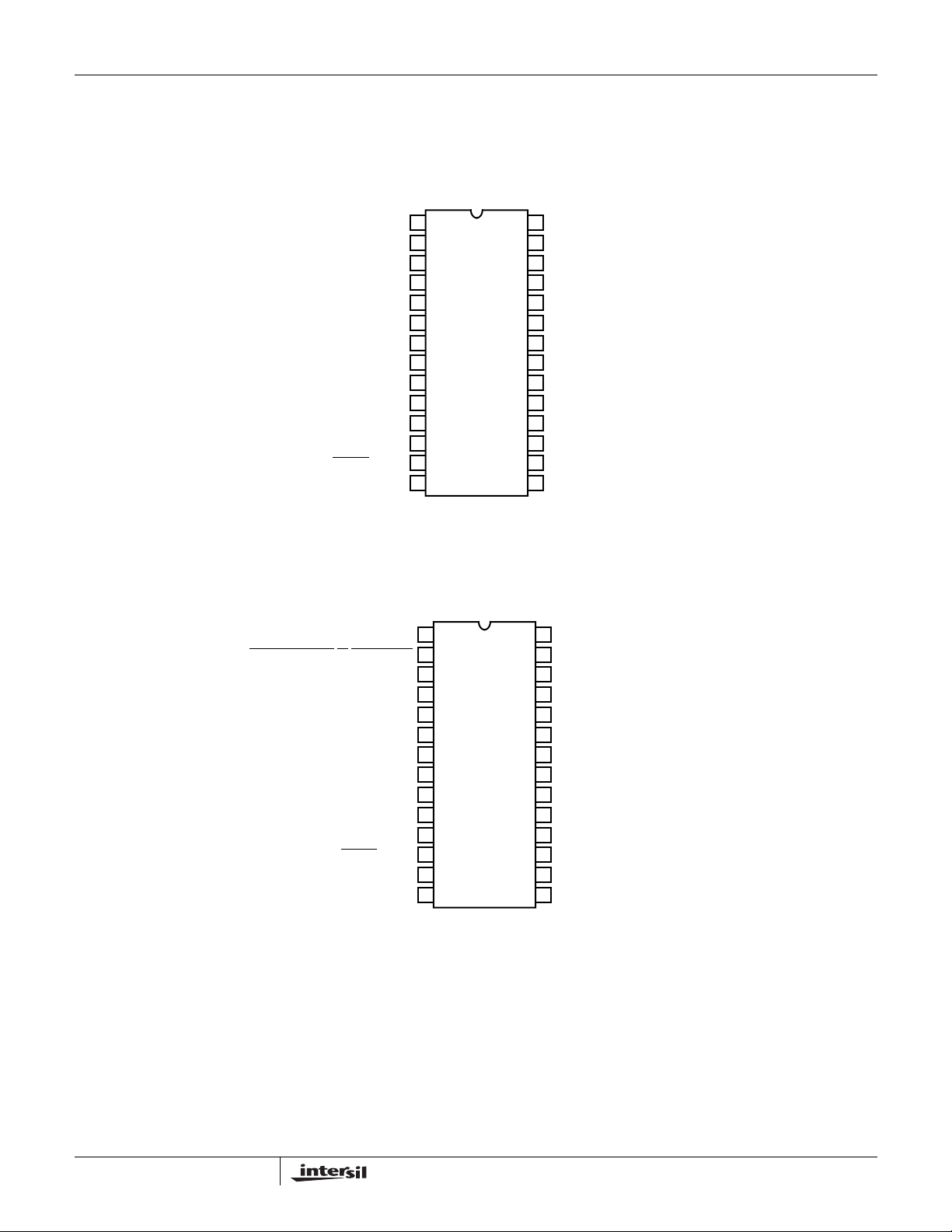
Pinouts
ICM7216B
COMMON CATHODE
(PDIP)
TOP VIEW
28
CONTROL INPUT
INPUT B
FUNCTION INPUT
DIGIT 1 OUTPUT
DIGIT 3 OUTPUT
DIGIT 2 OUTPUT
DIGIT 4 OUTPUT
V
SS
DIGIT 5 OUTPUT
DIGIT 6 OUTPUT
DIGIT 7 OUTPUT
DIGIT 8 OUTPUT
RESET
INPUT
RANGE INPUT
1
2
3
4
5
6
7
8
9
10
11
12
13
14
INPUT A
27
HOLD INPUT
26
OSC OUTPUT
25
OSC INPUT
24
EXT OSC INPUT
23
DECIMAL POINT OUTPUT
g OUTPUT
SEG
22
SEG e OUTPUT
21
20
a OUTPUT
SEG
SEG
d OUTPUT
19
18
V
DD
SEG b OUTPUT
17
16
SEG
c OUTPUT
SEG f OUTPUT
15
CONTROL INPUT
MEASUREMENT
EX. DECIMAL POINT INPUT
IN PROGRESS
DIGIT 1 OUTPUT
DIGIT 3 OUTPUT
DIGIT 2 OUTPUT
DIGIT 4 OUTPUT
DIGIT 5 OUTPUT
DIGIT 6 OUTPUT
DIGIT 7 OUTPUT
DIGIT 8 OUTPUT
RESET
RANGE INPUT
ICM7216D
COMMON CATHODE
TOP VIEW
1
2
3
4
5
6
V
7
SS
8
9
10
11
INPUT
12
13
14
(PDIP)
28
INPUT A
HOLD INPUT
27
26
OSC OUTPUT
25
OSC INPUT
24
EXT OSC INPUT
23
DECIMAL POINT OUTPUT
SEG
g OUTPUT
22
e OUTPUT
21
SEG
20
a OUTPUT
SEG
SEG
d OUTPUT
19
V
18
DD
17
SEG b OUTPUT
16
SEG
c OUTPUT
SEG
f OUTPUT
15
2

F
T
L
Functional Block Diagram
EXT
OSC
INPUT
OSC
INPUT
OSC
OUTPUT
OSC
SELECT
ICM7216B
38 8
REFERENCE
COUNTER
3
10
÷
DECODER
DIGIT
DRIVERS
DIGIT
OUTPUTS
(8)
RESET
INPUT
INPUT A
INPUT B
(NOTE 1)
INPUT
CONTROL
LOGIC
INPUT
CONTROL
LOGIC
100Hz
104 OR ÷10
÷
Q
D
CL
5
EN
CL
4 4444444
DATA LATCHES AND
MAIN
FF
MAIN
103 COUNTER
÷
OUTPUT MUX
RANGE SELECT
LOGIC
STORE AND
RESET LOGIC
OVERFLOW
STORE
RANGE
CONTROL
LOGIC
5
CONTROL
LOGIC
6
DP
LOGIC
DECODER
LOGIC
47 8
SEGMENT
DRIVER
RANGE
INPUT
CONTRO
INPUT
EXT
DP
INPUT
(NOTE 2)
SEGMEN
OUTPUTS
(8)
MEASUREMENT
IN PROGRESS
OUTPUT
(NOTE 2)
UNCTION
INPUT
(NOTE 1)
HOLD
INPUT
FN
CONTROL
LOGIC
6
NOTES:
1. Function input and input B available on ICM7216B only.
2. Ext DP input and MEASUREMENT IN PR
OGRESS output available on ICM7216D only.
3
ICM7216B
Absolute Maximum Ratings Thermal Information
Maximum Supply Voltage (V
Maximum Digit Output Current . . . . . . . . . . . . . . . . . . . . . . . .400mA
Maximum Segment Output Current . . . . . . . . . . . . . . . . . . . . .60mA
Voltage On Any Input or
Output Terminal (Note 1). . . . . . . . . . . (V
DD
- V
). . . . . . . . . . . . . . . . . . .6.5V
SS
+0.3V) to (V
DD
SS
-0.3V)
Thermal Resistance (Typical, Note 4)
PDIP Package . . . . . . . . . . . . . . . . . . . 55 N/A
Maximum Junction Temperature
PDIP Package . . . . . . . . . . . . . . . . . . . . . . . . . . . . . 150
Maximum Storage Temperature Range . . . . . . . . . .-65
Maximum Lead Temperature (Soldering 10s) . . . . . . . . . . . . . 300
o
(
C/W)
θ
JA
Operating Conditions
o
Temperature Range . . . . . . . . . . . . . . . . . . . . . . . . . . -25
CAUTION: Stresses above those listed in “Absolute Maximum Ratings” may cause permanent damage to the device. This is a stress only rating and operation of
the device at these or any other conditions above those indicated in the operational sections of this specification is not implied.
NOTES:
3. The ICM7216 may be triggered into a destructive latchup mode if either input signals are applied before the power supply is applied or if
input or outputs are forced to voltages exceeding V
4.
is measured with the component mounted on an evaluation PC board in free air.
θ
JA
DD
C to 85
to V
o
C
by more than 0.3V.
SS
(
θ
JC
o
C to 150
o
C/W)
o
C
o
C
o
C
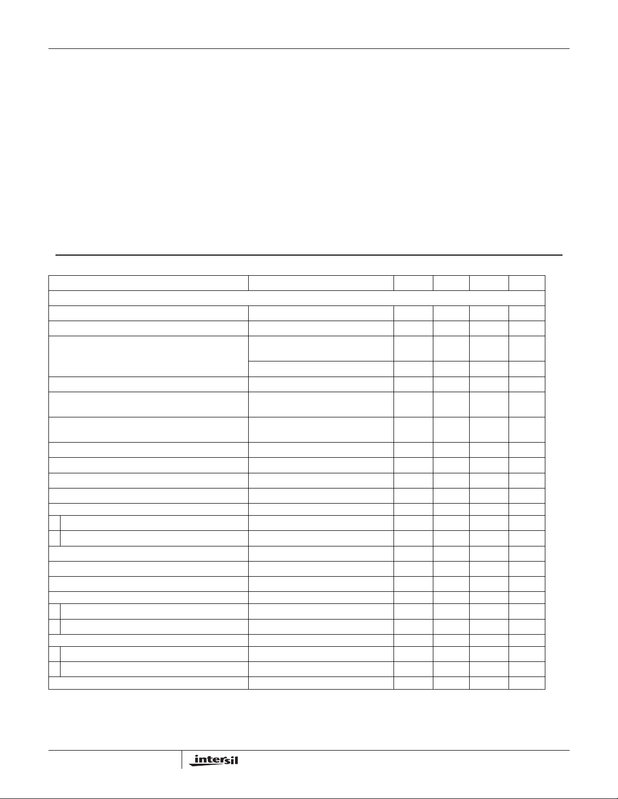
Electrical Specifications
PARAMETER TEST CONDITIONS MIN TYP MAX UNITS
ICM7216B
Operating Supply Current, I
Supply Voltage Range (V
Maximum Frequency INPUT A, Pin 28, f
Maximum Frequency INPUT B, Pin 2, f
Minimum Separation INPUT A to INPUT B Time
Interval Function
Maximum Oscillator Frequency and External Oscillator
Frequency, f
Minimum External Oscillator Frequency, f
Oscillator Transconductance, g
Multiplex Frequency, f
Time Between Measurements f
Input Voltages: Pins 2, 13, 25, 27, 28
Input Low Voltage, V
Input High Voltage, V
Input Resistance to V
Input Leakage Pins 27, 28, 2, I
Input Range of Change, dV
Digit Driver: Pins 4, 5, 6, 7, 9, 10, 11, 12
Low Output Current, I
High Output Current, I
Segment Driver: Pins 15, 16, 17, 19, 20, 21, 22, 23
High Output Current, I
Leakage Current, I
Multiplex Inputs: Pins 1, 3, 14
OSC
DD
MUX
INL
lNH
Pins 13, 24, R
DD
OL
OH
OH
SLK
V
= 5.0V, V
DD
= 0V, T
SS
DD
-V
), V
SS
SUPPLY
A(MAX)
B(MAX)
OSC
M
IN
ILK
/dt Supplies Well Bypassed - 15 - mV/ µ s
lN
o
= 25
C, Unless Otherwise Specified
A
Display Off, Unused Inputs to V
INPUT A, INPUT B Frequency at f
Figure 6, Function = Frequency, Ratio,
Unit Counter
Function = Period, Time Interval 2.5 - - MHz
Figure 7 2.5 - - MHz
Figure 1 250 - - ns
V
= 4.75V, T
DD
f
= 10MHz - 500 - Hz
OSC
= 10MHz - 200 - ms
OSC
V
= V
IN
DD
V
= V
OUT
V
= V
OUT
V
= V
OUT
V
= V
OUT
= 85°C 2000 - -
A
-1.0V 100 400 - k Ω
+1.3V 50 75 - mA
SS
-2.5V - -100 -
DD
-2.0V -10 - - mA
DD
-2.5V - - 10
DD
SS
MAX
-25mA
4.75 - 6.0 V
10 - - MHz
10 - - MHz
--100 kHz
µ S
--1.0 V
3.5 - - V
--20
µ A
µ A
µ A
4
ICM7216B
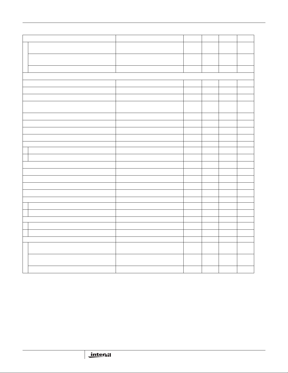
Electrical Specifications V
PARAMETER TEST CONDITIONS MIN TYP MAX UNITS
Input Low Voltage, V
Input High Voltage, V
Input Resistance to V
ICM7216D
Operating Supply Current, I
Supply Voltage Range (V
Maximum Frequency INPUT A, Pin 28, f
Maximum Oscillator Frequency and External Oscillator
Frequency, f
Minimum External Oscillator Frequency, f
Oscillator Transconductance, g
Multiplex Frequency, f
Time Between Measurements f
Input Voltages: Pins 12, 27, 28
Input Low Voltage, V
Input High Voltage, V
Input Resistance to V
Input Leakage, Pins 27, 28, I
Output Current, Pin 2, I
Output Current, Pin 2, I
Input Rate of Change, dVlN/dt Supplies Well Bypassed - 15 - mV/µs
Digit Driver: Pins 3, 4, 5, 6, 8, 9, 10, 11
Low Output Current, I
High Output Current, I
Segment Driver: Pins 15, 16, 17, 19, 20, 21, 22, 23
High Output Current, I
Leakage Current, I
Multiplex Inputs: Pins 1, 13, 14
Input Low Voltage, V
Input High Voltage, V
Input Resistance to VDD, R
OSC
INL
lNH
,
DD
DD
-V
DD
MUX
INL
INH
Pins 12, 24, R
DD,
ILK
OL
OH
OL
OH
OH
SLK
lNL
INH
R
= 5.0V, VSS = 0V, TA = 25oC, Unless Otherwise Specified (Continued)
DD
V
= V
IN
SS
), V
SUPPLY
lN
Display Off, Unused Inputs to V
INPUT A Frequency at f
A(MAX)
Figure 6 10 - - MHz
-2.5V 100 360 - k
DD
SS
MAX
OSC
V
M
IN
lN
= 4.75V, T
DD
f
= 10MHz - 500 - Hz
OSC
= 10MHz - 200 - ms
OSC
V
= V
IN
DD
VOL = +0.4V 0.36 - - mA
VOH = VDD -0.8V 265 - -
V
= +1.3V 50 75 - mA
OUT
V
= VDD -2.5V - 100 -
OUT
V
= VDD -2.0V 10 15 mA
OUT
V
= VDD -2.5V - - 10 µA
OUT
VIN = VDD -1.0V 100 360 - kΩ
= 85°C 2000 - -
A
-1.0V 100 400 - k
--V
V
-
DD
0.8
-25mA
4.75 - 6.0 V
10 - - MHz
--100 kHz
--1.0 V
3.5 - - V
--20
--V
VDD -
0.8
--V
--V
DD
2.0
DD
2.0
-
V
µ S
µ
µ
µ
-
V
Ω
Ω
A
A
A
5
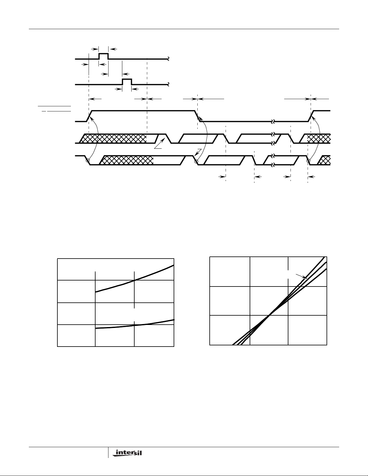
Timing Diagram
85oC
-20oC
4.5 ≤ VDD ≤ 6V
30
20
10
0
0 123
V
DD-VOUT
(V)
I
SEG
(mA)
25oC
INTERNAL
STORE
ICM7216B
40ms
30ms TO 40ms
INTERNAL
RESET
UPDATE
190ms TO 200ms
MEASUREMENT
IN PROGRESS
(INTERNAL ON
7216B)
INPUT A
INPUT B
NOTE:
60ms
40ms
FUNCTION:
TIME INTERVAL
PRIMING
PRIMING EDGES
MEASUREMENT INTERVAL
250ns MIN
MEASURED
INTERVAL
(FIRST)
MEASURED
INTERVAL
(LAST)
5. If range is set to 1 event, first and last measured interval will coincide.
FIGURE 1. WAVEFORMS FOR TIME INTERVAL MEASUREMENT (OTHERS ARE SIMILAR, BUT WITHOUT PRIMING PHASE)
Typical Performance Curves
UPDATE
20
15
10
FREQUENCY (MHz)
5
0
34 5 6
fA (MAX) FREQUENCY UNIT COUNTER,
T
= 25oC
A
FREQUENCY RATIO MODES
fA (MAX) fB (MAX) PERIOD,
TIME INTERVAL MODES
V
DD-VSS
(V)
FIGURE 2. fA(MAX), fB(MAX) AS A FUNCTION OF SUPPLY
FIGURE 3. TYPICAL I
SEG
vs VDD-V
OUT
6
 Loading...