Intersil Corporation ICL8052, ICL8068, ICL71C03 Datasheet
3-34
Features
• Typically Less Than 2µV
P-P
Noise (200.00mV Full
Scale, lCL8068)
• Accuracy Guaranteed to ±1 Count Over Entire ±20,000
Counts (2.0000V Full Scale)
• Guaranteed Zero Reading for 0V Input
• True Polarity at Zero Count for Precise Null Detection
• Single Reference Voltage Required
• Over-Range and Under-Range Signals Available for
Auto-Ranging Capability
• All Outputs TTL Compatible
• Medium Quality Reference, 40ppm (Typ) on Board
• Blinking Display Gives Visual Indication of Over
Range
• Six Auxiliary Inputs/Outputs are Available for
Interfacing to UARTs, Microprocessors or Other
Complex Circuitry
• 5pA Input Current (Typ) (8052A)
Description
The ICL8052 or ICL8068/lCL71C03 chip pairs with their
multiplexed BCD output and digit drivers are ideally suited
for the visual display DVM/DPM market. The outstanding
4
1
/2 digit accuracy, 200.00mV to 2.0000V full scale capability, auto-zero and auto-polarity combine with true ratiometric
operation, almost ideal differential linearity and time-proven
dual slope conversion. Use of these chip pairs eliminates
clock feedthrough problems, and avoids the critical board
layout usually required to minimize charge injection.
When only 2000 counts of resolution are required, the 71C03
can be wired for 3
1
/2 digits and give up to 30 readings/sec.,
making it ideally suited for a wide variety of applications.
The ICL71C03 is an improved CMOS plug-in replacement for
the lCL7103 and should be used in all new designs.
Pinouts
Ordering Information
PART NUMBER
TEMP.
RANGE (oC) PACKAGE
PKG.
NO.
ICL8052CPD 0 to 70 14 Ld PDIP E14.3
lCL8052CDD 0 to 70 14 Ld CERDIP F14.3
lCL8052ACPD 0 to 70 14 Ld PDIP E14.3
ICL8052ACDD 0 to 70 14 Ld CERDIP F14.3
ICL8068CDD 0 to 70 14 Ld CERDIP F14.3
ICL8068ACDD 0 to 70 14 Ld CERDIP F14.3
lCL8068ACJD 0 to 70 14 Ld CERDIP F14.3
ICL71C03CPl 0 to 70 28 Ld PDIP E28.6
lCL71C03ACPl 0 to 70 28 Ld PDIP E28.6
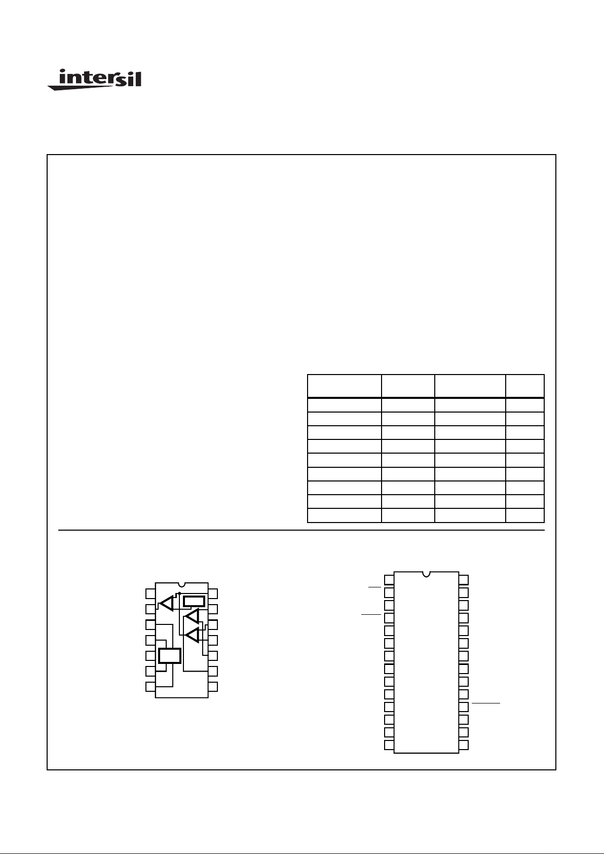
ICL8052/ICL8068
(CERDIP, PDIP)
TOP VIEW
ICL71C03 (PDIP)
TOP VIEW
V-
COMP OUT
REF CAP
REF BYPASS
GND
REF OUT
REF SUPPLY
INT OUT
+BUFF IN
+INT IN
-INT IN
-BUFF IN
BUFF OUT
V++
1
2
3
4
5
6
7
14
13
12
11
10
9
8
-1.2V
V
REF
ICL8052/
ICL8068
V+
4
1
/2/ 31/
2
POL
RUN/
HOLD
COMP IN
V-
REFERENCE
REF. CAP. 1
REF. CAP. 2
ANALOG IN
ANALOG GND
CLOCK IN
UNDER-RANGE
OVER-RANGE
BUSY
D
2
D
3
D
4
B8 (MSB)
B
2
D5 (MSD)
STROBE
A-Z IN
A-Z OUT
DIGITAL GND
D
1
(LSD)
B
4
B1 (LSB)
28
27
26
25
24
23
22
21
20
19
18
17
16
15
1
2
3
4
5
6
7
8
9
10
11
12
13
14
August 1997
ICL8052/ICL71C03,
ICL8068/ICL71C03
Precision 41/2 Digit, A/D Converter
File Number 3081.1
CAUTION: These devices are sensitive to electrostatic discharge; follow proper IC Handling Procedures.
http://www.intersil.com or 407-727-9207
| Copyright © Intersil Corporation 1999
3-35
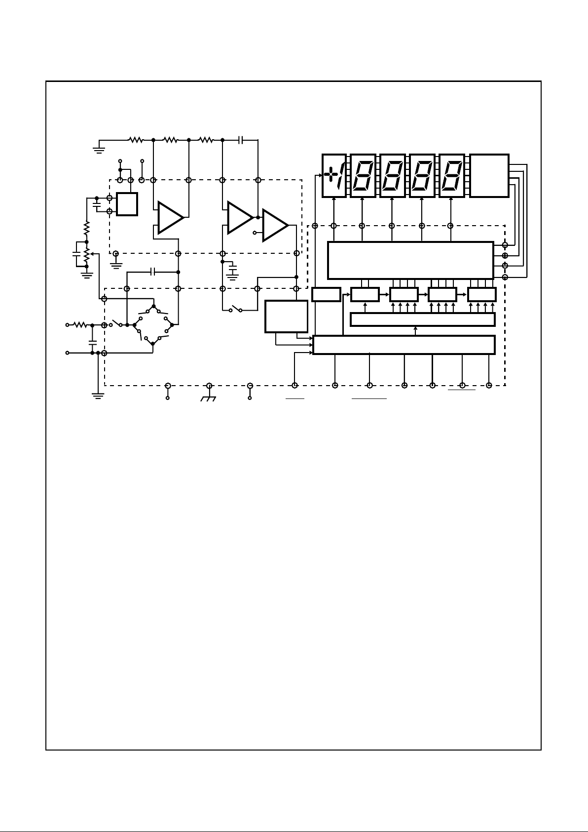
Functional Block Diagram
FIGURE 1.
A2
+
-
A3
+
-
INTEG.
COMP.
A1
+
-
BUFFER
14119
INT OUT-INT IN
BUF OUT
10
-BUF IN
-1.2V
2
1
-15V
78
+15V
12+INT IN
13
ICL8052/8068
INT.
REF.
6
3
+BUF IN
5
REF
OUT
10kΩ
1kΩ
300pF
10µF
COMP
OUT
COMP IN
516
9
MULTIPLEXER
COUNTERS
20
CONTROL LOGIC
ZERO
CROSSING
DETECTOR
21
22
23
ICL71C03
REF
AZ OUT
SW3
1
+5V
ANALOG
GND
ANALOG
INPUT
28
BUSY
18
STROBE
13
UNDER
1412
CLOCK24 1/2 DIGIT/
2
6
5
1
4
10µF (TYP)
CAP 2
REF
CAP 1
8
7
10
11
10kΩ
0.1µF
REF
1µF (TYP)
17
AZ IN
6
-15V
15
0.22µF
10kΩ 90kΩ 100kΩ
4
IN
RUN/
HOLD
RANGE
OVER
RANGE
3 1/2 DIGIT
B
1
B
2
B
3
B
4
LATCHLATCHLATCHLATCHLATCH
LSDMSD
SEVENSEGMENT
DECODER
3
POLARITY
19 24 25 26 27
D
5
D
4
D
3
D
2
D
1
ICL8052/ICL71C03, ICL8068/ICL71C03
3-36
Absolute Maximum Ratings Thermal Information
ICL8052, ICL8068
Supply Voltage . . . . . . . . . . . . . . . . . . . . . . . . . . . . . . . . . . . . . ±18V
Differential Input Voltage
(8068) . . . . . . . . . . . . . . . . . . . . . . . . . . . . . . . . . . . . . . . . . . ±30V
(8052) . . . . . . . . . . . . . . . . . . . . . . . . . . . . . . . . . . . . . . . . . . . ±6V
Input Voltage (Note 1). . . . . . . . . . . . . . . . . . . . . . . . . . . . . . . . ±15V
Output Short Circuit Duration All Outputs (Note 2). . . . . . . Indefinite
ICL71C03
Power Supply Voltage (GND to V+) . . . . . . . . . . . . . . . . . . . . . 6.5V
Negative Supply Voltage (GND to V-). . . . . . . . . . . . . . . . . . . . .-17V
Analog Input Voltage (Note 3) . . . . . . . . . . . . . . . . . . . . . . . V+ to V-
Digital Input Voltage (Note 4) . . . . . . . . (GND - 0.3V) to (V+ + 0.3V)
Operating Conditions
Temperature Range . . . . . . . . . . . . . . . . . . . . . . . . . . . .0oC to 70oC
Thermal Resistance (Typical, Note 5) θJA (oC/W) θJC (oC/W)
CERDIP Package . . . . . . . . . . . . . . . . 75 20
14 Ld PDIP Package. . . . . . . . . . . . . . 100 N/A
28 Ld PDIP Package. . . . . . . . . . . . . . 65 N/A
Maximum Storage Temperature . . . . . . . . . . . . . . . .-65oC to 150oC
Maximum Lead Temperature (Soldering, 10s) . . . . . . . . . . . .300oC
CAUTION: Stresses above those listed in “Absolute Maximum Ratings” may cause permanent damage to the device. This is a stress only rating and operation
of the device at these or any other conditions above those indicated in the operational sections of this specification is not implied.
NOTES:
1. For supply voltages less than ±15V, the absolute maximum input voltage is equal to the supply voltage.
2. Short circuit may be to ground or either supply. Rating applies to 70oC ambient temperature.
3. Input voltages may exceed the supply voltages provided the input current is limited to ±100µA.
4. Connecting any digital inputs or outputs to voltages greater then V+ or less than GND may cause destructive device latchup. For this
reason it is recommended that the power supply to the ICL71C03 be established before any inputs from sources not on that supply are
applied.
5. θJA is measured with the component mounted on an evaluation PC board in free air.
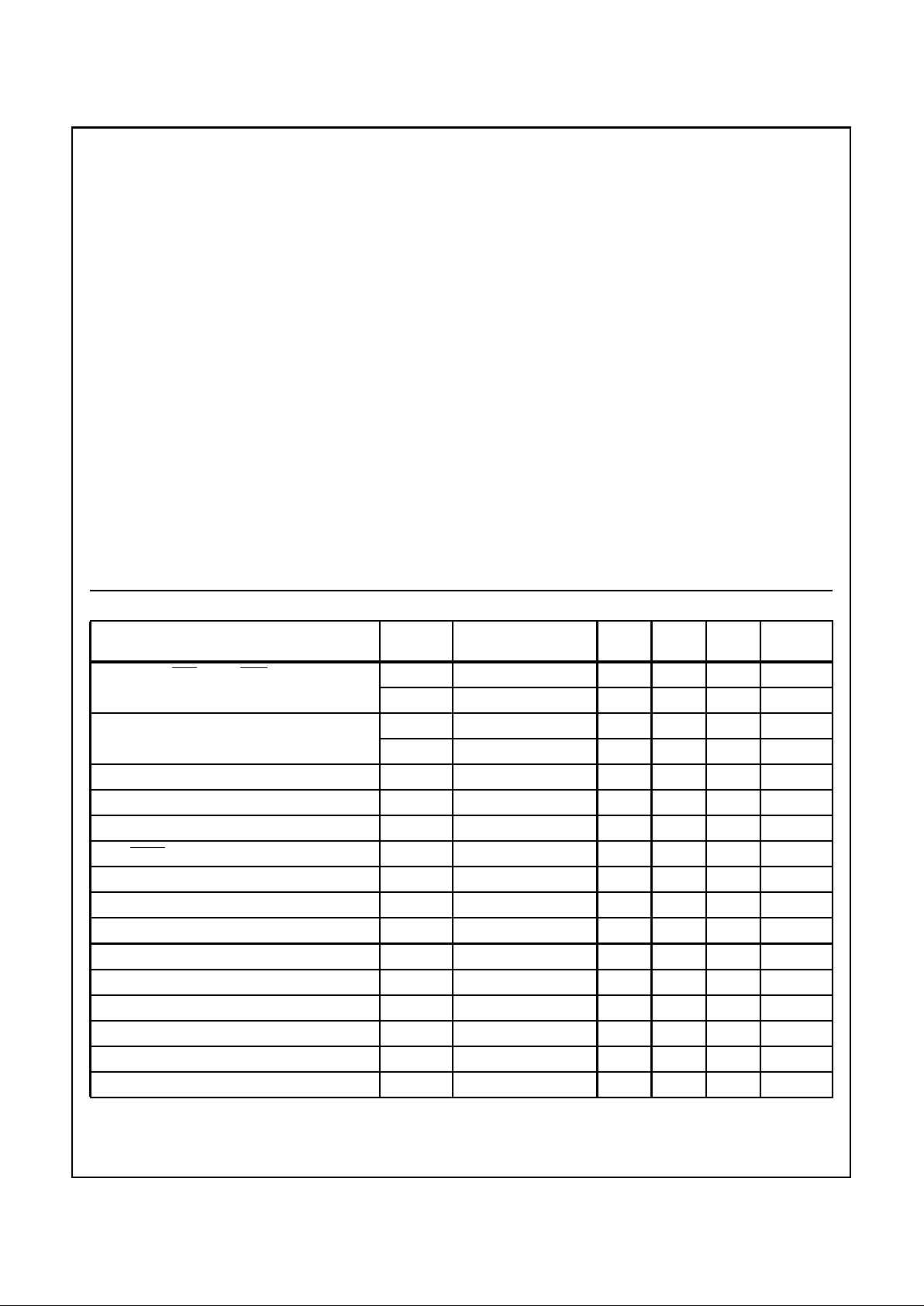
Electrical Specifications
PARAMETER SYMBOL
TEST
CONDITIONS MIN TYP MAX UNITS
Clock In, Run/Hold, 4 1/2 / 3 1/2 I
INL
VIN = 0 - 0.2 0.6 mA
I
INH
VIN = +5V - 0.1 10 µA
Comp. In Current I
INL
VIN = 0 - 0.1 10 µA
I
INH
VIN = +5V - 0.1 10 µA
Threshold Voltage V
INTH
- 2.5 - V
All Outputs V
OL
IOL = 1.6mA - 0.25 0.40 V
B1, B2, B4, B8,D1, D2, D3, D4, D
5
V
OH
IOH = -1mA 2.4 4.2 - V
Busy, Strobe, Over-Range, Under-Range Polarity V
OH
IOH = -10µA 4.9 4.99 - V
Switches 1, 3, 4, 5, 6 r
DS(ON)
- 400 - Ω
Switch 2 r
DS(ON)
- 1200 - Ω
Switch Leakage (All) I
D(OFF)
-2- pA
+5V Supply Range V+ 4 5 6 V
-15V Supply Range V- -5 -15 -18 V
+5V Supply Current I+ f
CLK
= 0 - 1.1 3 mA
-15V Supply Current I- f
CLK
= 0 - 0.8 3 mA
Power Dissipation Capacitance C
PD
vs Clock Frequency - 40 - pF
Clock Frequency (Note 6) DC 2000 1200 kHz
NOTE:
6. This specification relates to the clock frequency range over which the ICL71C03(A) will correctly perform its various functions. See the
“Max Clock Frequency” section under Component Value Selection for limitations on the clock frequency range in a system.
ICL8052/ICL71C03, ICL8068/ICL71C03
3-37
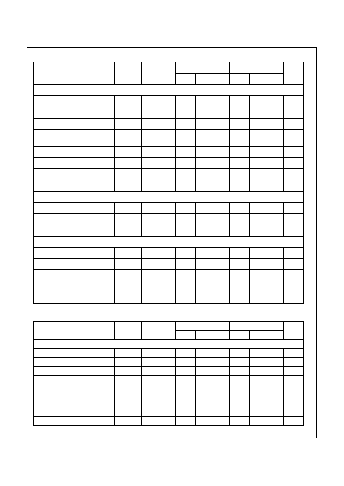
ICL8068 Electrical Specifications V
SUPPLY
= ±15V, TA = 25oC, Unless Otherwise Specified
PARAMETER SYMBOL
TEST
CONDITIONS
ICL8068 ICL8068A
UNITSMIN TYP MAX MIN TYP MAX
EACH OPERATIONAL AMPLIFIER
Input Offset Voltage V
OS
VCM = 0V - 20 65 - 20 65 mV
Input Current (Either Input) (Note 7) I
IN
VCM = 0V - 175 250 - 80 150 pA
Common-Mode Rejection Ratio CMRR VCM = ±10V 70 90 - 70 90 - dB
Non-Linear Component of CommonMode Rejection Ratio (Note 8)
VCM = ±2V - 110 - - 110 - dB
Large Signal Voltage Gain A
V
RL = 50kΩ 20,000 - - 20,000 - - V/V
Slew Rate SR - 6 - - 6 - V/µs
Unity Gain Bandwidth GBW - 2 - - 2 - MHz
Output Short-Circuit Current I
SC
-5--5-mA
COMPARATOR AMPLIFIER
Small-Signal Voltage Gain A
VOL
RL = 30kΩ - - 4000 - - - V/V
Positive Output Voltage Swing +V
O
12 13 - 12 13 - V
Negative Output Voltage Swing -V
O
-2.0 -2.6 - -2.0 -2.6 - V
VOLTAGE REFERENCE
Output Voltage V
O
1.5 1.75 2.0 1.60 1.75 1.90 V
Output Resistance R
O
-5--5-Ω
Temperature Coefficient TC - 50 - - 40 - ppm/oC
Supply Voltage (V++ -V-) V
SUPPLY
±10 - ±16 ±10 - ±16 V
Supply Current Total I
SUPPLY
- - 14 - 8 14 mA
ICL8052 Electrical Specifications V
SUPPLY
= ±15V, TA = 25oC, Unless Otherwise Specified
PARAMETER SYMBOL
TEST
CONDITIONS
ICL8052 ICL8052A
UNITSMIN TYP MAX MIN TYP MAX
EACH OPERATIONAL AMPLIFIER
Input Offset Voltage V
OS
VCM = 0V - 20 75 - 20 75 mV
Input Current (Either Input) (Note 7) I
IN
VCM = 0V - 5 50 - 2 10 pA
Common-Mode Rejection Ratio CMRR VCM = ±10V 70 90 - 70 90 - dB
Non-Linear Component of Common-
Mode Rejection Ratio (Note 8)
VCM = ±2V - 110 - - 110 - dB
Large Signal Voltage Gain A
V
RL = 50kΩ 20,000 - - 20,000 - - V/V
Slew Rate SR - 6 - - 6 - V/µs
Unity Gain Bandwidth GBW - 1 - - 1 - MHz
Output Short-Circuit Current I
SC
-20- -20-mA
ICL8052/ICL71C03, ICL8068/ICL71C03
3-38
COMPARATOR AMPLIFIER
Small-Signal Voltage Gain A
VOL
RL = 30kΩ - 4000 - - - - V/V
Positive Output Voltage Swing +V
O
12 13 - 12 13 - V
Negative Output Voltage Swing -V
O
-2.0 -2.6 - -2.0 -2.6 - V
VOLTAGE REFERENCE
Output Voltage V
O
1.5 1.75 2.0 1.60 1.75 1.90 V
Output Resistance R
O
-5--5-Ω
Temperature Coefficient TC - 50 - - 40 - ppm/oC
Supply Voltage (V++ -V-) V
SUPPLY
±10 - ±16 ±10 - ±16 V
Supply Current Total I
SUPPLY
- 6 12 - 6 14 mA
NOTES:
7. The input bias currents are junction leakage currents which approximately double for every 10oC increase in the junction temperature,
TJ. Due to limited production test time, the input bias currents are measured with junctions at ambient temperature. In normal
operation the junction temperature rises above the ambient temperature as a result of internal power dissipation, PD.
TJ=TA+R
θJAPD
, where R
θJA
is the thermal resistance from junction to ambient. A heat sink can be used to reduce temperature rise.
8. This is the only component that causes error in dual-slope converter.
System Electrical Specifications: ICL8068/ICL71C03
V++ = +15V, V+ = +5V, V- = -15V, TA = 25oC, f
CLK
Set for 3 Readings/Sec.
PARAMETER
TEST
CONDITIONS
ICL8068A/ICL71C03
(NOTE 9)
ICL8068A/ICL71C03
(NOTE 10)
UNITSMIN TYP MAX MIN TYP MAX
Zero Input Reading VIN = 0V,
Full Scale = 200mV
-000.0 ±000.0 +000.0 -000.0 ±000.0 000.0 Digital
Reading
Ratiometric Error (Note 11) VIN = V
REF
Full Scale = 2V
0.999 1.000 1.001 0.9999 1.0000 1.0001 Digital
Reading
Linearity Over ± Full Scale (Error of
Reading from Best Straight Line)
-2V ≤ VIN≤ +2V - 0.2 1 - 0.5 1 Counts
Differential Linearity (Difference
between Worst Case Step of Adjacent
Counts and Ideal Step)
-2V ≤ VIN≤ +2V - 0.01 - - 0.01 - Counts
Rollover Error (Difference in Reading
for Equal Positive & Negative Voltage
Near Full Scale)
-VIN≅ +VIN≈ 2V - 0.2 1 - 0.5 1 Counts
Noise (P-P Value Not Exceeded 95%
of Time)
VIN = 0V,
Full Scale = 200mV
-3--2- µV
Leakage Current at Input VIN = 0V - 200 300 - 100 200 pA
Zero Reading Drift (Note 12) VIN = 0V,
0oC ≤ TA ≤ 50oC
- 1 5 - 0.5 2 µV/oC
Scale Factor Temperature Coefficient
(Note 12)
VIN = 2V,
0oC ≤ TA ≤ 50oC
Ext. Ref. 0ppm/oC
- 3 15 - 2 5 ppm/oC
ICL8052 Electrical Specifications V
SUPPLY
= ±15V, TA = 25oC, Unless Otherwise Specified (Continued)
PARAMETER SYMBOL
TEST
CONDITIONS
ICL8052 ICL8052A
UNITSMIN TYP MAX MIN TYP MAX
ICL8052/ICL71C03, ICL8068/ICL71C03
3-39
Detailed Description
ANALOG SECTION
Figure 2 shows the equivalent Circuit of the Analog Section
of both the ICL71C03/8052 and the ICL71C03/8068 in the 3
different phases of operation. IF the RUN/HOLD pin is left
open or tied to V+, the system will perform conversions at a
rate determined by the clock frequency: 40,0002 at 4
1
/2 digit
and 4002 at 3
1
/2 digit clock periods per cycle (see Figure 3
for details of conversion timing).
Auto-zero Phase I (Figure 2A)
During the Auto-Zero, the input of the buffer is connected to
V
REF
through switch 2, and switch 3 closes a loop around
the integrator and comparator, the purpose of which is to
charge the auto-zero capacitor until the integrator output
does not change with time. Also, switches 1 and 2 recharge
the reference capacitor to V
REF
.
Input Integrate Phase II (Figure 2B)
During Input Integrate the auto-zero loop is opened and the
ANALOG INPUT is connected to the BUFFER INPUT
through switch 4 and C
REF
. If the input signal is zero, the
buffer, integrator and comparator will see the same voltage
that existed in the previous state (Auto-Zero). Thus, the
integrator output will not change but will remain stationary
during the entire Input Integrate cycle. If V
IN
is not equal to
zero, and unbalanced condition exists compared to the Auto
Zero phase, and the integrator will generate a ramp whose
slope is proportional to V
IN
. At the end of this phase, the
sign of the ramp is latched into the polarity F/F.
Deintegrate Phase II (Figures 2C and 2D)
During the Deintegrate phase, the switch drive logic uses the
output of the polarity F/F in determining whether to close
switch 6 or 5. If the input signal is positive, switch 6 is closed
and a voltage which is V
REF
more negative than during
Auto-Zero is impressed on the BUFFER INPUT. Negative
Inputs will cause +2(V
REF
) to be applied to the BUFFER
INPUT via switch 5. Thus, the reference capacitor generates
the equivalent of a (+) or (-) reference from the single
reference voltage with negligible error. The reference voltage
returns the output of the integrator to the zero-crossing point
established in Phase I. The time, or number of counts,
required to do this is proportional to the input voltage. Since
the Deintegrate phase can be twice as long as the Input
Integrate Phase, the input voltage required to give a full
scale reading is 2V
REF
.
System Electrical Specifications: ICL8052/ICL71C03
V++ = +15V, V+ = +5V, V- = -15V, TA = 25oC, f
CLK
Set for 3 Reading/Sec.
PARAMETER
TEST
CONDITIONS
ICL8068A/ICL71C03
(NOTE 9)
ICL8068A/ICL71C03
(NOTE 10)
UNITSMIN TYP MAX MIN TYP MAX
Zero Input Reading VIN = 0V,
Full Scale = 2V
-0.000 ±0.000 +0.000 -0.000 ±0.000 0.000 Digital
Reading
Ratiometric Error (Note 11) VIN = V
REF
Full Scale = 2V
0.999 1.000 1.001 0.9999 1.0000 1.0001 Digital
Reading
Linearity Over ± Full Scale (Error of
Reading from Best Straight Line)
-2V ≤ VIN≤ +2V - 0.2 1 - 0.5 1 Counts
Differential Linearity (Difference
between Worst Case Step of Adjacent
Counts and Ideal Step)
-2V ≤ VIN≤ +2V - 0.01 - - 0.01 - Counts
Rollover Error (Difference in Reading
for Equal Positive & Negative Voltage
Near Full Scale)
-VIN≅ +VIN≈ 2V - 0.2 1 - 0.5 1 Counts
Noise (Peak-To-Peak Value Not
Exceeded 95% of Time)
VIN = 0V,
Full Scale = 200mV,
Full Scale = 2V
-2050-
-
-
-30--
µV
Leakage Current at Input VIN = 0V - 5 30 - 3 10 pA
Zero Reading Drift VIN = 0V,
0oC To 70oC
- 1 5 - 0.5 2 µV/oC
Scale Factor Temperature Coefficient VIN = 2V,
0oC To 70oC,
Ext. Ref. 0ppm/oC
- 3 15 - 2 5 ppm/oC
NOTES:
9. Tested in 31/2 digit (2,000 count) circuit shown in Figure 5, clock frequency 12kHz. Pin 2 71C03 connected to GND.
10. Tested in 41/2 digit (20,000 count) circuit shown in Figure 5, clock frequency 120kHz. Pin 2 71C03A open.
11. Tested with a low dielectric absorption integrating capacitor. See Component Selection Section.
12. The temperature range can be extended to 70oC and beyond if the Auto-Zero and Reference capacitors are increased to absorb the high
temperature leakage of the 8068.
ICL8052/ICL71C03, ICL8068/ICL71C03
 Loading...