Intersil Corporation ICL8048 Datasheet

ICL8048
Data Sheet August 1999
Log Amplifier
The ICL8048 is a monolithic logarithmic amplifier capable of
handling six decades of current input, or three decades of
voltage input. It is fully temperature compensated and is
nominally designed to provide 1V of output for each decade
change of input. For increased flexibility, the scale factor,
reference current and offset voltage are externally
adjustable.
Ordering Information
PART
NUMBER
ICL8048BCJE 30mV 0 to 70 16 Ld CERDIP F16.3
ERROR
(25oC)
TEMPERA TURE
RANGE (oC) PACKAGE
PKG.
NO.
Pinout
ICL8048
(CERDIP)
TOP VIEW
File Number 2865.2
Features
• Full Scale Accuracy . . . . . . . . . . . . . . . . . . . . . . . . . 0.5%
o
• Temperature Compensated Operation. . . . . . 0
C to 70oC
• Scale Factor, Adjustable. . . . . . . . . . . . . . . . . 1V/Decade
• Dynamic Current Range. . . . . . . . . . . . . . . . . . . . . 120dB
• Dynamic Voltage Range. . . . . . . . . . . . . . . . . . . . . . 60dB
• Dual JFET Input Op Amps
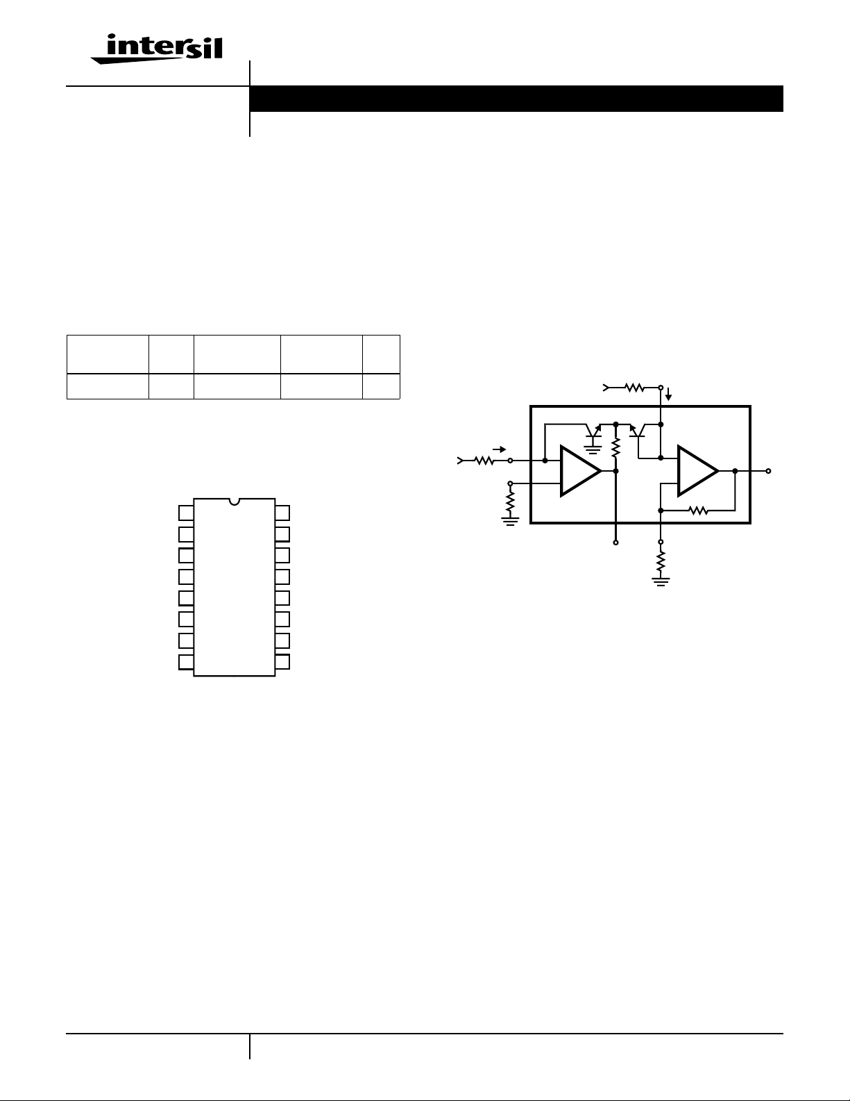
Functional Diagram
ICL8048
V
REF
Q
f
V
IN
IN
GND
2
1
-
A
1
+
Q
1
I
REF
16
2
+
A
2
-
V
OUT
10
OFFSET
A
1
A
OFFSET
1
OUTPUT
A
1
GND
NC
NULL
NULL
NC
1
2
I
IN
3
4
5
6
V-
7
8
16
I
REF
7
15
GAIN
A
14
NC
A
OFFSET
2
13
NULL
OFFSET
A
2
12
NULL
11
V+
10
V
OUT
9
NC
OUTPUT
1
15
GAIN
1
CAUTION: These devices are sensitive to electrostatic discharge; follow proper IC Handling Procedures.
1-888-INTERSIL or 321-724-7143
| Copyright © Intersil Corporation 1999

ICL8048
Absolute Maximum Ratings Thermal Information
Supply Voltage . . . . . . . . . . . . . . . . . . . . . . . . . . . . . . . . . . . . . . . . . ±18V
IIN (Input Current) . . . . . . . . . . . . . . . . . . . . . . . . . . . . . . . . . . . 2mA
I
(Reference Current). . . . . . . . . . . . . . . . . . . . . . . . . . . . . . 2mA
REF
Voltage Between Offset Null and V+ . . . . . . . . . . . . . . . . . . . . ±0.5V
Output Short Circuit Duration. . . . . . . . . . . . . . . . . . . . . . . Indefinite
Thermal Resistance (Typical, Note 1) θJA (oC/W) θJC (oC/W)
CERDIP Package. . . . . . . . . . . . . . . . . 75 22
Maximum Junction Temperature (Hermetic Package or Die) . . .175oC
Maximum Storage Temperature Range. . . . . . . . . . -65oC to 150oC
Maximum Lead Temperature (Soldering 10s) . . . . . . . . . . . . .300oC
Operating Conditions
Temperature Range . . . . . . . . . . . . . . . . . . . . . . . . . . . . 0oC to 70oC
CAUTION: Stresses above those listed in “Absolute Maximum Ratings” may cause permanent damage to the device. This is a stress only rating and operation of the
device at these or any other conditions above those indicated in the operational sections of this specification is not implied.
Die Characteristics
Number of Transistors or Gates. . . . . . . . . . . . . . . . . . . . . . . . . . . 62
NOTE:
1. θJA is measured with the component mounted on an evaluation PC board in free air.
Electrical Specifications V
= ±15V, TA = 25oC, I
S
= 1mA, Scale Factor Adjusted for 1V/Decade, Unless Otherwise Specified
REF
ICL4048BC
PARAMETER TEST CONDITIONS
UNITSMIN TYP MAX
Dynamic Range
(1nA - 1mA) RIN = 10kΩ 120 - - dB
I
IN
VIN (10mV - 10V) 60 - - dB
Error, % of Full Scale IIN = 1nA to 1mA - 0.20 0.5 %
TA = 0oC to 70oC,
- 0.60 1.25 %
IIN = 1nA to 1mA
Error, Absolute Value IIN = 1nA to 1mA - 12 30 mV
TA = 0oC to 70oC,
-3675 mV
IIN = 1nA to 1mA
Temperature Coefficient of V
OUT
IIN = 1nA to 1mA - 0.8 - mV/oC
Power Supply Rejection Ratio Referred to Output - 2.5 - mV/V
Offset Voltage (A1 and A2) Before Nulling - 15 25 mV
Wideband Noise At Output, for IIN = 100µA - 250 - µV
RMS
Output Voltage Swing RL = 10kΩ±12 ±14 - V
RL = 2kΩ±10 ±13 - V
Power Consumption - 150 200 mW
Supply Current - 5 6.7 mA
Typical Performance Curves
+4
+3
+2
+1
0
-1
OUTPUT VOLTAGE (V)
-2
-3
-4
1mV 10mV 100mV 1V 10V
I
= 100nA
REF
INPUT VOLTAGE (V)
I
REF
I
= 10µA
REF
RIN = 10kΩ
= 1mA
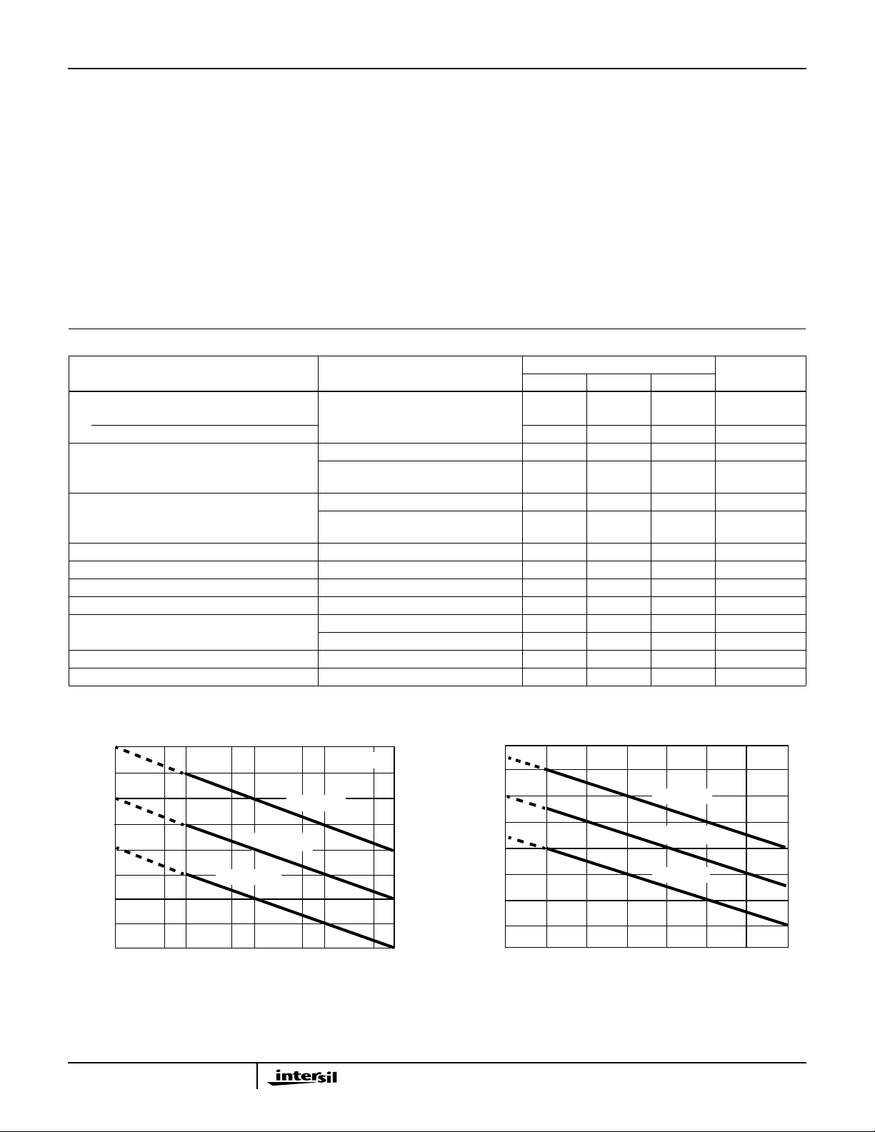
FIGURE 1. TRANSFER FUNCTION FOR VOLTAGE INPUTS FIGURE 2. TRANSFER FUNCTION FOR CURRENT INPUTS
2
+8
+6
+4
+2
0
-2
OUTPUT VOLTAGE (V)
-4
-6
-8
10
-10
I
= 1mA
REF
I
= 1µA
REF
I
= 1nA
REF
-9
-8
-7
-6
-5
10
10
10
10
10
INPUT CURRENT (A)
-4
10
-3
10

Typical Performance Curves (Continued)
ICL8048
100K
I
= 1mA
REF
10K
1K
100
SMALL SIGNAL BANDWIDTH (Hz)
10
-11
10
-9
10
INPUT CURRENT (A)
-7
10
-5
10
10
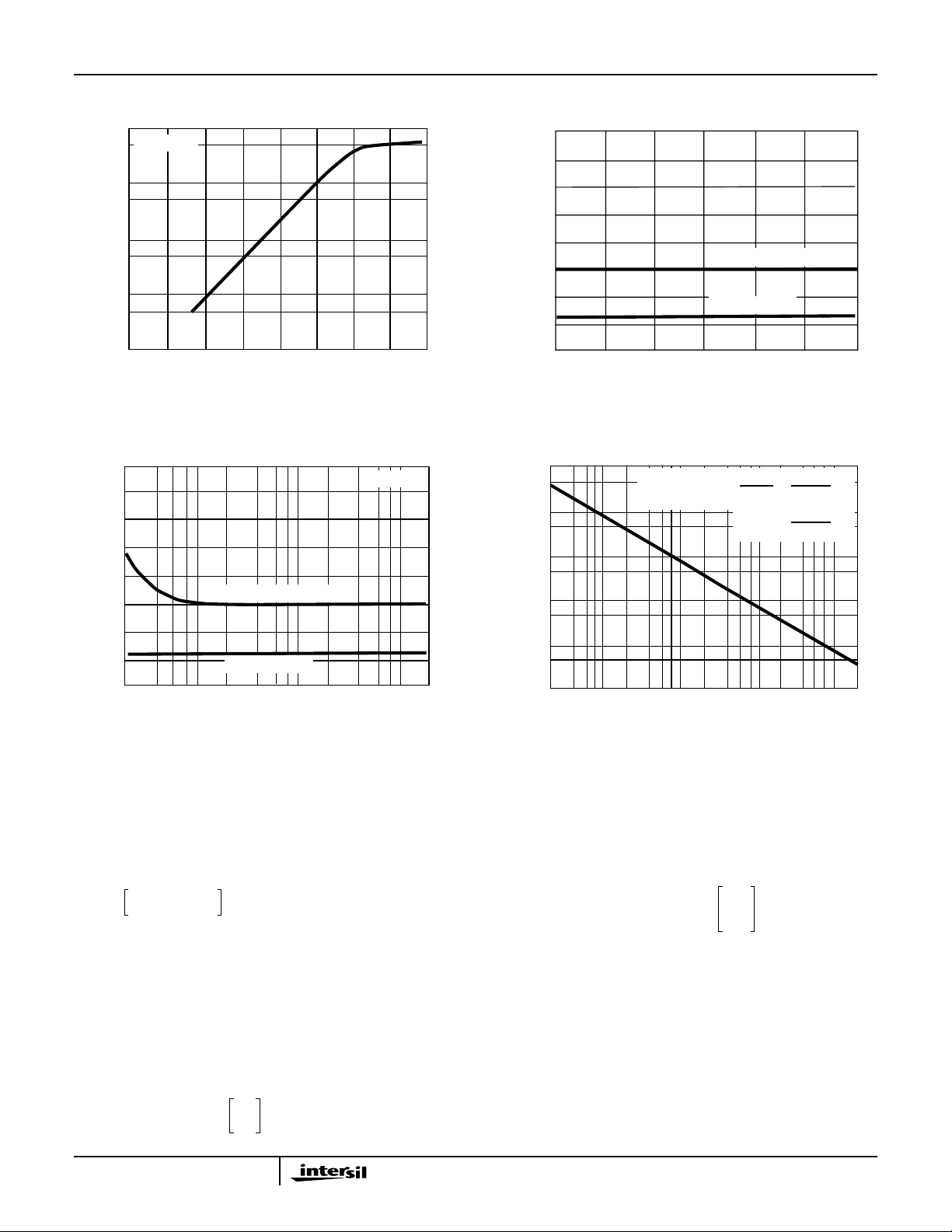
FIGURE 3. SMALL SIGNAL BANDWIDTHvs INPUT
CURRENT
200
175
150
125
100
75
50
25
MAXIMUM ERROR VOLTAGE (±mV)
0
10mV 100mV 1V 10V
8048BC (0oC TO 70oC)
8048BC (25oC)
INPUT VOLTAGE (V)
RIN = 10kΩ
FIGURE 5. MAXIMUM ERROR VOLTAGEAT THE OUTPUT vs
INPUT VOLTAGE
200
175
150
125
100
75
50
25
MAXIMUM ERROR VOLTAGE (±mV)
-3
0
-9
10
-8
10
-7
10
INPUT CURRENT (A)
8048BC (0oC TO 70oC)
8048BC (25oC)
-6
10
-5
10
-4
10
-3
10
FIGURE 4. MAXIMUM ERROR VOLTAGEAT THE OUTPUT vs
INPUT CURRENT
1000
434
100
10
1
VOLTAGE GAIN
0.1
0.01
1mV 10mV 100mV 1V 10V
R
= 10kΩ
IN
INPUT VOLTAGE (V)
∆V
∆V
IN
OUT
=VOLTAGE GAIN =
=
log10 e
V
IN
4343
V
IN
V
/
V
FIGURE 6. SMALL SIGNAL VOLTAGEGAIN vs INPUT
VOLTAGE FOR RS = 10kΩ
ICL8048 Detailed Description
The ICL8048 relies for its operation on the well known
exponential relationship between the collector current and
the base emitter voltage of a transistor:
ICISexp
---------------
kT
1–=
qV
B
E
For base emitter voltages greater than 100mV, Equation 1
becomes
qV
BE
ICISexp
=
--------------- -
kT
From Equation 2, it can be shown that for two identical
transistors operating at different collector currents, the V
difference (∆VBE) is given by:
∆V
BE
=
-2.303
kT
------ -
× log
q
10
I
C1
---------
I
C2
3
(EQ. 1)
(EQ. 2)
(EQ. 3)
BE
Referring to Figure 7 it is clear that the potential at the
collector of Q
output voltage is ∆V
V
=
OUT
The expression has a numerical value of 59mV at
o
25
C; thus in order to generate 1V/decade at the output, the
ratio (R
1+R2
is equal to the ∆VBEbetween Q1and Q2. The
2
-2.303
multiplied by the gain of A2:
BE
R1R2+
--------------------- -
2.303
kT
------ -
log
R
2
kT
------ -
×
q
10
q
I
IN
--------------
I
REF
)/R2is chosen to be 16.9. For this scale factor
(EQ. 4)
to hold constant as a function of temperature, the
(R
)/R2 term must have a 1/T characteristic to
1+R2
compensate for kT/q.
In the ICL8048 this is achieved by making R
a thin film
1
resistor, deposited on the monolithic chip. It has a nominal
value of 15.9kΩ at 25
o
C, and its temperature coefficient is
 Loading...