ICL8013
Data Sheet April 1999
1MHz, Four Quadrant Analog Multiplier
The ICL8013 is a four quadrant analog multiplier whose
output is proportional to the algebraic product of two input
signals. Feedback around an internal op amp provides level
shifting and can be used to generate division and square
root functions. A simple arrangement of potentiometers may
be used to trim gain accuracy, offset voltage and
feedthrough performance. The high accuracy, wide
bandwidth, and increased versatility of the ICL8013 make it
ideal for all multiplier applications in control and
instrumentation systems. Applications include RMS
measuring equipment, frequency doublers, balanced
modulators and demodulators, function generators, and
voltage controlled amplifiers.
Ordering Information
MULTIPLI-
CATION
PART
NUMBER
ICL8013BCTX ±1% 0 to 70 10 Pin
ICL8013CCTX ±2% 0 to 70 10 Pin
ERROR
(MAX)
TEMP.
RANGE (oC) PKG
Metal Can
Metal Can
PKG.
NO.
T10.B
T10.B
File Number 2863.4
Features
• Accuracy. . . . . . . . . . . . . . . . . . . . . . . . ±1% (“B” Version)
• Input Voltage Range. . . . . . . . . . . . . . . . . . . . . . . . . ±10V
• Bandwidth. . . . . . . . . . . . . . . . . . . . . . . . . . . . . . . . . 1MHz
• Uses Standard ±15V Supplies
• Built-In Op Amp Provides Level Shifting, Division and
Square Root Functions
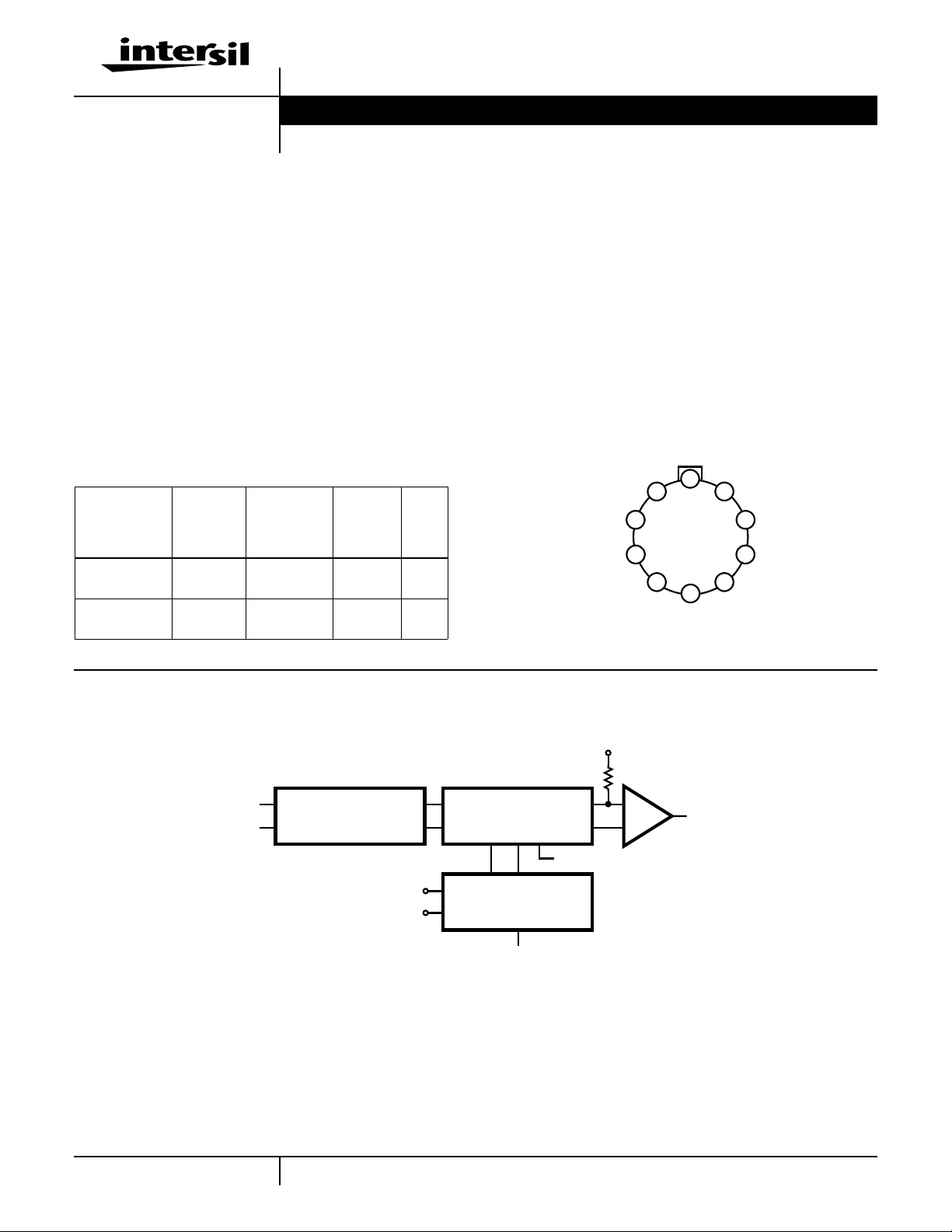
Pinout
ICL8013
(METAL CAN)
TOP VIEW
Y
OS
Y
V+
Z
IN
OUTPUT
10
1
IN
2
3
4
5
V-
Z
9
OS
GND
8
7
X
OS
6
X
IN
Functional Diagram
X
Z
IN
X
VOLTAGE TO CURRENT
IN
OS
CONVERTER AND
SIGNAL COMPRESSION
BALANCED
VARIABLE GAIN
AMPLIFIER
Z
OS
Y
IN
Y
OS
VOLTAGE TO CURRENT
CONVERTER
Z
IN
OP
AMP
OUT
1
CAUTION: These devices are sensitive to electrostatic discharge; follow proper IC Handling Procedures.
1-888-INTERSIL or 321-724-7143
| Copyright © Intersil Corporation 1999

ICL8013
Absolute Maximum Ratings Thermal Information
Supply Voltage. . . . . . . . . . . . . . . . . . . . . . . . . . . . . . . . . . . . . . ±18
Input Voltages (XIN, YIN, ZIN, XOS, YOS, ZOS) . . . . . . . . . V
SUPPLY
Operating Conditions
Temperature Range
ICL8013XC. . . . . . . . . . . . . . . . . . . . . . . . . . . . . . . . 0oC to 70oC
CAUTION: Stresses above those listed in “Absolute Maximum Ratings” may cause permanent damage to the device. This is a stress only rating and operation of the
device at these or any other conditions above those indicated in the operational sections of this specification is not implied.
NOTE:
1. θJA is measured with the component mounted on an evaluation PC board in free air.
Thermal Resistance (Typical, Note 1) θJA (oC/W) θJC (oC/W)
Metal Can Package . . . . . . . . . . . . . . . 160 75
Maximum Junction Temperature (Metal Can Package) . . . . . . .175oC
Maximum Storage Temperature Range. . . . . . . . . . -65oC to 150oC
Maximum Lead Temperature (Soldering 10s) . . . . . . . . . . . . 300oC
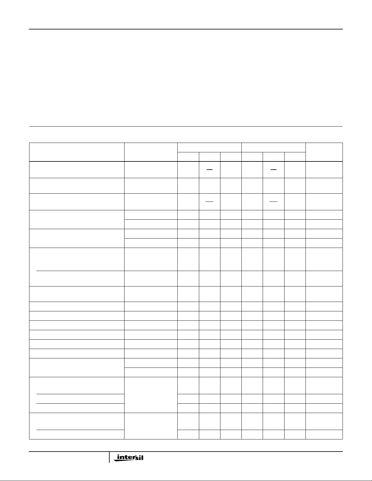
Electrical Specifications T
PARAMETER
Multiplier Function - XY
Multiplication Error -10 < X < 10
Divider Function - 10Z
Division Error X = -10 - 0.3 - - 0.3 - % Full Scale
Feedthrough X = 0, Y = ±10V - - 100 - - 200 mV
Non-Linearity
X Input X = 20V
Y Input Y = 20V
Frequency Response Small Signal
Bandwidth (-3dB)
Full Power Bandwidth - 750 - - 750 - kHz
Slew Rate - 45 - - 45 - V/µs
1% Amplitude Error - 75 - - 75 - kHz
1% Vector Error (0.5o Phase Shift) - 5 - - 5 - kHz
Settling Time (to ±2% of Final Value) VlN = ±10V - 1 - - 1 - µs
Overload Recovery (to ±2% of Final Value) VlN = ±10V - 1 - - 1 - µs
Output Noise 5Hz to 10kHz - 0.6 - - 0.6 - mV
Input Resistance VlN = 0V
X lnput - 10 - - 10 - MΩ
Y lnput - 6 - - 6 - MΩ
Z lnput - 36 - - 36 - kΩ
Input Bias Current VlN = 0V
X or Y Input - - 7.5 - - 10 µA
Z Input - 25 - - 25 - µA
= 25oC, V
A
Specified
= ±15V, Gain and Offset Potentiometers Externally Trimmed, Unless Otherwise
SUPPLY
TEST
CONDITIONS
-10 < Y < 10
X = -1 - 1.5 - - 1.5 - % Full Scale
Y = 0, X = ±10V - - 100 - - 150 mV
P-P
Y= ±10V
X = ±10V
5Hz to 5MHz - 3 - - 3 - mV
DC
P-P
DC
ICL8013B ICL8013C
UNITSMIN TYP MAX MIN TYP MAX
--XY10-
10
- - 1.0 - - 2.0 % Full Scale
- - 10Z
X
- ±0.5 - - ±0.8 - %
- ±0.2 - - ±0.3 - %
- 1.0 - - 1.0 - MHz
X
-
RMS
RMS
2

ICL8013
Electrical Specifications T
=25oC, V
A
= ±15V, Gain and Offset Potentiometers Externally Trimmed, Unless Otherwise Specified
SUPPLY
(Continued)
ICL8013B ICL8013C
UNITSMIN TYP MAX MIN TYP MAX
PARAMETER
TEST
CONDITIONS
Power Supply Variation
Multiplication Error - 0.2 - - 0.2 - %/%
Output Offset - - 75 - - 100 mV/V
Scale Factor - 0.1 - - 0.1 - %/%
Quiescent Current - 3.5 6.0 - 3.5 6.0 mA
THE FOLLOWING SPECIFICATIONS APPLY OVER THE OPERATING TEMPERATURE RANGES
Multiplication Error -10V < XIN < 10V,
- 2 - - 3 - % Full Scale
-10V < YIN < 10V
Average Temp. Coefficients
Accuracy - 0.06 - - 0.06 - %/oC
Output Offset - 0.2 - - 0.2 - mV/oC
Scale Factor - 0.04 - - 0.04 - %/oC
Input Bias Current VIN = 0V
X or Y Input - - 5 - - 10 µA
Z Input - - 25 - - 35 µA
Input Voltage (X, Y, or Z) - - ±10 - - ±10 V
Output Voltage Swing RL≥ 2kΩ
- ±10 - - ±10 - V
CL < 1000pF
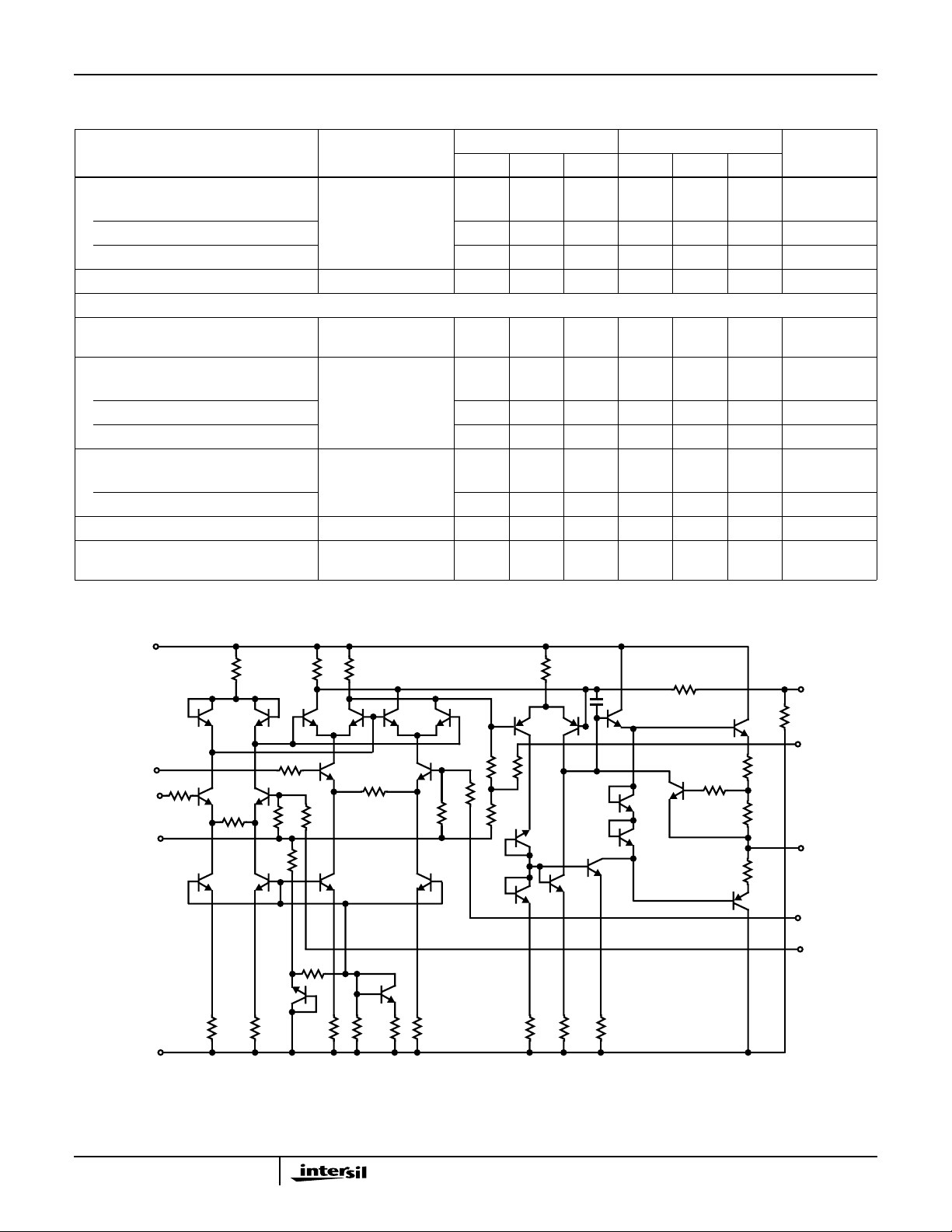
Schematic Diagram
V+
Q
1
Y
IN
R
1
X
COMMON
IN
V-
Q
3
R
Q5Q
R
4
R
2
Q
2
R
9
Q
4
3
R6R
R
10
6
R
Q
28
R
5
R
R
16
8
Q
8
Q
7
Q
9
R
7
Q
11
32
R
12
R
R
15
Q
15
Q
14
R
22
R
Q
10
13
Q
12
Q
13
11
20
R
17
R
R
19
R
18
21
R24R
R
23
C
1
Q
Q
17
Q
16
Q
18
Q
20
Q
19
25
21
Q
24
R
26
R
27
Q
25
R
R
Q
26
Q
22
Q
23
31
30
R
28
R
29
Q
27
R
33
OUTPUT
Z
IN
Z
OS
Y
OS
X
OS
3
 Loading...