

TM
R
R
ICL7673
Data Sheet April 1999
Automatic Battery Back-Up Switch
The Intersil ICL7673 is a monolithic CMOS battery backup
circuit that offers unique performance advantages over
conventional me ans of switching to a backup supply . The
ICL7673 is intended as a low-cost solution for the switching
of systems between two power supplies; main and battery
backup. The main appli cation is keep-al ive-battery power
switching for use in volatile CMOS RAM memory systems
and real time clocks. In many applications this circuit wi ll
represent a low insertion voltage loss between the supplies
and load. Thi s cir cuit feat ur es low cu rrent cons umption, wide
operating voltage range, and exce ptionally low leaka ge
between inputs. Lo gic output s are provi ded that c an be used
to indicate which supply is connected and can al so be used
to increase the power switching capability of the circuit by
driving external PNP transistors.
Ordering Information
PART
NUMBER
ICL7673CPA 0 to 70 8 Ld PDIP8 E8.3
ICL7673CBA 0
ICL7673ITV 25 to 8 5
TEMP. RANGE
o
(
C) PACKAGE PKG. NO.
to 70 8 Ld SOIC (N) M8.15
8 Ld Metal Can T8.C
Pinouts
ICL7673 (SOIC, PDIP)
TOP VIEW
FN3183.2
Features
• Automatically Connects Output to the Greater of Either
Input Sup ply Volt a ge
• If Main Power to External Equipment is Lost, Circuit Will
Automatically Connect Battery Backup
• Reconnects Main Power When Restored
• Logic Indicator Sig naling St atus of Main Power
• Low Impedance Connection Switches
• Low Internal Power Consumption
• Wide Supply Range: . . . . . . . . . . . . . . . . . . . 2.5V to 15V
• Low Leakage Between Inputs
• External Tr ansistors May Be Added if Very Large
Currents Need to Be Switched
Applications
• On Board Battery Backup for Real-Time Clocks,
Timers, or Volati le RAMs
• Over/Under Voltage Detector
• Peak Vol tage Detector
•Other Uses:
- Portable Instruments , Por table Tel ephones, Line
Operated Equipment
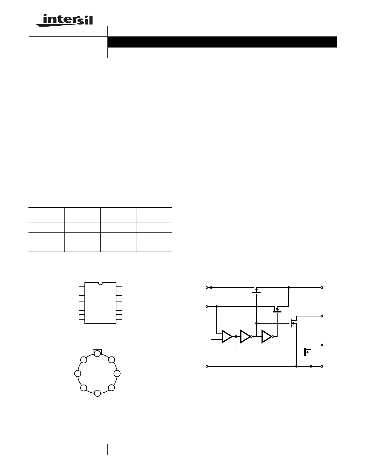
Functional Block Diagram
V
V
S
BAR
GDN
V
S
SBAR
1
O
2
S
3
4
ICL7673 (CAN)
TOP VIEW
V
1
O
2
3
V
P
8
4
GND
3-81
V
8
V
P
7
NC
6
P
BAR
5
NC
P
V
S
P1
P2
V
O
S
BA
-
+
NC
7
GND
PBAR
6
VP > VS, P1 SWITCH ON AND P
NC
5
CAUTION: These devices are sensitive to electrostatic discharge; follow proper IC Handling Procedures.
1-888-INTERSIL or 321-724-7143
V
> VP, P2 SWITCH ON AND S
S
| Intersil (and design) is a trademark of Intersil Americas Inc.
Copyright © Intersil Americas Inc. 2002. All Rights Reserved
SWITCH ON
BAR
SWITCH ON
BAR
P
BA
ICL7673
Absolute Maximum Ratings Thermal Information
Input Supply (VP or VS) Voltage . . . . . . . . . . . . GND - 0.3V to +18V
Output Voltages P
BAR
and S
. . . . . . . . . . .GND - 0.3V to +18V
BAR
Peak Current
Input V
Input V
P
(at VP = 5V) (Note 1) . . . . . . . . . . . . . . . . . . . . . . . 38mA
P
(at VS = 3V) . . . . . . . . . . . . . . . . . . . . . . . . . . . . . . 30mA
S
BAR
or S
. . . . . . . . . . . . . . . . . . . . . . . . . . . . . . . . . . 150mA
BAR
Thermal Resistance (Typical, Note 2) θ
PDIP Package . . . . . . . . . . . . . . . . . . . 150 N/A
Plastic SOIC Package . . . . . . . . . . . . . 180 N/A
Metal Can. . . . . . . . . . . . . . . . . . . . . . . 156 68
Maximum Storage Temperature. . . . . . . . . . . . . . . . -65
Maximum Lead T emperature (Soldering, 10sec). . . . . . . . . . .300
(SOIC - Lead Tips Only)
Operating C o ndi t io ns
Temperature Range:
ICL7673C. . . . . . . . . . . . . . . . . . . . . . . . . . . . . . . . . . . 0
ICL7673I. . . . . . . . . . . . . . . . . . . . . . . . . . . . . . . . . . -25
CAUTION: Stresses abo ve thos e lis ted in “A bsolut e Ma xi mum Rati ngs” may c ause perma nent damag e to the dev ice. T hi s is a stress onl y rating and operation of the
device at these or any other conditions above those indicated in the operational sections of this specification is not implied.
NOTES:
o
1. Derate above 25
is measured with t he compon ent mounted on an evaluation PC board in free air.
2. θ
JA
C by 0.38mA/oC.
o
C to 70oC
o
C to 85oC
(oC/W) θ
JA
(oC/W)
JC
o
C/W
o
C to 150oC
o
C
Electrical Specifications T
= 25oC Unle ss Otherwise S pecified
A
PARAMETER SYMBOL TEST CONDITIONS MIN TYP MAX UNITS
Input Voltage V
V
P
S
VS = 0V, I
VP = 0V, I
= 0mA 2.5 - 15 V
LOAD
= 0mA 2.5 - 15 V
LOAD
Quiescent Sup pl y C urr e nt I+ VP = 0V, VS = 3V, I
Switch Resistance P1 (Note 1) r
P1 VP = 5V, VS = 3V, I
DS(ON)
At T
= +85oC-16-Ω
A
VP = 9V, VS = 3V, I
V
= 12V, VS = 3V, I
P
Temperature Coefficient of Swit ch Resistance P1
Switch Resistance P2 (Note 1) r
T
C(P1)
DS(ON)
VP = 5V, VS = 3v, I
P2 VP = 0V, VS = 3V, I
At T
= +85oC-60-Ω
A
VP = 0V, VS = 5V, I
V
= 0V, VS = 9V, I
P
Temperature Coefficient of Swit ch Resistance P2
Leakage Current (V
to VS)I
P
Leakage Current (VP to VS)I
Open Drai n Out pu t Sa tu rat i on Vo lt ag es V
T
C(P2)
L(PS)
L(SP)
OPBARVP
VP = 0V, VS = 3V, I
VP = 5V, VS = 3V, I
At T
= +85oC-35-nA
A
VP = 0V, VS = 3V, I
at T
= + 85oC-120-nA
A
= 5V, VS = 3V, I
At TA = 85oC-120-mV
V
= 9V, VS = 3V, I
P
V
= 12V, VS = 3V, I
P
I
= 0mA
LOAD
= 0mA - 1.5 5 µA
LOAD
= 15mA - 8 15 Ω
LOAD
= 15mA - 6 - Ω
LOAD
= 15mA - 5 - Ω
LOAD
= 15mA - 0.5 - %/oC
LOAD
= 1mA - 40 100 Ω
LOAD
= 1mA - 26 - Ω
LOAD
= 1mA - 16 - Ω
LOAD
= 1mA - 0.7 - %/oC
LOAD
= 10mA - 0.01 20 nA
LOAD
= 10mA - 0.01 50 nA
LOAD
SINK
SINK
SINK
= 3.2mA, I
= 3.2mA, I
= 3.2mA
= 0mA - 85 400 mV
LOAD
= 0mA - 50 - mV
LOAD
-40- mV
3-82
ICL7673
Electrical Specifications T
= 25oC Unle ss Otherwise S pecified (Continued)
A
PARAMETER SYMBOL TEST CONDITIONS MIN TYP MAX UNITS
Open Drai n Out pu t Sa tu rat i on Vo lt ag es V
Output Leakage Currents of P
S
BAR
BAR
and
Switchover Uncertainty for Complete
Switch ing of Inputs and Open Drain
OSBARVP
I
LPBARVP
I
LSBARVP
V
- VSVS = 3V, I
P
= 0V, VS = 3V, I
at T
= + 85oC-210-mV
A
VP = 0V, VS = 5V, I
V
= 0V, VS = 9V, I
P
= 0V, VS = 15V, I
= 3.2mA, I
SINK
= 3.2mA I
SINK
= 3.2mA I
SINK
= 0mA - 50 500 nA
LOAD
= 0mA - 150 400 mV
LOAD
= 0mA - 85 - mV
LOAD
= 0mA - 50 - mV
LOAD
at TA = + 85oC-900-nA
= 15V, VS = 0V, I
at T
= + 85oC-900-nA
A
= 3.2mA, I
SINK
= 0mA - 50 500 nA
LOAD
= 15mA - ±10 ±50 mV
LOAD
Outputs
NOTE:
3. The Minimum input to output volt age can be determined by mult iplying the load current by the switch resistance.
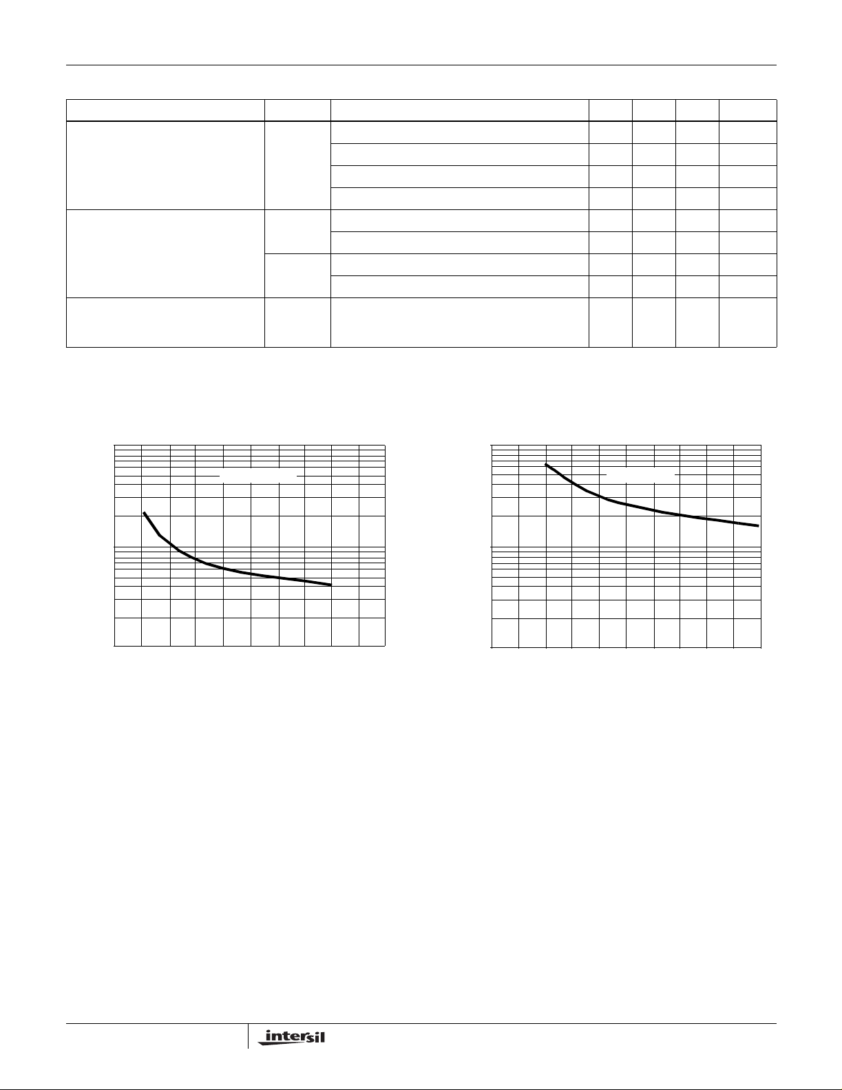
Typical Performance Curves
100
I
LOAD
= 15mA
100
I
LOAD
= 1mA
10
ON-RESISTANCE P1 (Ω)
1
02 46810121416
INPUT VOLTAGE VP (V)
FIGURE 1. ON-RESISTANCE SWITCH P1 AS A FUNCTION OF
INPUT VOLTAGE V
P
10
ON-RESISTANCE P2 (Ω)
1
0246810
INPUT VOLTAGE V
S
FIGURE 2. ON-RESISTANCE SWIT CH P2 AS A FUNCTION OF
INPUT VOLTAGE V
S
3-83

Typical Performance Curves (Continued)
I
LEAKAGE CURRENT
2
ICL7673
1
0.8
0.6
0.4
SUPPLY CURRENT (µA)
0.2
02 46 810121416
FIGURE 3. SUPPL Y CURRENT AS A FUNCTION OF SUPPL Y
VOLTAGE
1mA
100mA
10nA
1nA
S
1000pA
10pA
1pA
02456 8101
FIGURE 5. IS LEAKAGE CURRENT VP TO VS AS A
FUNCTION OF INPUT VOLTAGE
SUPPLY VOLTAGE (V)
I
= 10mA
LOAD
= 0V
V
S
INPUT VP (V)
-40oC
o
25
o
85
85oC
25oC
C
C
Detailed Description
As shown in the Func tional Di agr am, the I CL7673 inc ludes a
comparator whi ch senses the input vol tages V
output of the comparator drives the fi rst inverter and the
open-drain N-Channel transistor P
drives a large P-Channel switch, P
. The first inverter
BAR
, a second inverter, and
1
another open-dr ain N-Channel transist or , S
and VS. The
P
. The second
BAR
5
4
3
2
1
OUTPUT SATURATION VOLTAGE (V)
0 40 80 120 140 180
FIGURE 4. P
BAR
FUNCTION OF OUTPUT CURRENT
inverter drives another large P-Chan nel switch P
VO = 5V VO = 9V
VO = 3V
OUTPUT CURRENT (mA)
OR S
SATURATION VOLTA GE AS A
BAR
VO = 12V
VO = 15V
2
. The
ICL7673, connected to a main and a backup power supply,
will connect the supply of greater potential to its output. The
circuit provides break-before-make switch action as it
switches from main to backup power in the event of a main
power supply f ailur e. For proper o perati on, i nputs V
and VS
P
must not be allowed to float, and, the difference in the two
supplies must be greater than 50mV. The leakage current
through the rever se biased parasi ti c diode of switch P
is
2
very low.
Output Vo ltag e
The output operat ing voltage range is 2.5V to 15V. The
insertion loss between either input and the output is a
function of load current , inpu t volt ag e, and temper ature . This
is due to the P-Channels bei ng operated in their trio de
region, and, the ON-resistance of the switches is a function
of output voltage V
. The ON-resistance of the P-Channels
O
have positive temperature coef fi cients, and therefore as
temperature i ncreases the inserti on loss also increases. At
low load currents the output voltage is nearly equal to the
greater of the two inputs. The maximum voltage dr op across
switch P
or P2 is 0.5V, since above this voltage the body-
1
drain parasitic diode will become forward biased. Complete
switching of the inputs and open-drain outputs typi cally
occurs in 50µs.
Input Voltage
The input operating voltage range for VP or VS is 2.5V to
15V. The input supply voltage (V
limited to 2V per microsecond to avoid potent ial harm to the
circuit. In line-operated sys tems, th e ra te-of-rise (o r fall) of
the supply is a functi on of power supply design. For battery
applications it may be necessary to use a capacitor between
the input and ground pins to limit the rate-of-rise of the
or VS) slew rate sh ould be
P
3-84

ICL7673
supply volt age. A low-impedance cap acitor such as a
0.047µF disc ceram ic can be used to redu ce the rate-of-rise.
Status Indicator Outputs
The N-Channel open drain output transistors can be used to
indicate which supply is connected, or can be used to drive
external PNP transistors to increase the power switching
capab ility o f t h e circu it. When using exter n al PNP po w e r
transist ors, the output curren t is limited by the beta and
thermal characteristics of the powe r tr ansistors. The
application section detail s the use of external PNP
transistors.
Applications
A typical discrete battery backup circuit is illustrated in Figure
6. This approach r equir es several c om ponents, substa ntial
printed circuit board space, and high labor cost. It also
cons um es a fairly high quiesc ent current. The ICL7673
battery backup circuit, illustrated in Figure 7, will often replace
such discre te desi gns and offer much better performance,
higher reliability, and lower system manufacturing cost. A
trickle charge system could be implemented with an additional
resistor and diode as shown in Figure 8. A complete low
power AC to regulat ed DC system can be implem ented using
the ICL7673 and ICL7663S micropower voltage regulator as
shown in Figure 9.
+5V
PRIMARY
DC POWER
NiCAD
BATTERY
STACK
GND
FIGURE 6. DISCRETE BATTERY BACKUP CIRCUIT
V
O
+5V OR
+3V
STA T US
INDICATOR
+5V
PRIMARY
SUPPLY
LITHIUM
BATTERY
8
V
P
2
V
S
+
GND
Pbar
4
1
V
O
6
V
O
+5V OR +3V
R
I
STATUS
INDICATOR
-
GND
FIGURE 7. ICL7673 BA TTERY BACKUP CIRCUIT
+5V
PRIMARY
SUPPLY
R
C
RECHARGEABLE
BATTERY
GND
FIGURE 8. APPLICA TION REQUIRING RECHARGEABLE
BATTERY BACKUP
8
V
P
2
V
S
+
-
GND
1
V
4
O
V
O
+5V OR +3V
A typical a ppl ic at io n , as illus trated in Fig u re 12, w o ul d be a
microprocess or sy stem requi rin g a 5V supp ly. In the event of
primary supply failure, the system is powered down, and a
3V battery is employed to maintain clock or volatile memory
data. The main and backup supplies are connected to V
, with th e c ircuit o u tput VO supplying power to the
and V
S
P
clock or volatil e m em ory. The ICL7673 will sense the main
supply, when energized, to be of greater potential than V
and connect, via its intern al MOS switches, V
The backup input, V
will be disconnected in ternally. In the
S
to output VO.
P
S
event of main supply fai lure, the circuit wi ll sense that the
backup supply is now the greater potential, disconnect V
from V
, and connect VS.
O
P
Figure 11 illustrat es the use of external PNP power
transistors to increase the power switching capability of the
circuit. In t his application the output current is limited by the
beta and thermal characterist ics of the power transi stors.
Applications for the ICL7673 include volatile semiconductor
memory storage systems, real-time clocks, timers, alarm
systems, and over/under the voltage detectors. Other
systems requi ring DC po wer when t he master AC lin e su pply
fails can also use the ICL7673.
3-85
If hysteresis is desired for a par ticul ar low power appli cati on,
positive fe edback can be applied between the input V
open drain output S
through a resist or as i ll u strated in
BAR
and
P
Figure 12. For high power applications hys teresis can be
applied as shown in Figure 13.
The ICL7673 can also be used as a clipping circuit as
illustrated in Figure 14. With high impedance loads the
circuit ou tp ut w ill b e ne arl y equal to the greater of the two
input signals.

120/240
VAC
POWER
+5V
MAIN
ICL7673
FUSE
STEPDOWN
TRANSFORMER
BRIDGE
RECTIFIER
C
1
ICL7663
REGULATOR
FIGURE 9. POWER SUPPLY FOR LOW POWER PORTABLE AC TO DC SYSTEMS
POWER
FAIL
DETECTOR
INTERRUPT SIGNAL
MICROPROCESSOR
28
R
2
4
6
R
1
R
3
+
D
1
-
V
O
BACKUP CIRCUIT
V
P
V
S
BATTERY
STACK
V
ICL7673
ICL7673
BATTERY
BACK-UP
2
4
P
GND
V
18
V
S
O
+
MAIN
SUPPLY
3V
BACKUP
SUPPLY
VOLATILE
RAM
FIGURE 10. TYPICAL MI CRO PRO CESSO R ME MORY APPLICATION
R
2
V
P
8
ICL7673
V
S
23
+
-
GND
1
V
NC
O
P-
6
S-
R
1
PNP
R
R
(NOTE 4)
PNP
4
3
NOTE 4. > 1M
FIGURE 11. HIGH CURRENT BATTERY BACKUP SYSTEM
R
F
EXTERNAL
EQUIPMENT
W
-
MAIN
SUPPLY
R
S
BATTERY
BACKUP
V
P
8
ICL7673
V
S
+
23
S-
GND
V
O
-
GNDGND
FIGURE 12. LOW CURRENT BATTERY BACKUP SYSTEM WITH HYSTERESIS
3-86

ICL7673
+V
MAIN
SUPPLY
MAIN
SUPPLY
GND
R
2
R
+
-
R
S
BACKUP
SUPPLY
F
V
P
8
ICL7673
V
S
23
4
NC
1
P-
6
S-
R
1
FIGURE 13. HIGH CURRENT BACKUP SYSTEM WITH HYSTERESIS
V
P
ICL7673
V
S
GND
V
O
V
S
V
O
PNP
PNP
R
4
R
3
EXTERNAL
EQUIPMENT
V
P
FIGURE 14. CLIPPLING CIRCUITS
3-87
 Loading...