Intersil Corporation ICL7667 Datasheet

ICL7667
Data Sheet April 1999
Dual Power MOSFET Driver
The ICL7667 is a dual monolithic high-speed driver
designed to convert TTL level signals into high current
outputs at voltages up to 15V. Its high speed and current
output enable it to drive large capacitiveloadswithhighslew
rates and low propagation delays. With an output voltage
swing only millivolts less than the supply voltage and a
maximum supply voltage of 15V, the ICL7667 is well suited
for driving power MOSFETs in high frequency switchedmode power converters. The ICL7667’s high current outputs
minimize power losses in the power MOSFETs by rapidly
charging and discharging the gate capacitance. The
ICL7667’s inputs are TTL compatible and can be directly
driven by common pulse-width modulation control ICs.
Ordering Information
PART
NUMBER
ICL7667CBA 0 to 70 8 Ld SOIC (N) M8.15
ICL7667CPA 0 to 70 8 Ld PDIP E8.3
ICL7667CJA 0 to 70 8 Ld CERDIP F8.3A
ICL7667CTV 0 to 70 8 Pin Metal Can T8.C
ICL7667MTV
(Note 1)
ICL7667MJA
(Note 1)
NOTE:
1. Add /883B to Part Number for 883B Processing
TEMP. RANGE
(oC) PACKAGE PKG. NO.
-55 to 125 8 PinMetal Can T8.C
-55 to 125 8 Ld CERDIP F8.3A
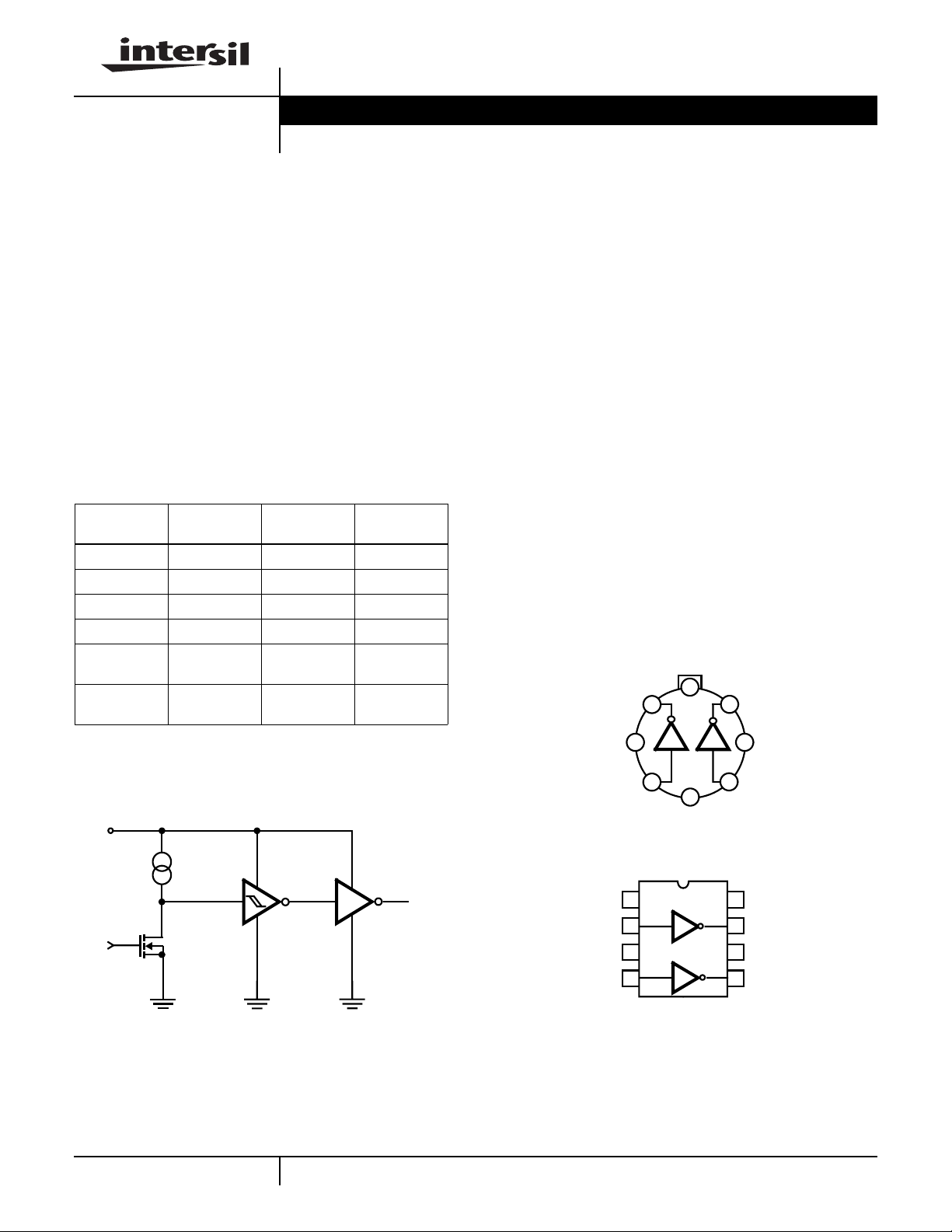
Functional Diagram
V
CC
≈2mA
File Number
Features
• Fast Rise and Fall Times
- 30ns with 1000pF Load
• Wide Supply Voltage Range
-V
= 4.5V to 15V
CC
• Low Power Consumption
- 4mW with Inputs Low
- 20mW with Inputs High
• TTL/CMOS Input Compatible Power Driver
-R
OUT
= 7Ω Typ
• Direct Interface with Common PWM Control ICs
• Pin Equivalent to DS0026/DS0056; TSC426
Applications
• Switching Power Supplies
• DC/DC Converters
• Motor Controllers
Pinouts
ICL7667 (CAN)
TOP VIEW
V+
8
IN A
1
2
3
TOP VIEW
OUT A
ICL7667 (PDIP, SOIC, CERDIP)
7
OUT B
6
N/CN/C
5
4
V-
IN B
2853.3
1
OUT
IN
3-73
CAUTION: These devices are sensitive to electrostatic discharge; follow proper IC Handling Procedures.
http://www.intersil.com or 407-727-9207
N/C
IN A
V-
IN B
2
3
4
| Copyright © Intersil Corporation 1999
8
7
6
5
N/C
OUT A
V+
OUT B

ICL7667
Absolute Maximum Ratings Thermal Information
Supply Voltage V+ to V-. . . . . . . . . . . . . . . . . . . . . . . . . . . . . . . .15V
Input Voltage . . . . . . . . . . . . . . . . . . . . . . . . . . V- -0.3V to V+ +0.3V
Package Dissipation, TA 25oC. . . . . . . . . . . . . . . . . . . . . . . .500mW
Operating Temperature Range
ICL7667C. . . . . . . . . . . . . . . . . . . . . . . . . . . . . . . . . . . . 0oC to 70oC
ICL7667M . . . . . . . . . . . . . . . . . . . . . . . . . . . . . . . . -55oC to 125oC
CAUTION: Stresses above those listed in “Absolute Maximum Ratings” may cause permanent damage to the device. This is a stress only rating and operationofthe
device at these or any other conditions above those indicated in the operational sections of this specification is not implied.
NOTE:
2. θJA is measured with the component mounted on an evaluation PC board in free air.
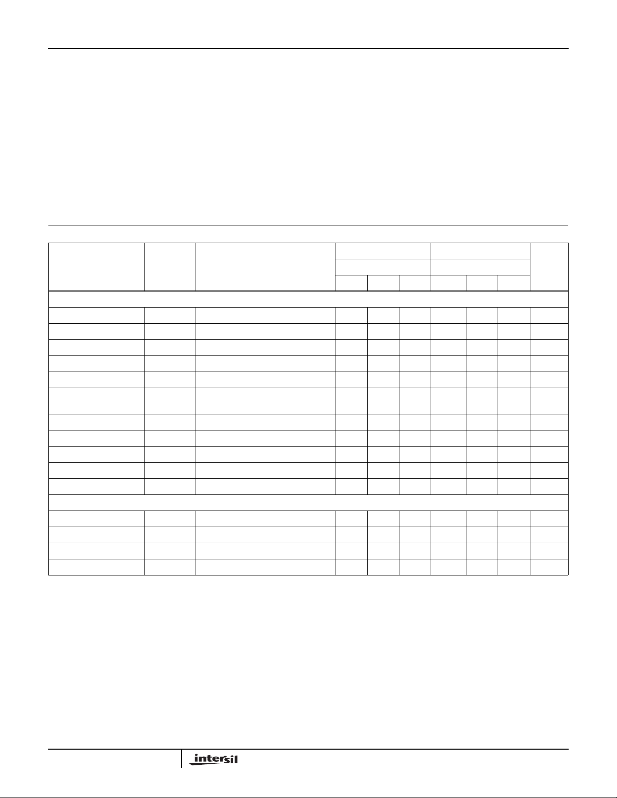
Electrical Specifications
PARAMETER SYMBOL TEST CONDITIONS
DC SPECIFICATIONS
Logic 1 Input Voltage V
Logic 1 Input Voltage V
Logic 0 Input Voltage V
Logic 0 Input Voltage V
Input Current I
Output Voltage High V
Output Voltage Low V
Output Resistance R
Output Resistance R
Power Supply Current I
Power Supply Current I
IL
OH
OL
OUT
OUT
CC
CC
SWITCHING SPECIFICATIONS
Delay Time T
D2
Rise Time T
Fall Time T
Delay Time T
D1
NOTE: All typical values have been characterized but are not tested.
VCC = 4.5V 2.0 - - 2.0 - - V
IH
VCC = 15V 2.0 - - 2.0 - - V
IH
VCC = 4.5V - - 0.8 - - 0.5 V
IL
VCC = 15V - - 0.8 - - 0.5 V
IL
VCC = 15V, VIN = 0V and 15V -0.1 - 0.1 -0.1 - 0.1 µA
VCC = 4.5V and 15V V
VCC = 4.5V and 15V - 0 0.05 - - 0.1 V
VIN = VIL, I
VIN = VIH, I
= -10mA, VCC = 15V - 7 10 - - 12 Ω
OUT
= 10mA, VCC = 15V - 8 12 - - 13 Ω
OUT
VCC = 15V, VIN = 3V both inputs - 5 7 - - 8 mA
VCC = 15V, VIN = 0V both inputs - 150 400 - - 400 µA
Figure 3 - 35 50 - - 60 ns
Figure 3 - 20 30 - - 40 ns
R
Figure 3 - 20 30 - - 40 ns
F
Figure 3 - 20 30 - - 40 ns
Thermal Resistance (Typical, Note 2) θJA(oC/W) θJC(oC/W)
PDIP Package . . . . . . . . . . . . . . . . . . . 150 N/A
SOIC Package . . . . . . . . . . . . . . . . . . . 170 N/A
Metal Can Package . . . . . . . . . . . . . . . 156 68
CERDIP Package. . . . . . . . . . . . . . . . . 115 30
Maximum Storage Temperature Range. . . . . . . . . . -65oC to 150oC
Maximum Lead Temperature (Soldering 10s) . . . . . . . . . . . . 300oC
(SOIC - Lead Tips Only)
ICL7667C, M ICL7667M
TA = 25oC -55oC ≤ TA≤ 125oC
MIN TYP MAX MIN TYP MAX
CC
-0.05
V
CC
-V
CC
-0.1
V
CC
UNITS
-V
3-74

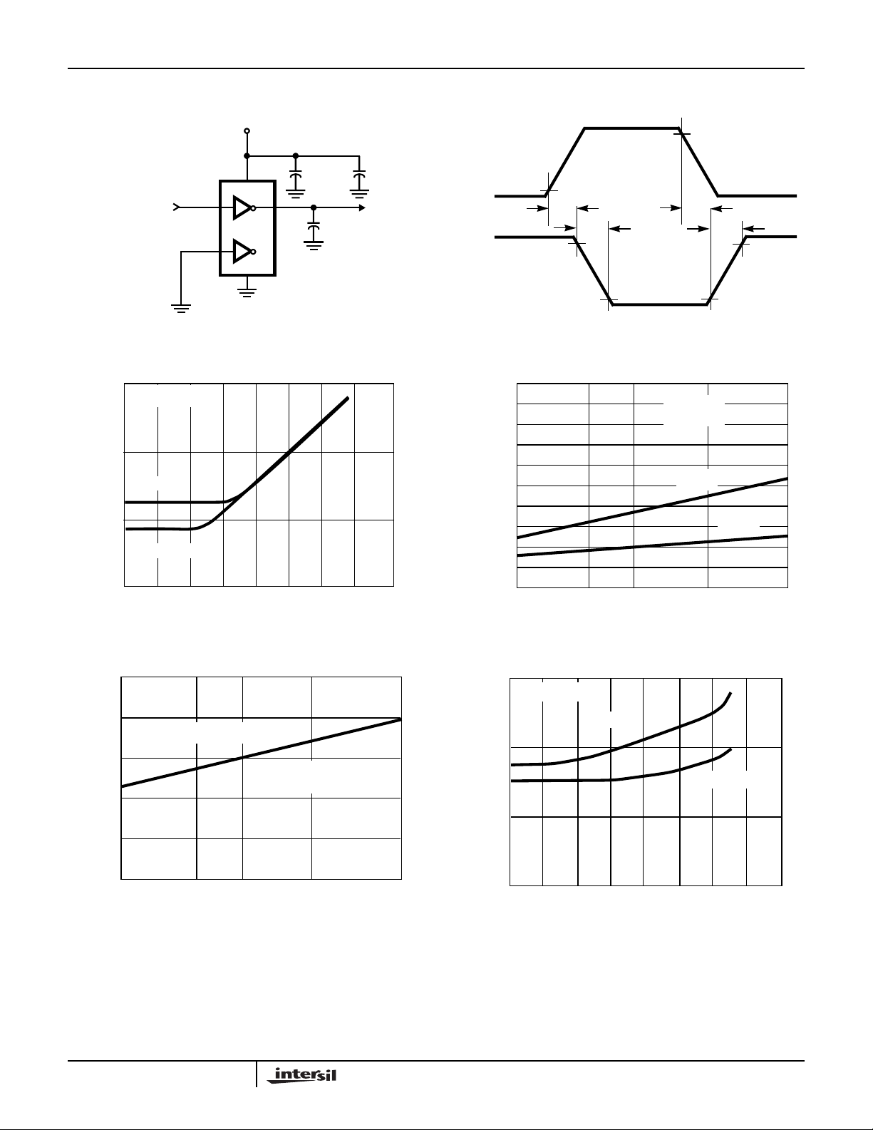
Test Circuits
ICL7667
V- = 15V
INPUT
ICL7667
INPUT RISE AND
FALL TIMES ≤ 10ns
Typical Performance Curves
1µs
100
, (ns)
f
AND t
r
t
10
VCC = 15V
t
RISE
t
FALL
1
10 100 1000 10K 100K
C
(pF)
L
+
4.7µF
0.1µF
CL = 1000pF
OUTPUT
INPUT
≈0.4V
OUTPUT
+5V
10%
T
D1
t
15V
0V
100
90
80
70
, (ns)
60
D2
50
AND T
40
D1
T
30
20
10
90%
0
-55 0 25 70 125
f
10%
TEMPERATURE (
90%
T
D2
CL = 1nF
VCC = 15V
T
D2
o
C)
t
r
10%
T
90%
D1
FIGURE 1. RISE AND FALL TIMES vs C
50
40
tr AND t
f
30
, (ns)
f
AND t
20
r
t
10
0
-55 0 25 70 125
TEMPERATURE (
CL = 1nF
= 15V
V
CC
o
C)
FIGURE 3. tr,tfvs TEMPERATURE FIGURE 4. ICC vs C
L
(mA)
CC
I
FIGURE 2. TD1, TD2 vs TEMPERATURE
30
VCC = 15V
200kHz
10
3.0
1
10 100 1K 10K
C
(pF)
L
20kHz
100K
L
3-75
 Loading...