Intersil Corporation ICL7665S Datasheet

ICL7665S
Data Sheet April 1999
CMOS Micropower Over/Under Voltage
Detector
The ICL7665S Super CMOS Micropower Over/Under
Voltage Detector contains two low power, individually
programmable Voltage detectors on a single CMOS chip.
Requiring typically 3µA for operation, the device is intended
for battery-operated systems and instruments which require
high or low voltage warnings, settable trip points, or fault
monitoring and correction. The trip points and hysteresis of
the two voltage detectors are individually programmed via
external resistors. An internal bandgap-type reference
provides an accurate threshold voltage while operating from
any supply in the 1.6V to 16V range.
The ICL7665S, Super Programmable Over/Under Voltage
Detector is a direct replacement for the industry standard
ICL7665B offering
ranges,
improved
temperature coefficient, and
current. All improvements are highlighted in the electrical
characteristics section.
guaranteed over the entire commercial and industrial
temperature ranges.
wider
operating voltage and temperature
threshold accuracy (ICL7665SA), and
guaranteed
maximum supply
All critical parameters are
File Number
3182.4
Features
• Guaranteed 10µA Maximum Quiescent Current Over
Temperature
• Guaranteed Wider Operating Voltage Range Over Entire
Operating Temperature Range
• 2% Threshold Accuracy (ICL7665SA)
• Dual Comparator with Precision Internal Reference
• 100ppm/oC Temperature Coefficient of Threshold Voltage
• 100% Tested at 2V
• Output Current Sinking Ability . . . . . . . . . . . . Up to 20mA
• Individually ProgrammableUpper and Lower Trip Voltages
and Hysteresis Levels
Applications
• Pocket Pagers
• Portable Instrumentation
• Charging Systems
• Memory Power Back-Up
Ordering Information
TEMP. RANGE
PART NUMBER
ICL7665SCBA 0 to 70 8 Ld SOIC (N) M8.15
ICL7665SCPA 0 to 70 8 Ld PDIP E8.3
ICL7665SACBA 0 to 70 8 Ld SOIC (N) M8.15
ICL7665SACPA 0 to 70 8 Ld PDIP E8.3
ICL7665SIBA -40 to 85 8 Ld SOIC (N) M8.15
ICL7665SIPA -40 to 85 8 Ld PDIP E8.3
ICL7665SAIBA -40 to 85 8 Ld SOIC (N) M8.15
ICL7665SAIPA -40 to 85 8 Ld PDIP E8.3
(oC) PACKAGE PKG. NO.
• Battery Operated Systems
• Portable Computers
• Level Detectors
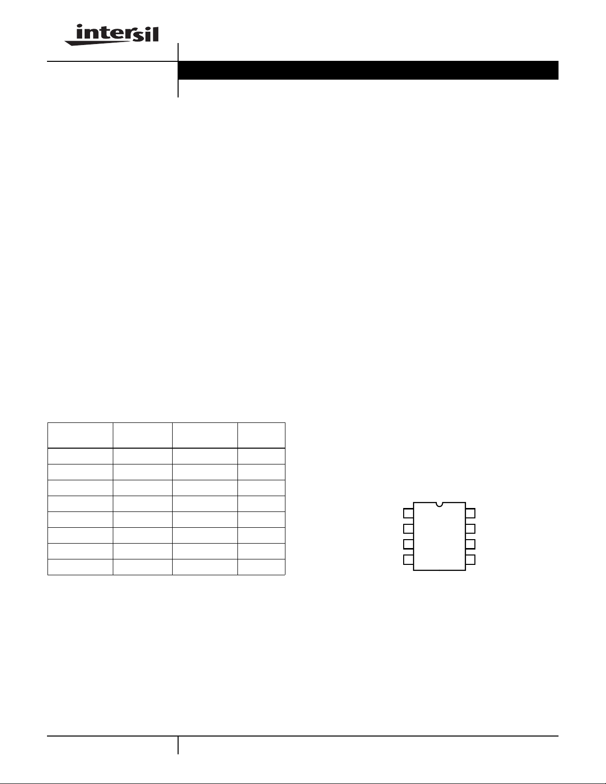
Pinout
ICL7665S
(SOIC, PDIP)
TOP VIEW
1
OUT 1
SET 1
GND
2
3
4
HYST 1
8
7
6
5
V+
OUT 2
SET 2
HYST 2
3-62
CAUTION: These devices are sensitive to electrostatic discharge; follow proper IC Handling Procedures.
http://www.intersil.com or 407-727-9207
| Copyright © Intersil Corporation 1999

ICL7665S
Absolute Maximum Ratings Thermal Information
Supply Voltage (Note 2). . . . . . . . . . . . . . . . . . . . . . . . . -0.3 to +18V
Output Voltages OUT1 and OUT2. . . . . . . . . . . . . . . . .-0.3V to 18V
(with respect to GND) (Note 2)
Output Voltages HYST1 and HYST2. . . . . . . . . . . . . .-0.3V to +18V
(with respect to V+) (Note 2)
Input Voltages SET1 and SET2. . . . . (GND -0.3V) to (V+ V- +0.3V)
(Note 2)
Maximum Sink Output OUT1 and OUT2 . . . . . . . . . . . . . . . . . 25mA
Maximum Source Output Current
HYST1 and HYST2 . . . . . . . . . . . . . . . . . . . . . . . . . . . . . . -25mA
Operating Conditions
Temperature Range
ICL7665SC. . . . . . . . . . . . . . . . . . . . . . . . . . . . . . . . . 0oC to 70oC
ICL7665SI . . . . . . . . . . . . . . . . . . . . . . . . . . . . . . . -40oC to 85oC
CAUTION: Stresses above those listed in “Absolute Maximum Ratings” may cause permanent damage to the device. This is a stress only rating and operationofthe
device at these or any other conditions above those indicated in the operational sections of this specification is not implied.
NOTES:
1. θJA is measured with the component mounted on an evaluation PC board in free air.
2. Due to the SCR structure inherent in the CMOS process used to fabricate these devices, connecting any terminal to voltages greater than (V+
+0.3V) or less than (GND - 0.3V) may cause destructive device latchup. For these reasons, it is recommended that no inputs from external
sources not operating from the same power supply be applied to the device before its supply is established, and that in multiple supply systems,
the supply to the ICL7665S be turned on first. If this is not possible, current into inputs and/or outputs must be limited to ±0.5mA and voltages
must not exceed those defined above.
Thermal Resistance (Typical, Note 1) θJA (oC/W) θJC (oC/W)
PDIP Package . . . . . . . . . . . . . . . . . . . 150 N/A
Plastic SOIC Package . . . . . . . . . . . . . 180 N/A
Maximum Junction Temperature (Plastic) . . . . . . . . . . . . . . . .150oC
Maximum Junction Temperature (CERDIP). . . . . . . . . . . . . . .175oC
Maximum Storage Temperature Range. . . . . . . . . . -65oC to 150oC
Maximum Lead Temperature (Soldering 10s) . . . . . . . . . . . . .300oC
(SOIC - Lead Tips Only)
Electrical Specifications The specifications below are applicable to both the ICL7665S and ICL7665SA. V+ = 5V, T
Test Circuit Figure 7. Unless Otherwise Specified
PARAMETER SYMBOL TEST CONDITIONS MIN TYP MAX UNITS
Operating Supply Voltage V+ ICL7665S T
ICL7665SA 0oC ≤ TA≤ 70oC 1.8 - 16 V
Supply Current I+ GND ≤ V
SET1
, V
SET2
0oC ≤ TA≤ 70oC V+ = 2V - 2.5 10 µA
-40oC ≤ TA≤ 85oC V+ = 2V - 2.5 10 µA
Input Trip Voltage V
Temperature Coefficient of
V
SET
Supply Voltage Sensitivity of
V
, V
SET1
SET2
V
V
V
∆V
∆V
SET1
SET2
SET1
SET2
SET
∆T
SET
∆V
ICL7665S 1.20 1.30 1.40 V
ICL7665SA 1.275 1.30 1.325 V
ICL7665S - 200 - ppm
ICL7665SA - 100 - ppm
R
, R
OUT2
, R
HYST1
S
OUT1
2V ≤ V+ ≤ 10V
= 25oC 1.6 - 16 V
A
0oC ≤ TA≤ 70oC 1.8 - 16 V
-25oC ≤ TA≤ 85oC 1.8 - 16 V
-25oC ≤ TA≤ 85oC 1.8 - 16 V
≤ V+, All Outputs Open Circuit
V+ = 9V - 2.6 10 µA
V+ = 15V - 2.9 10 µA
V+ = 9V - 2.6 10 µA
V+ = 15V - 2.9 10 µA
1.20 1.30 1.40 V
1.275 1.30 1.325 V
, R
2HYST2
= 1MΩ,
- 0.03 - %/V
= 25oC,
A
3-63

ICL7665S
Electrical Specifications The specifications below are applicable to both the ICL7665S and ICL7665SA. V+ = 5V, T
Test Circuit Figure 7. Unless Otherwise Specified (Continued)
PARAMETER SYMBOL TEST CONDITIONS MIN TYP MAX UNITS
Output Leakage Currents of
OUT and HYST
Output Saturation Voltages V
Output Saturation Voltages V
Output Saturation Voltages V
Output Saturation Voltages V
V
Input Leakage Current I
SET
∆ Input for Complete Output
Change
Difference in Trip Voltages V
Output/Hysteresis
Difference
NOTES:
3. Derate above 25oC ambient temperature at 4mW/oC
4. All significant improvements over the industry standard ICL7665 are highlighted.
I
OLK
I
HLK
I
OLK
I
HLK
OUT1
HYST1VSET1
OUT2
HYST2VSET2
SET
∆V
SET
SET1
V
SET2
V
SET
V+ = 15V, TA = 70oC - - 2000 nA
V
SET1
I
OUT1
I
HYST1
V
SET2
I
OUT2
GND ≤ V
R
OUT
R
HYST
V
OUT
V
OUT
-
R
OUT
R
OUT
= 0V or V
≥ 2V - 10 200 nA
SET
- -10 -100 nA
- - -500 nA
= 2V,
= 2mA
V+ = 2V - 0.2 0.5 V
V+ = 5V - 0.1 0.3 V
V+ = 15V - 0.06 0.2 V
= 2V,
= -0.5mA
V+ = 2V - -0.15 -0.30 V
V+ = 5V - -0.05 -0.15 V
V+ = 15V - -0.02 -0.10 V
= 0V,
= 2mA
V+ = 2V - 0.2 0.5 V
V+ = 5V - 0.15 0.3 V
V+ = 15V - 0.11 0.25 V
= 2V V+ = 2V, I
V+ = 5V, I
V+ = 15V, I
≤ V+ - 0.01 10 nA
SET
= 4.7kΩ,
= 20kΩ,
LO = 1% V+,
ICL7665S - 1.0 - mV
ICL7665SA - 0.1 - mV
= -0.2mA - -0.25 -0.8 V
HYST2
= -0.5mA - -0.43 -1.0 V
HYST2
= -0.5mA - -0.35 -0.8 V
HYST2
HI = 99% V+
, R
= 1mW - ±5 ±50 mV
HYST
, R
= 1mW ICL7665S - ±1-mV
HYST
ICL7665SA - ±0.1 - mV
= 25oC,
A
AC Electrical Specifications
PARAMETER SYMBOL TEST CONDITIONS MIN TYP MAX UNITS
OUTPUT DELAY TIMES
Input Going HI t
Input Going LO t
3-64
SO1D
t
SH1D
t
SO2D
t
SH2D
SO1D
t
SH1D
t
SO2D
t
SH2D
V
Switched between 1.0V to 1.6V
SET
R
= 4.7kΩ, CL = 12pF
OUT
R
= 20kΩ, CL = 12pF
HYST
V
Switched between 1.6V to 1.0V
SET
R
= 4.7kΩ, CL = 12pF
OUT
R
= 20kΩ, CL = 12pF
HYST
-85-µs
-90-µs
-55-µs
-55-µs
-75-µs
-80-µs
-60-µs
-60-µs

ICL7665S
AC Electrical Specifications (Continued)
PARAMETER SYMBOL TEST CONDITIONS MIN TYP MAX UNITS
Output Rise Times t
Output Fall Times t
O1R
t
O2R
t
H1R
t
H2R
O1F
t
O2F
t
H1F
t
H2F
V
Switched between 1.0V to 1.6V
SET
R
= 4.7kΩ, CL = 12pF
OUT
R
= 20kΩ, CL = 12pF
HYST
V
Switched between 1.0V to 1.6V
SET
R
= 4.7kΩ, CL = 12pF
OUT
R
= 20kΩ, CL = 12pF
HYST
- 0.6 - µs
- 0.8 - µs
- 7.5 - µs
- 0.7 - µs
- 0.6 - µs
- 0.7 - µs
- 4.0 - µs
- 1.8 - µs
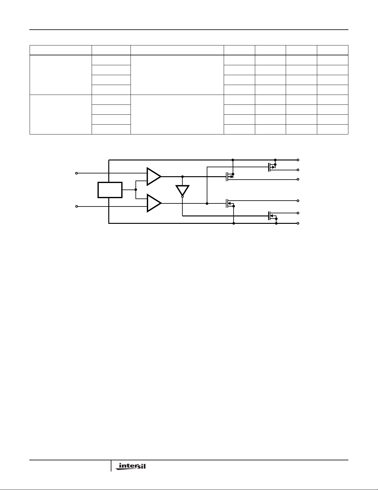
Functional Block Diagram
V+
SET1
+
REF
HYST2
HYST1
SET2
CONDITIONS (Note 5)
V
> 1.3V, OUT1 Switch ON, HYST1 Switch ON
SET1
V
< 1.3V, OUT1 Switch OFF, HYST1 Switch OFF
SET1
V
> 1.3V, OUT2 Switch OFF, HYST2 Switch ON
SET2
V
< 1.3V, OUT2 Switch ON, HYST2 Switch OFF
SET2
NOTE:
5. See Electrical Specifications for exact thresholds.
+
-
OUT2
OUT1
GND
3-65
 Loading...