Intersil Corporation ICL7663SACBA, ICL7663SACPA, ICL7663SAIPA, ICL7663SCPA Datasheet

TM
ICL7663S
Data Sheet April 1999
CMOS Programmable Micropower
Positive Voltage Regulator
The ICL7663S Super Programmable Micropower Voltage
Regulator is a low power, high efficiency positive voltage
regulator which accepts 1.6V to 16V inputs and provides
adjustable outputs from 1.3V to 16V at currents up to 40mA.
It is a direct replacem ent for the industry stan dard ICL7663B
offering wider operating voltage and temper ature ranges,
improved output acc uracy ( ICL7663SA) , better t empera ture
coefficient, guaranteed maximum supply current, and
guaranteed line and load regulation. All improvements are
highlighted in the electrical characteristics section. Critical
parameters ar e guaranteed over the entire commercial
and industrial temperature ranges. The ICL7663S/SA
programmable out put voltage is set by two ext ernal resist ors.
The 1% referen ce a ccuracy of the I CL766 3SA eli minates the
need for trimming the output voltage in most applications.
The ICL7663S is well suit ed for battery powered supplies,
featuring 4µA quiesce nt current , low V
output curren t sensing and logic input level shutdown
control. In addi tion, the ICL7663S has a negative
temperature coefficient output sui table for generating a
temperature compensated display drive voltage for LCD
displays.
IN
to V
differential ,
OUT
File Number 3180.3
Features
• Guaranteed 10µA Maximum Quiescent Current Over All
Temperature Ranges
• Wider Operati ng Voltage Range - 1.6V to 16V
• Guaranteed Line and Load Regulation Over Entire
Operating Temperat ure Range Optional
• 1% Output Voltage Accuracy (ICL7663SA)
• Output Voltage Programmable from 1.3V to 16V
• Improved Temperature Coefficient of Output Voltage
• 40mA Minimum Output Current with Current Limiting
• Output Voltages with Programmable Negative
Temperature Coefficients
• Output Shutdown via Current-Limit Sensing or External
Logic Level
• Low Input-to-Output Voltage Differential
• Improved Direct Replacement for Industry Standard
ICL7663B and Other Second-Source Products
Applications
• Low-Power Portable Inst rumentation
• Pagers
Ordering Information
TEMP. RANGE
PART NUMBER
ICL7663SCBA 0
ICL7663SCPA 0 to 70 8 Ld PDIP E8.3
ICL7663SACBA 0
ICL7663SACPA 0
ICL7663SIBA -25 to 85 8 Ld SOIC (N) M8.15
ICL7663SIPA -25
ICL7663SAIBA -25
ICL7663SAIPA -25 to 85 8 Ld PDIP E8.3
(oC) PACKAGE PKG. NO.
to 70 8 Ld SOIC (N) M8.15
to 70 8 Ld SOIC (N) M8.15
to 70 8 Ld PDIP E8.3
to 85 8 Ld PDIP E8.3
to 85 8 Ld SOIC (N) M8.15
• Handheld Inst ruments
• LCD Display Modules
• Remote Data Loggers
• Battery-Powered Systems
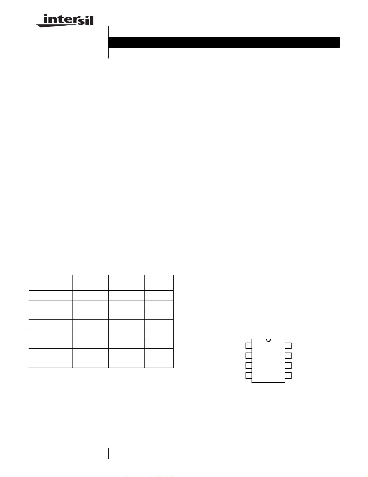
Pinout
ICL7663S
(PDIP, CERDIP, SOIC)
TOP VIEW
V
V
OUT2
OUT1
GND
1
2
3
4
SENSE
8
7
6
5
VIN+
V
TC
V
SET
SHDN
55
CAUTION: These devices are sensitive to electrostatic discharge; follow proper IC Handling Procedures.
1-888-INTERSIL or 321-724-7143
| Intersil (and design) is a trademark of Intersil Americas Inc.
Copyright © Intersil Americas Inc. 2001. All Rights Reserved

ICL7663S
Absolute Maximum Ratings Thermal Information
Input Supply Voltage . . . . . . . . . . . . . . . . . . . . . . . . . . . . . . . . .+18V
Any Input or Output Voltage (Note 1 )
Terminal s 1, 2, 3, 5, 6, 7. . . . . . . . . . . . . V
+ 0.3V to GND -0.3V
IN
Output Source Current
Terminal 2 . . . . . . . . . . . . . . . . . . . . . . . . . . . . . . . . . . . . . . 50mA
Terminal 3 . . . . . . . . . . . . . . . . . . . . . . . . . . . . . . . . . . . . . . 25mA
Output Sinking Current
Terminal 7 . . . . . . . . . . . . . . . . . . . . . . . . . . . . . . . . . . . . . -10mA
Operating C o ndi t io ns
Temperature R an ge
ICL7663SC. . . . . . . . . . . . . . . . . . . . . . . . . . . . . . . . . 0
ICL7663SI . . . . . . . . . . . . . . . . . . . . . . . . . . . . . . . -25
CAUTION: Stress es abov e thos e lis ted in “ A bsolute Max imum R a tings” ma y cause per manen t dam age to th e de vice. This is a s tress on ly rating and ope rat ion of th e
device at these or any other conditions above those indicated in the operational sections of this specification is not implied.
NOTES:
1. Connecting any terminal to voltages greater than (V+
mended that no inputs from s ources ope rating on external power supplies be applied prior to ICL7663S power-up.
is measured with the componen t mounted on an evaluation PC board in free air.
2. θ
JA
o
C to 70oC
o
C to 85oC
+ 0.3V) or less than (GND - 0.3V) may cause destructive device latch-up. It is recom-
IN
Thermal Resistance (Typical, Note 2) θ
(oC/W) θJC (oC/W)
JA
CERDIP Package. . . . . . . . . . . . . . . . . 115 30
PDIP Package . . . . . . . . . . . . . . . . . . . 150 N/A
Plastic SOIC Package . . . . . . . . . . . . . 180 N/A
Maximum Junction Temperature
PDIP Package . . . . . . . . . . . . . . . . . . . . . . . . . . . . . . . . . 150
CERDIP Package. . . . . . . . . . . . . . . . . . . . . . . . . . . . . . . 175
Maximum Storage Temperature Range . . . . . . . . . -65
o
C to 150oC
Maximum Lead Temperature (Soldering 10s) . . . . . . . . . . . . .300
(SOIC - Lead Tips On ly)
o
C
o
C
o
C
Electrical Specifications Specifications B elow Applicable to Both ICL7663S and IC L7663SA, Unless Otherwi se Specified. V+
V
= 5V, TA = 25oC, Unless Otherwise Specified. Notes 4, 5. See Test Circ uit, Figure 7
OUT
PARAMETER SYMBOL TEST CONDITIONS MIN TYP MAX UNITS
Input Voltage V+
Quie sc en t C urr e nt I
Refere nce Volta ge V
Temperature
∆V
Coefficient
Line Regulation ∆V
V
SET’
V
Input Current I
SET
Shutdown Input Current I
Shutdown Input Voltage V
Sense Pin Input Current I
SHDN
SHDN
SENSE
Sense Pin Input Threshold V
SET
∆T
SET
ICL7663S TA = 25oC1.5-16V
IN
o
0
C < TA < 70oC1.6-16V
-25oC < TA < 85oC1.6- 16V
ICL7663SA 0
1.4V ≤ V
Q
V+
≤ 8.5V, No Load
OUT
= 9V 0oC < TA < 70oC--10µA
IN
o
C < TA < 70oC1.6-16V
o
-25
C < TA < 85oC1.6- 16V
o
-25
C < TA < 85oC--10µA
V+IN = 16V 0oC < TA < 70oC--12µA
o
-25
C < TA < 85oC--12µA
I
OUT1
= 100µA, V
OUT
= V
SET
ICL7663S TA = 25oC 1.2 1.3 1.4 V
SET
ICL7663SA T
o
0
C < TA < 70oC - 100 - ppm
= 25oC 1.275 1.29 1.305 V
A
-25oC < TA < 85oC - 100 - ppm
2V < VIN < 15V 0oC < TA < 70oC-0.03-%/V
SET
∆V
IN
o
-25
C < TA < 85oC - 0.03 0.3 %/V
0oC < TA < 70oC - 0.01 10 nA
o
-25
C < TA < 85oC - 0.01 10 nA
- ±0.01 10 nA
V
SHDN
V
SHDN
HI: Both V
LO: Both V
Disabled 1.4 - - V
OUT
Enable - - 0.3 V
OUT
-0.0110nA
CL
-0.5- V
= 9V,
IN
56

ICL7663S
Electrical Specifications Specifications B elow Applicable to Both ICL7663S and IC L7663SA, Unless Otherwi se Specified. V+
V
= 5V, TA = 25oC, Unless Otherwise Specified. Notes 4, 5. See Test Circ uit, Figure 7 (Continued)
OUT
= 9V,
IN
PARAMETER SYMBOL TEST CONDITIONS MIN TYP MAX UNITS
Input-Outp ut Sat ura ti on
Resistance (Note 3)
Load Regulation ∆V
Available Output Current
(V
)
OUT2
Negative Tempco Output
(Note 4)
Temperature Coeff icient ∆V
R
SAT
OUT
∆I
OUT
I
OUT2
V
TC
I
TC
V+IN = 2V, I
V+IN = 9V, I
V+
= 15V, I
IN
1mA < I
OUT2
50µA < I
OUT1
3V ≤ VIN ≤ 16V, VIN - V
= 1mA - 170 350 Ω
OUT1
= 2mA - 50 100 Ω
OUT1
= 5mA - 35 70 Ω
OUT1
< 20mA - 1 3 Ω
< 5mA - 2 10 Ω
= 1.5V 40 - - mA
OUT2
Open Circ ui t Volt age - 0.9 - V
Maximum Sink Current 0 8 2.0 mA
Open Circuit - +2.5 - mV/
TC
∆T
Minimum Load Current I
L(MIN)
Includes V
Divider TA = 25oC--1.0µA
SET
0oC < TA < 70oC-0.25.0µA
o
-25
C < TA < 85oC-0.25.0µA
NOTES:
3. This parameter refers to the saturation resistance of the MOS pass transistor. The minimum input-output voltage differential at low curre nt (u nder
5mA), can be determined by multiplying the load current (including set resist or curren t, but not quiescent current) by this resistance.
4. This output has a positive temperature coefficient. Using it in combination with the inverting input of the regul ator at V
coefficient results in the output voltage. See Figure 9 for details. Pin will not source current.
, a negative
SET
5. All pins are designed to withstand electrostatic discharge (ESD) levels in excess of 2000V.
6. All significant improvements over the industry standard IC L7663 are highlighted.
o
C
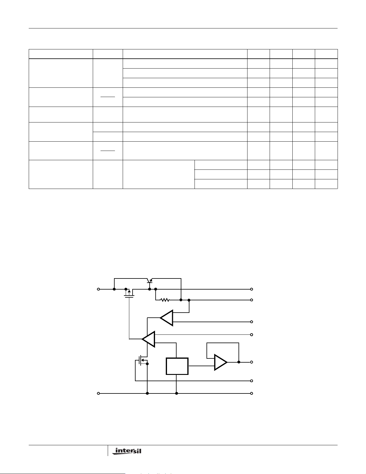
Functional Diagram
V+
GND
8
IN
C
A
REF
B
3
V
2
V
1
SENSE
6
V
7
V
5
SHUTDOWN
4
GND
OUT1
OUT2
SET
TC
57
 Loading...